ORGANIC ELECTRONICS PROCESS DEVELOPMENT AND ENCAPSULATION TECHNOLOGIES
|
|
|
- Helena Wright
- 6 years ago
- Views:
Transcription

1 FRAUNHOFER INSTITUTE FOR ORGANIC ELECTRONICS, ELECTRON BEAM AND PLASMA TECHNOLOGY FEP ORGANIC ELECTRONICS PROCESS DEVELOPMENT AND ENCAPSULATION TECHNOLOGIES
2 2


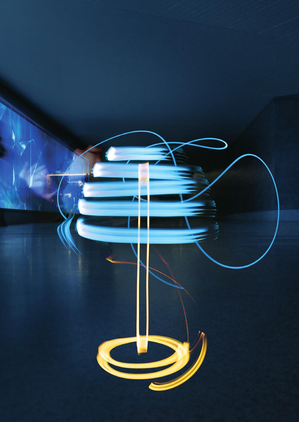
3 PROFILE Fraunhofer FEP combines research and development works for the production, integration and technology of organic electronic devices. The focus is on diverse applications entering industrial production as well as consumer goods applications based on semiconducting organic materials e.g. in lighting, information, automotive, medical and environmental technologies, as well as safety technology; really almost every sphere of life. SERVICES AT A GLANCE Feasibility and market studies Simulations Processes for flexible OLED lighting at various substrates, bi-directional OLED microdisplays and ultra-high barrier films for encapsulation are under development. Fraunhofer FEP can be partner for customer- and application orientated research, development and pilot fabrication of novel module concepts and fabrication methods for these organic electronic devices. Complete process development Device & system development Prototypes & demonstrators The institute provides full service from system design and technological development to pilot production of small batches including substrate structuring, deposition technology, encapsulation and system integration. Characterization & test Pilot fabrication Trainings Consulting services Dresden street artist and up-and-coming product designer Frank Hahnewald produced the mesmerizing light illustrations on the left page by photographing colored Fraunhofer FEP OLED modules while moving them in complete darkness. Using long exposure times he created complex, dynamic trails of light. 3
4 4

5 FLEXIBLE ORGANIC ELECTRONICS TECHNOLOGY Process development of OLED and organic solar cells Vacuum thermal evaporation (VTE) Litho-free substrate patterning Sputtering Material evaluation, stack integration Encapsulation Characterization Roll-to-roll technology for SM-OLED System design COMPONENTS Monochrome and white OLED modules Large area lighting panels Transparent OLED modules Customized layouts Flexible OLED on polymer web, metal strips, thin flexible glass APPLICATIONS General lighting, automotive lighting, professional lighting Signage Display Sensorics MATERIAL EVALUATION Transparent conducting oxides (TCO) Silber nanowires (AgNW) Graphene Carbon nanotubes (CNT) Benchmarking of active materials Synthetic metals, conductive polymers, metals Hole transport / electron transport materials Singlett / triplett emitter Light absorber for OPD / OPV Passive materials: thin-glass, metalband, silicon wafer Barrier films, glues, desiccants Climatic chamber with or without sun simulator Substrates rigid / flexible, e.g. polymer films, paper, glass, 5

 Organic photodiodes (OPD) All modules available on flexible or on rigid substrates All OLED-modules available transparent or opaque")
6 SHEET-TO-SHEET PROCESS TECHNOLOGY TECHNOLOGY Vacuum thermal evaporation (VTE) Organic vapor phase deposition Atomic layer deposition (ALD) Slot die coating Spin coating ITO sputtering Gravure printing Lamination of barrier films Laser ablation / laser patterning Thin film encapsulation Foil and glass encapsulation Scribe and break Foil lamination (ambient or inert) Automated optical inspection Customized wet cleaning Etching Screen printing (metal and passivation layer) APPLICATIONS OLED lighting Organic photovoltaic (OPV) Organic photodiodes (OPD) All modules available on flexible or on rigid substrates All OLED-modules available transparent or opaque Color-tunable modules 6


7 ROLL-TO-ROLL PROCESS TECHNOLOGY TECHNOLOGY Vacuum thermal evaporation (VTE) OLED small-molecule evaporation Plasma pre-treatments Web cleaning Lamination of barrier films Organic electronic devices on metal and plastic web Sputtering process of metal and metal oxide layers Gravure printing and slot die coating APPLICATIONS OLED lighting Organic photovoltaic Organic photodiodes All modules available on flexible or on rigid substrates All OLED-modules available transparent or opaque Color-tunable modules 7
8 8
 Encapsulation including wafer-level color filter integration Pilot line OLED / PLED-on-silicon (8 Si wafer) COMPONENTS OLED microdisplays (QVGA, VGA, XGA,.")

9 OLED photodetectors Si CMOS chip carrier PCB MICRODISPLAYS AND SENSORS TECHNOLOGY Process development of small-molecules (OLED) and polymers (PLED) Silicon-CMOS / OLED interface definition (with silicon foundry) Encapsulation including wafer-level color filter integration Pilot line OLED / PLED-on-silicon (8 Si wafer) COMPONENTS OLED microdisplays (QVGA, VGA, XGA,...) System design (electronics, optics) Device characterization Bidirectional OLED microdisplays (with embedded image sensor) OLED as silicon-embedded patterned light source and CMOS photodetectors Silicon-CMOS backplane IC design (CMOS processes ( µm) APPLICATIONS See-through head-mounted displays (ST-HMD) Electronic view-finder (EVF) Optical inspection Autostereoscopic 3D displays Interactive ST-HMD (embedded eye-tracking / gaze-control) Optical sensors (fluorescence, flowmetry, color,...) 9

 Optical inspection via microscope APPLICATIONS OLED microdisplays Organic photodiodes (OPD) Organic devices for sensor applications Flexible organic devices")
10 ORGANIC MICROELECTRONIC DEVICES TECHNOLOGY Technology on 200 mm wafer Orthogonal photolithography Electron beam evaporation Sputter processes Barix TM encapsulation 1:1 lithography process to structure organic and inorganic layer Thermal evaporation of organic materials Structuring of layers via etching, lift-off or shadow masks Shadow mask fine alignment with ± 10 µm alignment accuracy Fully automated wafer bonding Wafer prober for electro-optical characterization Ellipsometer for thin-film characterization Lamination of foil onto wafer for flexible devices Various substrates possible (glass, silicon wafer, foil) Optical inspection via microscope APPLICATIONS OLED microdisplays Organic photodiodes (OPD) Organic devices for sensor applications Flexible organic devices Inorganic color filters 10


11 OLED illumination module Size comparison Reaction chamber for algae IC AND SYSTEM DESIGN TECHNOLOGY Development of integrated circuits Analog, digital, mixed-signal Software design C, C++, VHDL Typical CMOS processes: 0.13 µm / 0.18 µm / 0.35 µm Concept, system design, schematic, simulation, layout, verification Coordination with external silicon wafer manufacturer, test and start-up Development of discrete electronics Based on commercial ICs, FPGA, microcontroller etc. Concept, system design, schematic, PCB layout Coordination with external manufacturer, test and start-up Microcontroller firmware, embedded systems, application software COMPONENTS Microdisplay and sensor backplane Driving and readout electronics for microdisplays, sensors, OLED and OPD Device driver, software libraries and applications APPLICATIONS Head mounted displays Sensors Lab on chip Image processing, focus on eye-tracking 11
12 12
 Near field goniometer measurements (angular dependent absolute spectral radiance and related parameters, e.")
13 CHARACTERIZATION AND ANALYTICS PHOTOMETRIC CHARACTERIZATION 1 m-integrating sphere measurements (absolute spectral radiant flux and related parameters, e.g. luminous efficacy and color coordinates) Near field goniometer measurements (angular dependent absolute spectral radiance and related parameters, e.g. luminance and color coordinates) Calibrated CCD camera measurements (spacial luminance distribution) SPECTROSCOPIC THIN FILM CHARACTERIZATION Transmission and reflection spectroscopy in UV-VIS-NIR range Variable angle spectroscopic ellipsometry Photoluminescence spectroscopy Thin-film modelling for analysis of spectroscopic data SOLAR CELL CHARACTERIZATION Solar cell test system (IV-characteristics with sun simulator) Photocurrent mapper GENERAL DEVICE CHARACTERIZATION Lifetime and reliability testing of OLED modules Climatic chamber testing IR imaging for thermal characterization and failure analysis 13
14 14

![Our technologies include: Technology Productivity (line speed) m/min WVTR at 38 C / 90% r.h. [g/(m² d)] Hollow-cathode plasma-assisted evaporation (HAD) 600 1 Reactive sputtering of oxides 1 0.](/docs-images/79/79683613/images/15-1.jpg "005 Multi-layer stack: sputtering + wet coating of ORMOCER * 1 0.0002 Multi-layer stack single pass. sputtering + arcpecvd 4 0.005 Atomic layer deposition Static process < 0.")
15 PERMEATION BARRIERS The department Flexible Products pursues various technological approaches to manufacture high quality and cost-efficient water vapor and oxygen barrier coatings on flexible substrates. For each application, we can provide the best suitable technological approach taking into account technical requirements and economic targets. Our technologies include: Technology Productivity (line speed) m/min WVTR at 38 C / 90% r.h. [g/(m² d)] Hollow-cathode plasma-assisted evaporation (HAD) Reactive sputtering of oxides Multi-layer stack: sputtering + wet coating of ORMOCER * Multi-layer stack single pass. sputtering + arcpecvd Atomic layer deposition Static process < * Cooperation within Fraunhofer Polymer Surfaces Alliance POLO OUR OFFER Our services and products around permeation barrier coatings, their application and related products include, but not limited to: Evaluation of polymer substrates for barriers Sampling, material provision and feasibility studies Roll-to-roll pilot production of barrier film rolls Adaption of barrier films to specific application Functional film design and deposition (including electrodes, adapted optics or protection layers) Product integration Technology transfer and licensing Key components for barrier layer deposition Direct thin-film encapsulation of devices Barrier film and device characterization 15
 Calcium-mirror test for WVTR and defect characterization OLED degradation and lifetime studies")

16 FILM AND DEVICE CHARACTERIZATION In our Flexible Organic Electronics Lab we are able to test permeation barriers directly on a device. Our analytical portfolio comprises: Coulometric permeation measurement (BRUGGER WDDG, Mocon OX-TRAN) Calcium-mirror test for WVTR and defect characterization OLED degradation and lifetime studies (Roll-to-roll) particle and defect inspection Mechanical bending and strain tests APPLICATIONS Beside our lead applications, flexible smart packaging and flexible organic electronics, our technologies can be easily adapted to: Flexible and organic photovoltaic devices Electrochromic systems Thin film energy harvesting and energy storage devices Holographic systems on polymers Sensors and flexible / organic transistors Quantum dot and OLED lighting and displays Wearables and other flexible electronic devices 16


17 EQUIPMENT labflex mm web width sputtering and PECVD Roll-to-roll OLED encapsulation without roller contact of coated side coflex 600 and novoflex mm web with (pilot scale) sputtering, PECVD and evaporation multilayer deposition in one run web speed up to 10 m/s double-side coating Production line OLED on Silicon Etching / sputtering Spin coating Nitrogen oven Deposition by thermal evaporation and Barix thinfilm encapsulation Full-automated wafer bonding system Wafer prober Microscopes Ellipsometer Roll-to-roll OLED line Deposition by thermal linear evaporation Reactive sputter magnetron and plasma pre-treatment Rewinding unit with integrated optical inspection system Coating and printing unit under inert atmosphere Barrier film encapsulation under inert atmosphere 300 mm width; metal, polymer, thin glass Pilot line for organic devices on sheet level (rigid or flexible) Vaccum thermal evaporation systems Organic vapor phase deposition system Slot die coater Atomic layer deposition tool Magnetron sputter source Automated screen and stencil printer Laserablation system Wet cleaning tools Glass scribe and break tool Foil lamination systems (ambient or inert) Automated optical inspection Rigid and flexible substrates up to mm² (several processes up to mm²) 17
 Cost-efficient manufacturing techniques High brightness, high resolution microdisplays Extended temperature range (sensors) Extended spectral emission/detection (UV, IR,.")

18 OUTLOOK OLED ON SILICON Smart microdisplays (e.g., embedded eye-tracking) Cost-efficient manufacturing techniques High brightness, high resolution microdisplays Extended temperature range (sensors) Extended spectral emission/detection (UV, IR,...) Inorganic colour filter Organic photodiodes in UV / VIS / NIR Lithography structuring of organic layer Bendable devices R,G,B-micropatterning full color / without color filter Applications e.g. food quality, point-of-use diagnostics,... FLEXIBLE ORGANIC ELECTRONICS Stable flexible OLED Seamless tiling, back side contact Novel outcoupling concepts Hybrid processing (wet/ vacuum) Next generation transparent conducting layer (ITO replacement) Heterogenic system integration Development of biological degradable electronic devices 18

19 CONTACT LOCATION WINTERBERGSTRASSE Fraunhofer Institute for Organic Electronics, Electron Beam and Plasma Technology FEP LOCATION MARIA-REICHE-STRASSE Fraunhofer Institute for Organic Electronics, Electron Beam and Plasma Technology FEP Winterbergstr Dresden, Germany Phone Fax Maria-Reiche-Str Dresden, Germany Phone Fax CONTACT PERSON Ines Schedwill Phone Fax PICTURE CREDITS Fraunhofer FEP Jürgen Lösel André Wirsig Reproduction of any material is subject to editorial authorization. twitter.com/fraunhoferfep facebook.com/fraunhoferfep youtube.com/fraunhoferfep linkedin.com/company/fraunhofer-fep xing.com/companies/fraunhoferfep 19
20 We focus on quality and the ISO FRAUNHOFER FEP 2.1 L12
PROCESS TECHNOLOGIES FOR ADVANCED ORGANIC ELECTRONIC DEVICES: MICRODISPLAYS, LIGHTING AND SOLAR CELLS
 PROCESS TECHNOLOGIES FOR ADVANCED ORGANIC ELECTRONIC DEVICES: MICRODISPLAYS, LIGHTING AND SOLAR CELLS Dr. Christian May Fraunhofer IPMS - Center for Organic Materials and Electronic Devices Dresden COMEDD
FRAUNHOFER RESEARCH INSTITUTION FOR ORGANICS, MATERIALS AND ELECTRONIC DEVICES COMEDD
 FRAUNHOFER RESEARCH INSTITUTION FOR ORGANICS, MATERIALS AND ELECTRONIC DEVICES COMEDD MILESTONES 1999 Start of research and development operation at the Dresden part of Fraunhofer IMS We thank all of our
Industrial Inline Control for Advanced Vacuum Roll to Roll Systems. Gerhard Steiniger Web inspection - surface Quallity control 7.
 Industrial Inline Control for Advanced Vacuum Roll to Roll Systems Gerhard Steiniger Web inspection - surface Quallity control 7.4-7684 1 Industrial Inline Control for Advanced Vacuum Roll to Roll Systems
P I SCALE Creating an Open Access Flexible O L E D P ilo t L in e S e r vic e
 P I SCALE Creating an Open Access Flexible O L E D P ilo t L in e S e r vic e Pavel Kudlacek pavel.kudlacek@tno.nl P I - SCALE for 2017Flex 1 Lighting c h a lle n g e L ig h t in g c h a lle n g e At least
Present status of Roll-to-Roll Fabrication for OLED lighting
 Present status of Roll-to-Roll Fabrication for OLED lighting Michael Stanel, Tomasz Wański, Stefan Mogck Fraunhofer Institute for Organic Electronics, Electron Beam and Plasma Technology FEP AIMCAL, Web
[1.9] AMOLED 공정 Introduction OLED Materials Patterning Process Process Equipments
![[1.9] AMOLED 공정 Introduction OLED Materials Patterning Process Process Equipments](/thumbs/73/69073032.jpg "[1.9] AMOLED 공정 Introduction OLED Materials Patterning Process Process Equipments") [1.9] AMOLED 공정 1.9.1. Introduction 1.9.2. OLED Materials 1.9.3. Patterning Process 1.9.4. Process Equipments OLED : Organic Light Emitting Diode Organic EL : Organic Electroluminescent 재료및공정 재료의발광메카니즘
[1.9] AMOLED 공정 1.9.1. Introduction 1.9.2. OLED Materials 1.9.3. Patterning Process 1.9.4. Process Equipments OLED : Organic Light Emitting Diode Organic EL : Organic Electroluminescent 재료및공정 재료의발광메카니즘
Press Release Plastic Electronics 2013 October 8th 10th, 2013, in Dresden/Germany Hall 2, booth no. 292 (joint booth of Organic Electronic Saxony)
") Press Release Plastic Electronics 2013 October 8th 10th, 2013, in Dresden/Germany Hall 2, booth no. 292 (joint booth of Organic Electronic Saxony) Flexible OLED from the roll Tridonic Dresden and Fraunhofer
Press Release Plastic Electronics 2013 October 8th 10th, 2013, in Dresden/Germany Hall 2, booth no. 292 (joint booth of Organic Electronic Saxony) Flexible OLED from the roll Tridonic Dresden and Fraunhofer
center for organic materials and electronic devices dresden
 F R A U N H O F E R I N S T I T U T e F o R P h o t o n i c M i c r o S y s t e m s I P M S center for organic materials and electronic devices dresden p r e f a c e Dr. Christian May Head of Business
The Company. A leading OLED player
 The Company A leading OLED player Novaled is the company to trade with, work for and invest in. Our company focuses on proprietary organic materials and complementary innovative technologies for superior
Flexible Electronics Production Deployment on FPD Standards: Plastic Displays & Integrated Circuits. Stanislav Loboda R&D engineer
 Flexible Electronics Production Deployment on FPD Standards: Plastic Displays & Integrated Circuits Stanislav Loboda R&D engineer The world-first small-volume contract manufacturing for plastic TFT-arrays
Advances in Roll-to-Roll Imprint Lithography for Display Applications Using Self Aligned Imprint Lithography. John G Maltabes HP Labs
 Advances in Roll-to-Roll Imprint Lithography for Display Applications Using Self Aligned Imprint Lithography John G Maltabes HP Labs Outline Introduction Roll to Roll Challenges and Benefits HP Labs Roll
Scalable self-aligned active matrix IGZO TFT backplane technology and its use in flexible semi-transparent image sensors. Albert van Breemen
 Scalable self-aligned active matrix IGZO TFT backplane technology and its use in flexible semi-transparent image sensors Albert van Breemen Image sensors today 1 Dominated by silicon based technology on
projectors, head mounted displays in virtual or augmented reality use, electronic viewfinders
 Beatrice Beyer Figure 1. (OLED) microdisplay with a screen diagonal of 16 mm. Figure 2. CMOS cross section with OLED on top. Usually as small as fingernails, but of very high resolution Optical system
Development of OLED Lighting Applications Using Phosphorescent Emission System
 Development of OLED Lighting Applications Using Phosphorescent Emission System Kazuhiro Oikawa R&D Department OLED Lighting Business Center KONICA MINOLTA ADVANCED LAYERS, INC. October 10, 2012 Outline
PUBLISHABLE Summary To provide OLED stacks with improved reliability Provide improved thin film encapsulation
 PUBLISHABLE Summary SCOOP is a European funded project (FP7 project number 287595 SCOOP). It is focused on OLED technology, microdisplays based on the combination of OLED with CMOS technology, and innovative
:: Reduce needs for heat dissipation components. :: Extend battery life in mobile products. :: Save power and reduce heat generation in TVs
 UniversalPHOLED Technology and Materials UniversalPHOLED Phosphorescent OLED technology and materials offer record-breaking performance to bring competitive advantages to your OLED display and lighting
AIXTRON in EXCILIGHT project
 AIXTRON SE AIXTRON in EXCILIGHT project Gintautas Simkus ABOUT AIXTRON 2 Who we are Headquarter based in Herzogenrath, Germany Worldwide presence with 14 sales/representatives offices and production facilities
Advanced Display Manufacturing Technology
 Advanced Display Manufacturing Technology John Busch Vice President, New Business Development Display and Flexible Technology Group September 28, 2017 Safe Harbor This presentation contains forward-looking
EQUIPMENT VACUUM WEB COATING SYSTEMS ROLL-TO-ROLL ROLL-TO-ROLL
 ROLL-TO-ROLL EQUIPMENT VACUUM WEB COATING SYSTEMS ROLL-TO-ROLL VACUUM WEB COATING APPLICATIONS VON ARDENNE provides tailored web coating solutions for today s most ambitious thin-film applications on polymer
AMOLED Manufacturing Process Report SAMPLE
 AMOLED Manufacturing Process Report SAMPLE 2018 AMOLED Manufacturing Process Report The report analyzes the structure and manufacturing process by dividing AMOLED into small & medium-sized rigid OLED,
OLED Technology Introduction
 OLED Technology Introduction An organic light emitting diode (OLED) consists of several semiconducting organic layers sandwiched between two electrodes at least one of them being transparent. A simplified
VACUUM WEB COATING SYSTEMS ROLL-TO-ROLL ROLL-TO-ROLL VACUUM WEB COATING SYSTEMS
 VACUUM WEB COATING SYSTEMS ROLL-TO-ROLL ROLL-TO-ROLL VACUUM WEB COATING SYSTEMS VACUUM WEB COATING APPLICATIONS VON ARDENNE provides tailored web coating solutions for today s most ambitious thin-film
Thin-Film Encapsulation of Organic Light Emitting Devices (OLEDs) Dr. Emilie Galand Huntsman Advanced Materials CSEM Plastic Optoelectronics - Basel
 Dr. Emilie Galand Huntsman Advanced Materials CSEM Plastic Optoelectronics - Basel") Thin-Film Encapsulation of Organic Light Emitting Devices (OLEDs) Dr. Emilie Galand CSEM Plastic Optoelectronics - Basel 25th June 2010 About Huntsman Huntsman is a global manufacturer and marketer of
Thin-Film Encapsulation of Organic Light Emitting Devices (OLEDs) Dr. Emilie Galand CSEM Plastic Optoelectronics - Basel 25th June 2010 About Huntsman Huntsman is a global manufacturer and marketer of
Organic light emitting diode (OLED) displays
 displays") Ultra-Short Pulse Lasers Enable Precision Flexible OLED Cutting FLORENT THIBAULT, PRODUCT LINE MANAGER, HATIM HALOUI, APPLICATION MANAGER, JORIS VAN NUNEN, PRODUCT MARKETING MANAGER, INDUSTRIAL PICOSECOND
Ultra-Short Pulse Lasers Enable Precision Flexible OLED Cutting FLORENT THIBAULT, PRODUCT LINE MANAGER, HATIM HALOUI, APPLICATION MANAGER, JORIS VAN NUNEN, PRODUCT MARKETING MANAGER, INDUSTRIAL PICOSECOND
MEMS Technologies Dresden - Product Development and Fabrication at IPMS Dresden
 MEMS Technologies Dresden - Product Development and Fabrication at IPMS Dresden MEMS Technologies Dresden - Product Development and Fabrication at IPMS Dresden Michael Müller, Matthias List Outline FhG-IPMS
EQUIPMENT COATING SYSTEMS FOR THIN-FILM PV THIN-FILM PHOTOVOLTAICS. SCALA VISS PIA nova GC120VCR XENIA
 THIN-FILM PHOTOVOLTAICS EQUIPMENT COATING SYSTEMS FOR THIN-FILM PV SCALA VISS PIA nova GC120VCR XENIA OUR STORY. OUR EXPERIENCE. RANGE OF APPLICATIONS VON ARDENNE provides advanced PVD coating equipment
OLED Lighting in Automotive Applications State of the Art and Future Demands. OLEDs World Summit 2017, San Francisco, Dr. Werner Thomas, AUDI AG
 OLED Lighting in Automotive Applications State of the Art and Future Demands OLEDs World Summit 2017, San Francisco, Dr. Werner Thomas, AUDI AG 2 Agenda 1. Overview 1 st automotive series applications
FRAUNHOFER INSTITUTE FOR ORGANIC ELECTRONICS, ELECTRON BEAM AND PLASMA TECHNOLOGY FEP
 PRESSEINFORMATION Flexible OLED applications arrive June 22, 2016 Page 1 / 7 R2D2, a joint project to analyze and development high-trl processes and technologies for manufacture of flexible organic light-emitting
HB LEDs & OLEDs. Complete thin film process solutions
 HB LEDs & OLEDs Complete thin film process solutions Get off to a flying start for all your LED thin film deposition and etch processes From 2 inch to 8 inch Manual or fully automated substrate handling
Content. Core Technology (Short introduction) LCMO (Light Controlled Molecular Orientation) technology
 LCMO (Light Controlled Molecular Orientation) technology") Content Core Technology (Short introduction) LCMO (Light Controlled Molecular Orientation) technology LCMO Patterned Films for Light management : Applications Examples LCMO- Photo Patterned Retarders LCMO-
Content Core Technology (Short introduction) LCMO (Light Controlled Molecular Orientation) technology LCMO Patterned Films for Light management : Applications Examples LCMO- Photo Patterned Retarders LCMO-
1. Publishable summary
 1. Publishable summary 1.1. Project objectives. The target of the project is to develop a highly reliable high brightness conformable low cost scalable display for demanding applications such as their
Organic light emitting diodes for display technology
 Organic light emitting diodes for display technology Shamna Shamsudeen MScTI - ZITI-Heidelberg University OLED ZITI, Uni Heidelberg Page1 What s Light Light: Visible part of EM spectra. Ref:[1] Thermoluminescence:
IOSR Journal of Engineering (IOSRJEN) ISSN (e): , ISSN (p): Volume 2, PP Organic Led. Figure 1.
 ISSN (e): , ISSN (p): Volume 2, PP Organic Led. Figure 1.") IOSR Journal of Engineering (IOSRJEN) ISSN (e): 2250-3021, ISSN (p): 2278-8719 Volume 2, PP 46-51 www.iosrjen.org Organic Led Prof.Manoj Mishra 1, Sweety Vade 2,Shrutika Sawant 3, Shriwari Shedge 4, Ketaki
IOSR Journal of Engineering (IOSRJEN) ISSN (e): 2250-3021, ISSN (p): 2278-8719 Volume 2, PP 46-51 www.iosrjen.org Organic Led Prof.Manoj Mishra 1, Sweety Vade 2,Shrutika Sawant 3, Shriwari Shedge 4, Ketaki
 Page 1 of 8 Main > Electronics > Computers How OLEDs Work by Craig Freudenrich, Ph.D. Introduction to How OLEDs Work Imagine having a high-definition TV that is 80 inches wide and less than a quarter-inch
ADDING AN O TO LEDS STATUS AND PERSPECTIVES OF ORGANIC LIGHT EMITTING DIODES PAWEL E. MALINOWSKI, TUNGHUEI KE LED EVENT 2017
 ADDING AN O TO LEDS STATUS AND PERSPECTIVES OF ORGANIC LIGHT EMITTING DIODES PAWEL E. MALINOWSKI, TUNGHUEI KE LIVING ROOM NOT SO LONG AGO... 2 Source: Warner Bros. Incadescent CRT 3 Source: Warner Bros.
Solution Processable OLEDs. Anna Hayer EuroDisplay /09/2013
 Solution Processable LEDs Merck KGaA Anna Hayer EuroDisplay 2013 Content 1 Introduction 2 LED Basics 3 Challenges for Solution Processing 4 Current Results 5 Summary 2 EuroDisplay 2013 Hayer - Merck Solution
FIRST CALL FOR PAPERS SID Society for Information Display INTERNATIONAL SYMPOSIUM, SEMINAR & EXHIBITION. May 19 24, 2013
 FIRST CALL FOR PAPERS SID 2013 Society for Information Display INTERNATIONAL SYMPOSIUM, SEMINAR & EXHIBITION May 19 24, 2013 VANCOUVER CONVENTION CENTER VANCOUVER, BRITISH COLUMBIA, CANADA SID SOCIETY
New Worlds for Polymers: Organic Transistors, Light Emitting Diodes, and Optical Waveguides Ed Chandross
 New Worlds for Polymers: Organic Transistors, Light Emitting Diodes, and Optical Waveguides Ed Chandross Materials Chemistry, LLC 1 Polymers in the Electronic Industry Enabling Materials Active Materials?
IN-VISION All rights reserved. IN-VISION GmbH. B2B DLP Light Engine and Optical Solutions
 IN-VISION 2017. All rights reserved. IN-VISION GmbH B2B DLP Light Engine and Optical Solutions Company Long-term experience in development and manufacturing of high-end optical projection lens assemblies
Phosphorescent OLED Technologies: The Next Wave. Plastic Electronics Conference Oct 9, 2012
 Phosphorescent OLED Technologies: The Next Wave Plastic Electronics Conference Oct 9, 2012 UDC Company Focus IP innovator, technology developer, patent licensor and materials supplier for the rapidly growing
Wafer Thinning and Thru-Silicon Vias
 Wafer Thinning and Thru-Silicon Vias The Path to Wafer Level Packaging jreche@trusi.com Summary A new dry etching technology Atmospheric Downstream Plasma (ADP) Etch Applications to Packaging Wafer Thinning
Digital Light Processing
 A Seminar report On Digital Light Processing Submitted in partial fulfillment of the requirement for the award of degree of Bachelor of Technology in Computer Science SUBMITTED TO: www.studymafia.org SUBMITTED
SUPPLEMENTARY INFORMATION
 User-interactive electronic-skin for instantaneous pressure visualization Chuan Wang 1,2,3, David Hwang 1,2,3, Zhibin Yu 1,2,3, Kuniharu Takei 1,2,3, Junwoo Park 4, Teresa Chen 4, Biwu Ma 3,4, and Ali
Parts of dicing machines for scribing or scoring semiconductor wafers , , , , ,
 US-Rev3 26 March 1997 With respect to any product described in or for Attachment B to the Annex to the Ministerial Declaration on Trade in Information Technology Products (WT/MIN(96)/16), to the extent
BTC and SMT Rework Challenges
 BTC and SMT Rework Challenges Joerg Nolte Ersa GmbH Wertheim, Germany Abstract Rising customer demands in the field of PCB repair are a daily occurrence as the rapid electronic industry follows new trends
 Chapter 1 Introduction --------------------------------------------------------------------------------------------------------------- 1.1 Overview of the Organic Light Emitting Diode (OLED) Displays Flat
OLED COMPANY. for Display & Lighting Applications
 OLED COMPANY for Display & Lighting Applications Novaled: World-class OLED Player Novaled creates value for OLED (Organic Light Emitting Diode) and Organic Electronics (OE) makers. Novaled s PIN technology
An Overview of OLED Display Technology
 page:1 An Overview of OLED Display Technology Homer Antoniadis OSRAM Opto Semiconductors Inc. San Jose, CA page:2 Outline! OLED device structure and operation! OLED materials (polymers and small molecules)!
P-224: Damage-Free Cathode Coating Process for OLEDs
 P-224: Damage-Free Cathode Coating Process for OLEDs Shiva Prakash DuPont Displays, 6 Ward Drive, Santa Barbara, CA 937, USA Abstract OLED displays require the growth of inorganic films over organic films.
The German OLED research association CARO presents innovations in OLED device integration technology for automotive applications
 PRESS RELEASE May 2009-1 - The German OLED research association CARO presents innovations in OLED device integration technology for automotive applications The German research association»caro«(car OLED,
Flexible Flat Panel Display Technology
 1 Flexible Flat Panel Display Technology Gregory P. Crawford Division of Engineering, Brown University, Providence RI 1.1 Introduction The manufacturing of flat panel displays is a dynamic and continuously
OLED ON CMOS: WHAT ABOUT THINNING AND BENDING?
 Large cost-effective OLED microdisplays and their applications OLED ON CMOS: WHAT ABOUT THINNING AND BENDING? IDW2017 tony.maindron@cea.fr T. Maindron, B. Chambion, A. Vandeneynde, S. Gétin, M. Provost,
TipatOr. Liquid metal switch (LMS) display technology. Avi Fogel
 display technology. Avi Fogel") TipatOr Liquid metal switch (LMS) display technology Avi Fogel 972-52-5702938 avifog@gmail.com Who is behind TipatOr TipatOr emerged from a merger of 2 expert groups in the fields of MEMS and Displays
TipatOr Liquid metal switch (LMS) display technology Avi Fogel 972-52-5702938 avifog@gmail.com Who is behind TipatOr TipatOr emerged from a merger of 2 expert groups in the fields of MEMS and Displays
Defect Analysis of Roll-to-Roll SAIL Manufactured Flexible Display Backplanes
 Defect Analysis of Roll-to-Roll SAIL Manufactured Flexible Display Backplanes Carl Taussig, Richard E. Elder, Warren B. Jackson, Albert Jeans, Mehrban Jam, Ed Holland, Hao Luo, John Maltabes, Craig Perlov,
Development and Mass-Production of an OLED Lighting Panel - Most-Promising Next-Generation Lighting -
 Development and Mass-Production of an OLED Lighting Panel - Most-Promising Next-Generation Lighting - 47 KEIICHI HORI *1 JOJI SUZUKI *2 MAKOTO TAKAMURA *3 JUNICHI TANAKA *4 TSUTOMU YOSHIDA *5 YOSHITAKA
Liquid Crystal Display (LCD)
") Liquid Crystal Display (LCD) When coming into contact with grooved surface in a fixed direction, liquid crystal molecules line up parallelly along the grooves. When coming into contact with grooved surface
Liquid Crystal Display (LCD) When coming into contact with grooved surface in a fixed direction, liquid crystal molecules line up parallelly along the grooves. When coming into contact with grooved surface
Development of OLED Lighting Panel with World-class Practical Performance
 72 Development of OLED Lighting Panel with World-class Practical Performance TAKAMURA MAKOTO *1 TANAKA JUNICHI *2 MORIMOTO MITSURU *2 MORI KOICHI *3 HORI KEIICHI *4 MUSHA MASANORI *5 Using its proprietary
S195AVGC-2BM 1.6x0.8mm, Red & Yellow Green LED Surface Mount Bi-Color Chip LED Indicator
 Features: Package in 8mm tape on 7 diameter reel. Compatible with automatic placement equipment. Compatible with infrared and vapor phase reflow solder process. Bi-color type. Color: Red & Yellow Green.
Karl Heinz Feller. Arbeitsgruppe Instrumentelle Analytik FB Medizintechnik und Biotechnologie Ernst-Abbe-Fachhochschule Jena.
 CFD Simulationen von mikrofluidischen Bauelementen zur Optimierung von chemischen Reaktionen Karl Heinz Feller Arbeitsgruppe Instrumentelle Analytik FB Medizintechnik und Biotechnologie Ernst-Abbe-Fachhochschule
Process Dependent Performance of Slot Die Coated OLED-Multilayers (TALK)
") Process Dependent Performance of Slot Die Coated OLED-Multilayers (TALK) Sebastian Raupp 1,2, Lisa Merklein 1,2, Philip Scharfer 1,2 and Wilhelm Schabel 1 1 Institute of Thermal Process Engineering, Thin
Process Dependent Performance of Slot Die Coated OLED-Multilayers (TALK) Sebastian Raupp 1,2, Lisa Merklein 1,2, Philip Scharfer 1,2 and Wilhelm Schabel 1 1 Institute of Thermal Process Engineering, Thin
WAH WANG HOLDINGS (HONG KONG) CO., LTD.
 CO., LTD.") Wah Wang Data Sheet For 5mm Super Flux White LED High Reliable Type High Power 3 LED Chips Series RF-M05V53WUR4-B4-Q Address : Unit C, D & E, 12/F., Po Shau Centre, No. 115 How Ming Street Kwun Tong, Kowloon,
Wah Wang Data Sheet For 5mm Super Flux White LED High Reliable Type High Power 3 LED Chips Series RF-M05V53WUR4-B4-Q Address : Unit C, D & E, 12/F., Po Shau Centre, No. 115 How Ming Street Kwun Tong, Kowloon,
Organic Light Emitting Diodes
 ISSN: 2278 0211 (Online) Organic Light Emitting Diodes Badisa Sai Ram Krsihna Final Year B.Tech, Dept. of ECE, KL University, Vaddeswaram, AP, India Angadi Suresh Associate Professor B.Tech, Dept. of ECE,
Alien Technology Corporation White Paper. Fluidic Self Assembly. October 1999
 Alien Technology Corporation White Paper Fluidic Self Assembly October 1999 Alien Technology Corp Page 1 Why FSA? Alien Technology Corp. was formed to commercialize a proprietary technology process, protected
SEMICONDUCTOR TECHNOLOGY -CMOS-
 SEMICONDUCTOR TECHNOLOGY -CMOS- Fire Tom Wada 2011/12/19 1 What is semiconductor and LSIs Huge number of transistors can be integrated in a small Si chip. The size of the chip is roughly the size of nails.
Joint Development of Ultra-Bright, Inorganic EL Light-Emitting Materials. November 2, 2005 KURARAY CO., LTD.
 Joint Development of Ultra-Bright, Inorganic EL Light-Emitting Materials November 2, 2005 KURARAY CO., LTD. Sales Trends of Display-related Products (Kuraray (standalone)) FY1994 FY1999 FY2004 Sales Ratio
Applied Materials. 200mm Tools & Process Capabilities For Next Generation MEMS. Dr Michel (Mike) Rosa
 Rosa") Applied Materials 200mm Tools & Process Capabilities For Next Generation MEMS Dr Michel (Mike) Rosa 200mm MEMS Global Product / Marketing Manager, Components and Systems Group (CSG), Applied Global Services
Applied Materials 200mm Tools & Process Capabilities For Next Generation MEMS Dr Michel (Mike) Rosa 200mm MEMS Global Product / Marketing Manager, Components and Systems Group (CSG), Applied Global Services
The future of microled displays using nextgeneration
 The future of microled displays using nextgeneration technologies Introduction MicroLEDs (micro-light-emitting diodes) are an emerging display technology that, as the name implies, use very small LEDs
CONTENTS. Table of Figures
 Application Note SXGA Microdisplay Handling Guide (Low Volume) Customer support information: CRL Opto Limited, Dawley Road, Hayes, Middlesex, UB3 1HH. United Kingdom. Tel: +44 (0) 20 8848 6400 Fax: +44
Present and future of OLED lighting
 Present and future of OLED lighting Dr. Wolfgang Dötter Authorized Company Officer OLEDWorks Global Q-EHS Manager & Senior Integral Project Manager 1 Vision In 10 years there will be only Solid State Lighting;
Display Technologies CMSC 435. Slides based on Dr. Luebke s slides
 Display Technologies CMSC 435 Slides based on Dr. Luebke s slides Recap: Transforms Basic 2D Transforms: Scaling, Shearing, Rotation, Reflection, Composition of 2D Transforms Basic 3D Transforms: Rotation,
SEMICONDUCTOR TECHNOLOGY -CMOS-
 SEMICONDUCTOR TECHNOLOGY -CMOS- Fire Tom Wada What is semiconductor and LSIs Huge number of transistors can be integrated in a small Si chip. The size of the chip is roughly the size of nails. Currently,
CCD 143A 2048-Element High Speed Linear Image Sensor
 A CCD 143A 2048-Element High Speed Linear Image Sensor FEATURES 2048 x 1 photosite array 13µm x 13µm photosites on 13µm pitch High speed = up to 20MHz data rates Enhanced spectral response Low dark signal
Zeon PDF Driver Trial
 OLED Technology and Product Development in RiTdisplay Chorng-Shyr Jou RiTdisplay csjou@ritdisplay.com 1 Contents I. The Technologies & Challenge of OLED II. The Application of OLED III.Who are Working
Advanced Sensor Technologies
 Advanced Sensor Technologies Jörg Amelung Fraunhofer Institute for Photonics Microsystems Name of presenter date Sensors as core element for IoT Next phase of market grow New/Advanced Requirements based
ADVANCEMENTS IN GRAVURE TECHNOLOGY: FOR SUSTAINABILITY AND GROWTH PRINTED LIGHTING TECHNOLOGY
 ADVANCEMENTS IN GRAVURE TECHNOLOGY: FOR SUSTAINABILITY AND GROWTH PRINTED LIGHTING TECHNOLOGY Marc Chason Marc Chason and Associates, Inc. marcchason@sbcglobal.net January 17, 2012 Logic Driven Value Chain
SEMI Flat-Panel Display Division Phosphor Technology Center of Excellence TABLE 10 MAJOR ACTIVITIES OF PTCOE Ferroelectric Liquid
 INTRODUCTION... XVIII STUDY GOALS AND OBJECTIVES... XVIII REASONS FOR DOING THIS STUDY... XVIII CONTRIBUTIONS TO THE STUDY AND FOR WHOM... XVIII SCOPE AND FORMAT... XIX METHODOLOGY... XIX INFORMATION SOURCES...
Advanced Display Technology (continued) Lecture 13 October 4, 2016 Imaging in the Electronic Age Donald P. Greenberg
 Lecture 13 October 4, 2016 Imaging in the Electronic Age Donald P. Greenberg") Advanced Display Technology (continued) Lecture 13 October 4, 2016 Imaging in the Electronic Age Donald P. Greenberg Cost of HDTV Displays Price $ Plasma Projection TV s LCD s Diagonal Inches Cost of HDTV
Advanced Display Technology (continued) Lecture 13 October 4, 2016 Imaging in the Electronic Age Donald P. Greenberg Cost of HDTV Displays Price $ Plasma Projection TV s LCD s Diagonal Inches Cost of HDTV
OLED Status quo and our position
 OLED Status quo and our position Information Day 2013 A Deep Dive into the LC&OLED Business Dr. Udo Heider Vice President OLED Darmstadt, Germany June 26, 2013 Disclaimer Remarks All comparative figures
Screens; media that use additive primaries
 Image display Display is the final stage in the image processing pipeline: Continuous scenes are acquired and digitally processed. The display process essentially converts the discrete image back to continuous
Challenges for OLED Deposition by Vacuum Thermal Evaporation. D. W. Gotthold, M. O Steen, W. Luhman, S. Priddy, C. Counts, C.
 Challenges for OLED Deposition by Vacuum Thermal Evaporation D. W. Gotthold, M. O Steen, W. Luhman, S. Priddy, C. Counts, C. Roth June 7, 2011 Outline Introduction to Veeco Methods of OLED Deposition Cost
MicroLED Displays: Global Trends & Opportunities for Equipment and Material Suppliers
 Picture: Sony From Technologies to Market MicroLED Displays: Global Trends & Opportunities for Equipment and Material Suppliers SEMICON EUROPA Jean-Christophe ELOY - CEO - Yole Développement 2017 AGENDA
Flat Panel Displays: LCD Technologies and Trends
 Flat Panel Displays: LCD Technologies and Trends Robert Dunhouse, Sr. Engineering Manager, Display BU Class ID: 4C01B Renesas Electronics America Inc. Robert F. Dunhouse, Jr. Sr. Engineering Manager, Display
COPYRIGHTED MATERIAL. Introduction. 1.1 Overview of Projection Displays
 1 Introduction 1.1 Overview of Projection Displays An electronic display is a device or system which converts electronic signal information representing video, graphics and/or text to a viewable image
LED Display Backlighting Monitor Applications using 6-lead MULTILED Application Note
 LED Display Backlighting Monitor Applications using 6-lead MULTILED Application Note Abstract This application note describes two reference designs for LCD backlighting using the 6-lead MULTILED LRTB G6SG.
Printed Solid State Lighting Update
 Printed Solid State Lighting Update Marc Chason Marc Chason and Associates, Inc. marcchason@sbcglobal.net May 7, 2013 Two Themes Overview of the 2013 inemi Solid State Illumination (SSI ) Roadmap chapter
Light, Bright, and. Julie Brown Universal Display Corporation.
 Light, Bright, and Julie Brown Universal Display Corporation jjbrown@universaldisplay.com May 3, 2006 A Perspective OLEDs Yesterday OLEDs Today OLEDs Tomorrow Milestones in OLEDs (1960-2000) 1963 Pope
SNU PRECISION CO., LTD
 SNU PRECISION CO., LTD 1629-2 Nakseongdae-dong, Kwanak-ku in Seoul, SOUTH KOREA The First Quarter 2011 Disclaimer This document has been prepared by SNU Precision CO., Ltd.( the Company ). Until 2010,
Advanced WLP Platform for High-Performance MEMS. Presented by Dean Spicer, Director of Engineering
 Advanced WLP Platform for High-Performance MEMS Presented by Dean Spicer, Director of Engineering 1 May 11 th, 2016 1 Outline 1. Application Drivers for High Performance MEMS Sensors 2. Approaches to Achieving
DESIGN AND OPTIMIZATION OF LARGE-AREA OLEDS
 DESIGN AND OPTIMIZATION OF LARGE-AREA OLEDS BY ELECTRO-THERMAL MODELING S. Altazin 1, R. Hiestand 1, C. Kirsch 2, M. Diethelm 1,2, L. Penninck 1, M. A. Maindin 1, M. Fontenlos 1, B. Ruhstaller 1,2* beat.ruhstaller@zhaw.ch
R2R Processing of Flexible Devices
 R2R Processing of Flexible Devices Mani Thothadri, PhD Senior Director, New Business & Strategic Initiatives Display & Flexible Technologies Group Flextech June 20, 2017 Acknowledgements Dan Forster Christoph
High Value Applications and High Growth Markets for Printed Electronics
 High Value Applications and High Growth Markets for Printed Electronics Marc Chason Marc Chason and Associates, Inc. marcchason@sbcglobal.net October 5, 2011 Why SSL for Printed Electronics? Four Themes
ISELED - A Bright Future for Automotive Interior Lighting
 ISELED - A Bright Future for Automotive Interior Lighting Rev 1.1, October 2017 White Paper Authors: Roland Neumann (Inova), Robert Isele (BMW), Manuel Alves (NXP) Contents More than interior lighting...
Semiconductors Displays Semiconductor Manufacturing and Inspection Equipment Scientific Instruments
 Semiconductors Displays Semiconductor Manufacturing and Inspection Equipment Scientific Instruments Electronics 110-nm CMOS ASIC HDL4P Series with High-speed I/O Interfaces Hitachi has released the high-performance
Display Technologies. Corning: The Technology Behind the Glass
 Display Technologies Corning: The Technology Behind the Glass Dr. David Chen Director, Application Engineering and Asia Commercial Technology Taiwan Corning Display Technologies Taiwan June 13, 2008 Forward
Solution-based transistor matrix
 18 PRINTED ELECTRONICS Solution-based transistor matrix A groundbreaking new technology is making it far more cost-effective to produce the electronic control unit of liquid crystal displays. At the same
High ResolutionCross Strip Anodes for Photon Counting detectors
 High ResolutionCross Strip Anodes for Photon Counting detectors Oswald H.W. Siegmund, Anton S. Tremsin, Robert Abiad, J. Hull and John V. Vallerga Space Sciences Laboratory University of California Berkeley,
Self-Aligned Double Patterning for 3xnm Flash Production
 Self-Aligned Double Patterning for 3xnm Flash Production Chris Ngai Dir of Process Engineering & Lithography Maydan Technology Center Group Applied Materials, Inc. July 16 th, 2008 Overview Double Patterning
FASwitch - A MEMS Display Backplane Manufactured by Flex Circuit Methods
 FASwitch - A MEMS Display Backplane Manufactured by Flex Circuit Methods Presenter: Dr. Nicholas F. Pasch Rolltronics Corporation 750 Menlo Ave. Menlo Park, CA 94025 npasch@rolltronics.com Introduction
DESIGN OF VISIBLE LIGHT COMMUNICATION SYSTEM
 DESIGN OF VISIBLE LIGHT COMMUNICATION SYSTEM *Vishakh B V, **Mohammed Kamal Khwaja *School of Electronics Engineering, VIT University, Vellore, India ** School of Electronics Engineering, VIT University,