Transforming Electronic Interconnect Breaking through historical boundaries Tim Olson Founder & CTO
|
|
|
- Candace Evans
- 5 years ago
- Views:
Transcription

1 Transforming Electronic Interconnect Breaking through historical boundaries Tim Olson Founder & CTO

2 Remember when?
3 There were three distinct industries
4 Wafer Foundries SATS EMS Semiconductor Devices Nanometers Packaging 10 s of Microns Electronic Systems 100 s of Microns
5 Wafer Foundries SATS EMS Semiconductor Devices Nanometers Packaging 10 s of Microns Electronic Systems 100 s of Microns
6 Wafer Foundries SATS EMS 1.5 microns 15 microns 150 microns

7 Wafer Foundries SATS EMS
8 Wafer Foundries SATS EMS
9 Convergence of industries Characteristics of Convergence Electroplated Cu interconnect Photo-imageable dielectrics Multi-level routing layers Large area format processing Direct connection to active Si Large overlap in routing dimensions
10 Coming from different historical financial models 60% Capital Intensity (Annual capex Annual revenue) 50% 40% 60% Gross Margin% 50% 40% Leading Foundry 30% 20% Leading SATS Providers 10% Leading EMS 0% 30% Leading Foundry 50% Operating Income% 20% 40% 30% 10% 0% Leading SATS Providers (average of top four) Leading EMS 20% 10% 0% Leading EMS Leading Foundry Leading SATS Providers


11 Producing significantly different cost levels Foundries - Device Level Electronic Interconnect Technology Typical Geometries Typical Cost Digital processor 10 nm 6 per mm 2 Analog 28 to 150nm 4 per mm 2 RF 55 to 180nm 3 per mm 2 SATS - 1 st Level Elec. Interconnect Typical Cost Flip chip CSP packaging 0.7 per mm 2 EMS - 2 nd Level Elec. Interconnect Typical Cost 10 layer Smartphone motherboard 0.5 per mm 2

12 Producing significantly different cost levels 7 Technology Cost Comparison (Sales price to customers) Cents per mm Classic electronic interconnect technology gap Adv Si RF Si Analog Si FC CSP OEM PCB


13 What if? Advanced wafer fab BEOL (Back End Of Line) interconnect Apple A10 Processor in iphone 7 Plus 1 to 5 µm Source: Reverse Costing Analysis Apple A10 with TSMC s info packaging, iphone 7 Plus Application Processor, SYSTEMPlus Consulting, September 2016 Could be produced in a different way? With large panel fan-out technology 300mm

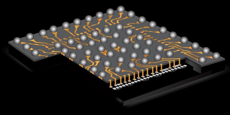
14 M-Series fan-out technology Chips first, chips up fan-out with fully encapsulated active region Planar patterning surface with roadmap to 2µm line & space Adaptive patterning to enable high yields in scaling to tight geometries & low cost die attach Backside Epoxy Silicon Device Cu Stud Cu RDL 1 3 layers Mold Compound Improved reliability with embedded silicon and molded stress buffer Planar Surface Cost-effective solar wafer fab inspired Autoline equipment for 300mm & large panel formats Embedded Chip Note: Multiple patents granted & pending


15 M-Series building blocks Direct Connect Thick Cu Low contact resistance, multi-via capture Polymer Isolated Via Further stress isolation, tighter design rules Multi-Layer, multi-thickness RDL & Dielectrics 5µm lines 5µm Nested Lines 5µm Isolated Line


16 Breaking through the barriers Capital cost breakthrough Solar wafer fab inspired approach Non-fab equipment set Yield & cost breakthrough with Adaptive Patterning Adaptive Alignment* Align the entire RDL pattern to the measured die position Adaptive Routing* Dynamically adapt RDL routing to the measured die position *Note: Multiple patents issued & pending Enables high metal density designs Precisely aligns inductors to the die BGA array fixed to package outline Enables multi-die fan-out


17 M-Series Adaptive Patterning Dual-die application example High frequency SoC Bluetooth radio Adaptive Patterning enables precise fixed pattern alignment for RF devices & adaptive routing for 100% yield for multi-die interconnect Adaptive alignment for RF Adaptive routing for 100% yield


18 Moving from 300mm round to large panel fan-out Wafer Processing Cost 300mm round baseline* 7% 5% 43% 45% Depreciation Materials *Estimated industry average COGS of M-Series with Adaptive Patterning Labor Fac, Ovhd, Other Large panel fan-out has the potential for >30% cost reduction Capital productivity Material efficiency
19 Convergence through M-Series large panel fan-out 7 Technology Cost Comparison (Sales price to customers) 6 6 Cents per mm M-Series large panel fan-out potential Adv Si Analog Si RF Si FC CSP OEM PCB
20 Wafer Foundries SATS EMS
21 Wafer Foundries SATS EMS Fan-out Applications Blurring the Lines SoC Disintegration Apps processor BB Modem RF Combo Single Die Packaging PMIC RF Transceiver Audio Codec EMS-like Modules Wide IO & HB Memory Multi-function RF PoP


22 Convergence of industries Through M-Series fan-out technology


 Large")

23 Convergence through large panel M-Series fan-out in cooperation with ASE Initial Production Future Production 300mm round M-Series Structure* (post chip attach) (post mold & debond) Large panel format M-Series* *Note: Multiple patents issued & pending
24 Thank You
SEMICONDUCTOR TECHNOLOGY -CMOS-
 SEMICONDUCTOR TECHNOLOGY -CMOS- Fire Tom Wada What is semiconductor and LSIs Huge number of transistors can be integrated in a small Si chip. The size of the chip is roughly the size of nails. Currently,
Wafer Thinning and Thru-Silicon Vias
 Wafer Thinning and Thru-Silicon Vias The Path to Wafer Level Packaging jreche@trusi.com Summary A new dry etching technology Atmospheric Downstream Plasma (ADP) Etch Applications to Packaging Wafer Thinning
Layout Analysis Analog Block
 Layout Analysis Analog Block Sample Report Analysis from an HD Video/Audio SoC For any additional technical needs concerning semiconductor and electronics technology, please call Sales at Chipworks. 3685
CMP and Current Trends Related to Advanced Packaging
 CMP and Current Trends Related to Advanced Packaging Robert L. Rhoades, Ph.D. NCCAVS TFUG-CMPUG Joint Meeting June 7, 2017 Semiconductor Equipment Spare Parts and Service CMP Foundry Foundry Click to edit
2016, Amkor Technology, Inc.
 1 Standardization of Packaging for the Internet of Things Adrian Arcedera l VP of MEMS and Sensor Products 2 About Amkor Technology Amkor Technology, Inc. is one of the world's largest and most accomplished
Future trends for SiP In Medical Implant Applications
 Future trends for SiP In Medical Implant Applications Piers Tremlett, Zarlink Semiconductor NMI at TWI, 12 Dec 07 A case study This presentation uses Zarlink s Medical RF device To consider potential embedded
SEMICONDUCTOR TECHNOLOGY -CMOS-
 SEMICONDUCTOR TECHNOLOGY -CMOS- Fire Tom Wada 2011/12/19 1 What is semiconductor and LSIs Huge number of transistors can be integrated in a small Si chip. The size of the chip is roughly the size of nails.
2016, Amkor Technology, Inc.
 1 Standardization of Packaging for the Internet of Things Adrian Arcedera l VP of MEMS and Sensor Products 2 About Amkor Technology Amkor Technology, Inc. is one of the world's largest and most accomplished
InvenSense Fabless Model for the MEMS Industry
 InvenSense Fabless Model for the MEMS Industry HKSTP Symposium Aug 2016 InvenSense, Inc. Proprietary Outline MEMS Market InvenSense CMOS-MEMS Integration InvenSense Shuttle Program and Process MEMS MARKET
Forward-Looking Statements
 Forward-Looking Statements Information in this presentation regarding MagnaChip s forecasts, business outlook, expectations and beliefs are forward-looking statements within the meaning of the Private
Forward-Looking Statements
 Forward-Looking Statements Information in this presentation regarding MagnaChip s forecasts, business outlook, expectations and beliefs are forward-looking statements within the meaning of the Private
Through Silicon Via Testing Known Good Die (KGD) or Probably Good Die (PGD) Doug Lefever Advantest
 or Probably Good Die (PGD) Doug Lefever Advantest") Through Silicon Via Testing Known Good Die (KGD) or Probably Good Die (PGD) Doug Lefever Advantest Single Die Fab Yield will drive Cost Equation. Yield of the device to be stacked 100% 90% 80% Yield of
Through Silicon Via Testing Known Good Die (KGD) or Probably Good Die (PGD) Doug Lefever Advantest Single Die Fab Yield will drive Cost Equation. Yield of the device to be stacked 100% 90% 80% Yield of
Applied Materials. 200mm Tools & Process Capabilities For Next Generation MEMS. Dr Michel (Mike) Rosa
 Rosa") Applied Materials 200mm Tools & Process Capabilities For Next Generation MEMS Dr Michel (Mike) Rosa 200mm MEMS Global Product / Marketing Manager, Components and Systems Group (CSG), Applied Global Services
Applied Materials 200mm Tools & Process Capabilities For Next Generation MEMS Dr Michel (Mike) Rosa 200mm MEMS Global Product / Marketing Manager, Components and Systems Group (CSG), Applied Global Services
Broadcom AFEM-8072 Mid&High Band Front End module in iphone 8/X
 Broadcom AFEM-8072 Mid&High Band Front End module in iphone 8/X RF report by Stéphane ELISABETH February 2018 version 1 2018 by System Plus Consulting Broadcom AFEM-8072 1 Table of Contents 4 o Executive
Enabling Analog Integration. Paul Kempf
 TM Enabling Analog Integration Paul Kempf Overview The New Analog Analog in New Markets Opportunity in Integrated Analog/RF Outsourcing Trends in Analog Enabling Functional Integration Technology Requirements
Nike+ FuelBand SE WM
 Nike+ FuelBand SE WM0110-003 Bluetooth 4.0 Report #17000-140224-NTc Product Description The Nike+ FuelBand SE is a low-energy Bluetooth 4.0-enabled fitness device designed to be worn around the user s
Technology Overview LTCC
 Sheet Code RFi0604 Technology Overview LTCC Low Temperature Co-fired Ceramic (LTCC) is a multilayer ceramic substrate technology that allows the realisation of multiple embedded passive components (Rs,
Leveraging 300 mm Technology Solutions to Enable New MEMS Process Capabilities
 Leveraging 300 mm Technology Solutions to Enable New MEMS Process Capabilities Evan Patton Semicon Europa November 2017 Lam Research Corp. 1 Presentation Outline The Internet of Things (IoT) as a market
9 rue Alfred Kastler - BP Nantes Cedex 3 - France Phone : +33 (0) website :
 website :") 9 rue Alfred Kastler - BP 10748-44307 Nantes Cedex 3 - France Phone : +33 (0) 240 180 916 - email : info@systemplus.fr - website : www.systemplus.fr January 2012 Written by: Maher SAHMIMI DISCLAIMER :
9 rue Alfred Kastler - BP 10748-44307 Nantes Cedex 3 - France Phone : +33 (0) 240 180 916 - email : info@systemplus.fr - website : www.systemplus.fr January 2012 Written by: Maher SAHMIMI DISCLAIMER :
MAXIM INTEGRATED PRODUCTS
 RELIABILITY REPORT FOR PLASTIC ENCAPSULATED DEVICES May 4, 2009 MAXIM INTEGRATED PRODUCTS 120 SAN GABRIEL DR. SUNNYVALE, CA 94086 Approved by Ken Wendel Quality Assurance Director, Reliability Engineering
Perfecting the Package Bare and Overmolded Stacked Dies. Understanding Ultrasonic Technology for Advanced Package Inspection. A Sonix White Paper
 Perfecting the Package Bare and Overmolded Stacked Dies Understanding Ultrasonic Technology for Advanced Package Inspection A Sonix White Paper Perfecting the Package Bare and Overmolded Stacked Dies Understanding
24. Scaling, Economics, SOI Technology
 24. Scaling, Economics, SOI Technology Jacob Abraham Department of Electrical and Computer Engineering The University of Texas at Austin VLSI Design Fall 2017 December 4, 2017 ECE Department, University
Spring Probes and Probe Cards for Wafer-Level Test. Jim Brandes Multitest. A Comparison of Probe Solutions for an RF WLCSP Product
 Session 6 AND, AT THE WAFER LEVEL For many in the industry, performing final test at the wafer level is still a novel idea. While providing some much needed solutions, it also comes with its own set of
High-Performance Technologies for an Analog-Centric World
 High-Performance Technologies for an Analog-Centric World Oct 13, 2011 Lou N. Hutter, SVP GM, Analog Foundry Business Unit Dongbu HiTek Agenda Analog in Our World Today Diverse Technology Needs of the
Meeting the challenge of accurately assembling active optical cables
 More than Precision Meeting the challenge of accurately assembling active optical cables No one would dispute the fact that active optical cable (AOC) and Silicon Photonics technologies are getting tremendous
nmos transistor Basics of VLSI Design and Test Solution: CMOS pmos transistor CMOS Inverter First-Order DC Analysis CMOS Inverter: Transient Response
 nmos transistor asics of VLSI Design and Test If the gate is high, the switch is on If the gate is low, the switch is off Mohammad Tehranipoor Drain ECE495/695: Introduction to Hardware Security & Trust
Overcoming Challenges in 3D NAND Volume Manufacturing
 Overcoming Challenges in 3D NAND Volume Manufacturing Thorsten Lill Vice President, Etch Emerging Technologies and Systems Flash Memory Summit 2017, Santa Clara 2017 Lam Research Corp. Flash Memory Summit
MAXIM INTEGRATED PRODUCTS
 RELIABILITY REPORT FOR EEE+ PLASTIC ENCAPSULATED DEVICES February 18, 2010 MAXIM INTEGRATED PRODUCTS 120 SAN GABRIEL DR. SUNNYVALE, CA 94086 Approved by Ken Wendel Quality Assurance Director, Reliability
Advanced WLP Platform for High-Performance MEMS. Presented by Dean Spicer, Director of Engineering
 Advanced WLP Platform for High-Performance MEMS Presented by Dean Spicer, Director of Engineering 1 May 11 th, 2016 1 Outline 1. Application Drivers for High Performance MEMS Sensors 2. Approaches to Achieving
EE C247B ME C218 Introduction to MEMS Design Spring 2017
 EE C247B ME C218 Introduction to MEMS Design Spring 2017 Prof. Clark T.-C. Nguyen Dept. of Electrical Engineering & Computer Sciences University of California at Berkeley Berkeley, CA 94720 Lecture Module
Because Innovation Matters
 Because Innovation Matters Silicon Systems Group Toru Watanabe President, Applied Materials, Japan Semicon Japan November 30, 2010 Safe Harbor This presentation contains forward-looking statements, including
Semiconductors Displays Semiconductor Manufacturing and Inspection Equipment Scientific Instruments
 Semiconductors Displays Semiconductor Manufacturing and Inspection Equipment Scientific Instruments Electronics 110-nm CMOS ASIC HDL4P Series with High-speed I/O Interfaces Hitachi has released the high-performance
Integrated Circuit Design ELCT 701 (Winter 2017) Lecture 1: Introduction
 Lecture 1: Introduction") 1 Integrated Circuit Design ELCT 701 (Winter 2017) Lecture 1: Introduction Assistant Professor Office: C3.315 E-mail: eman.azab@guc.edu.eg 2 Course Overview Lecturer Teaching Assistant Course Team E-mail:
1 Integrated Circuit Design ELCT 701 (Winter 2017) Lecture 1: Introduction Assistant Professor Office: C3.315 E-mail: eman.azab@guc.edu.eg 2 Course Overview Lecturer Teaching Assistant Course Team E-mail:
MAXIM INTEGRATED PRODUCTS
 RELIABILITY REPORT FOR MAX2135AETN+ PLASTIC ENCAPSULATED DEVICES March 04, 2011 MAXIM INTEGRATED PRODUCTS 120 SAN GABRIEL DR. SUNNYVALE, CA 94086 Approved by Don Lipps Quality Assurance Manager, Reliability
Possible Paths for Cu CMP
 Possible Paths for Cu CMP J.S. Drewery, V. Hardikar, S.T. Mayer, H. Meinhold, F. Juarez, and J. Svirchevski Presented by Julia Svirchevski Agenda Perceived Need for ECMP Technology Differentiation Profile
IEEE TRANSACTIONS ON VERY LARGE SCALE INTEGRATION (VLSI) SYSTEMS, VOL. 23, NO. 2, FEBRUARY
 SYSTEMS, VOL. 23, NO. 2, FEBRUARY") IEEE TRANSACTIONS ON VERY LARGE SCALE INTEGRATION (VLSI) SYSTEMS, VOL. 23, NO. 2, FEBRUARY 2015 317 Scan Test of Die Logic in 3-D ICs Using TSV Probing Brandon Noia, Shreepad Panth, Krishnendu Chakrabarty,
IEEE TRANSACTIONS ON VERY LARGE SCALE INTEGRATION (VLSI) SYSTEMS, VOL. 23, NO. 2, FEBRUARY 2015 317 Scan Test of Die Logic in 3-D ICs Using TSV Probing Brandon Noia, Shreepad Panth, Krishnendu Chakrabarty,
Innovative Fast Timing Design
 Innovative Fast Timing Design Solution through Simultaneous Processing of Logic Synthesis and Placement A new design methodology is now available that offers the advantages of enhanced logical design efficiency
Alien Technology Corporation White Paper. Fluidic Self Assembly. October 1999
 Alien Technology Corporation White Paper Fluidic Self Assembly October 1999 Alien Technology Corp Page 1 Why FSA? Alien Technology Corp. was formed to commercialize a proprietary technology process, protected
Advanced MEMS Packaging
 Advanced MEMS Packaging John H. Lau Chengkuo Lee C. S. Premachandran Yu Aibin Ш New York Chicago San Francisco Lisbon London Madrid Mexico City Milan New Delhi San Juan Seoul Singapore Sydney Toronto Contents
3D-CHIP TECHNOLOGY AND APPLICATIONS OF MINIATURIZATION
 3D-CHIP TECHNOLOGY AND APPLICATIONS OF MINIATURIZATION 23.08.2018 I DAVID ARUTINOV CONTENT INTRODUCTION TRENDS AND ISSUES OF MODERN IC s 3D INTEGRATION TECHNOLOGY CURRENT STATE OF 3D INTEGRATION SUMMARY
Sharif University of Technology. SoC: Introduction
 SoC Design Lecture 1: Introduction Shaahin Hessabi Department of Computer Engineering System-on-Chip System: a set of related parts that act as a whole to achieve a given goal. A system is a set of interacting
RELIABILITY REPORT FOR. MAX6070xxAUTxx+T PLASTIC ENCAPSULATED DEVICES. December 19, 2012 MAXIM INTEGRATED 160 RIO ROBLES SAN JOSE, CA 95134
 RELIABILITY REPORT FOR MAX6070xxAUTxx+T PLASTIC ENCAPSULATED DEVICES December 19, 2012 MAXIM INTEGRATED 160 RIO ROBLES SAN JOSE, CA 95134 Approved by Richard Aburano Quality Assurance Manager, Reliability
The future of microled displays using nextgeneration
 The future of microled displays using nextgeneration technologies Introduction MicroLEDs (micro-light-emitting diodes) are an emerging display technology that, as the name implies, use very small LEDs
MicroLED Displays: Global Trends & Opportunities for Equipment and Material Suppliers
 Picture: Sony From Technologies to Market MicroLED Displays: Global Trends & Opportunities for Equipment and Material Suppliers SEMICON EUROPA Jean-Christophe ELOY - CEO - Yole Développement 2017 AGENDA
SEMI 大半导体产业网
 STATE-OF-THE-ART 3D INTEGRATION GAN HUI, STEVEN OUTLINE Introduction about IMEC Application Areas Driven 3D Integration 3D Integration Technology Conclusions 1 IMEC 1984 2010 1984 Established by state
TKK S ASIC-PIIRIEN SUUNNITTELU
 Design TKK S-88.134 ASIC-PIIRIEN SUUNNITTELU Design Flow 3.2.2005 RTL Design 10.2.2005 Implementation 7.4.2005 Contents 1. Terminology 2. RTL to Parts flow 3. Logic synthesis 4. Static Timing Analysis
P I SCALE Creating an Open Access Flexible O L E D P ilo t L in e S e r vic e
 P I SCALE Creating an Open Access Flexible O L E D P ilo t L in e S e r vic e Pavel Kudlacek pavel.kudlacek@tno.nl P I - SCALE for 2017Flex 1 Lighting c h a lle n g e L ig h t in g c h a lle n g e At least
AIXTRON in EXCILIGHT project
 AIXTRON SE AIXTRON in EXCILIGHT project Gintautas Simkus ABOUT AIXTRON 2 Who we are Headquarter based in Herzogenrath, Germany Worldwide presence with 14 sales/representatives offices and production facilities
I-fuse TM : Best OTP for FD-SOI and Sub-14nm
 I-fuse TM : Best OTP for FD-SOI and Sub-14nm Shine Chung, Chairman May, 2017 Attopsemi Technology 1A2-A1 No. 1 Li-Hsin 1st Rd, Hsinchu, Taiwan 300-76 (886) 3-666-3150x211, (886) 920-566-218 1 1 About Attopsemi
Advancements in Acoustic Micro-Imaging Tuesday October 11th, 2016
 Central Texas Electronics Association Advancements in Acoustic Micro-Imaging Tuesday October 11th, 2016 A review of the latest advancements in Acoustic Micro-Imaging for the non-destructive inspection
MAXIM INTEGRATED PRODUCTS
 RELIABILITY REPORT FOR MAX3639ETM+ PLASTIC ENCAPSULATED DEVICES June 21, 2010 MAXIM INTEGRATED PRODUCTS 120 SAN GABRIEL DR. SUNNYVALE, CA 94086 Approved by Richard Aburano Quality Assurance Manager, Reliability
OPPORTUNITIES IN THE LED LUMINAIRE SUPPLY CHAIN. A Strategic Market and Technology Review
 OPPORTUNITIES IN THE LED LUMINAIRE SUPPLY CHAIN A Strategic Market and Technology Review 2012-2018 Unauthorised copying or distribution of this report to any third party (including associated companies)
Addressing 80 µm pitch Cu Pillar Bump Wafer probing: Technoprobe TPEG MEMS solution
 Addressing 80 µm pitch Cu Pillar Bump Wafer probing: Technoprobe TPEG MEMS solution S. Angles STMicroelectronics R. Vallauri Technoprobe Background Overview ST Qualification of TPEG MEMS T3 probing technology
Title: STMicroelectronics NIR Camera Sensor Pages: 97 Date: December 2017 Format: PDF & Excel file Price: Full report: EUR 3,490
 STMicroelectronics Near Infrared Camera Sensor in the Apple iphone X The first NIR camera sensor with multiple innovations based on imager-silicon-oninsulator substrate from SOITEC, supplied and produced
Scaling up of the Iris AO segmented DM technology for atmospheric correction
 Scaling up of the Iris AO segmented DM technology for atmospheric correction Michael A. Helmbrecht, Ph.D., Min He, Carl Kempf, Ph.D., Patrick Rhodes Iris AO, Inc., 2680 Bancroft Way, Berkeley, CA 94704
EECS150 - Digital Design Lecture 2 - CMOS
 EECS150 - Digital Design Lecture 2 - CMOS January 23, 2003 John Wawrzynek Spring 2003 EECS150 - Lec02-CMOS Page 1 Outline Overview of Physical Implementations CMOS devices Announcements/Break CMOS transistor
High Performance Microprocessor Design and Automation: Overview, Challenges and Opportunities IBM Corporation
 High Performance Microprocessor Design and Automation: Overview, Challenges and Opportunities Introduction About Myself What to expect out of this lecture Understand the current trend in the IC Design
Smart. Connected. Energy-Friendly.
 www.silabs.com Smart. Connected. Energy-Friendly. Miniaturizing IoT Designs Tom Nordman, Pasi Rahikkala This whitepaper explores the challenges that come with designing connected devices into increasingly
RELIABILITY REPORT FOR MAX44241AUA+T PLASTIC ENCAPSULATED DEVICES. September 8, 2014 MAXIM INTEGRATED 160 RIO ROBLES SAN JOSE, CA
 RELIABILITY REPORT FOR MAX44241AUA+T PLASTIC ENCAPSULATED DEVICES September 8, 2014 MAXIM INTEGRATED 160 RIO ROBLES SAN JOSE, CA 95134 Approved by Eric Wright Quality Assurance Reliability Engineering
Multi-Shaped E-Beam Technology for Mask Writing
 Multi-Shaped E-Beam Technology for Mask Writing Juergen Gramss a, Arnd Stoeckel a, Ulf Weidenmueller a, Hans-Joachim Doering a, Martin Bloecker b, Martin Sczyrba b, Michael Finken b, Timo Wandel b, Detlef
MARKET OUTPERFORMERS CELERITAS INVESTMENTS
 MARKET OUTPERFORMERS CELERITAS INVESTMENTS Universal Displays (OLED) Rating: Strong Buy Stock Price: $101/share Price Target: $130/share MOP Idea of the Month: Universal Displays Business Overview: Universal
Overcoming challenges of high multi-site, high multi-port RF wafer sort testing
 June 7-10, 2009 San Diego, CA Overcoming challenges of high multi-site, high multi-port RF wafer sort testing Daniel Watson Mechanical Engineer Teradyne, nc. Worldwide RF Semiconductor Market Trends: Strong
UV Nanoimprint Tool and Process Technology. S.V. Sreenivasan December 13 th, 2007
 UV Nanoimprint Tool and Process Technology S.V. Sreenivasan December 13 th, 2007 Agenda Introduction Need tool and process technology that can address: Patterning and CD control Alignment and Overlay Defect
Imperial College OF SCIENCE, TECHNOLOGY AND MEDICINE University of London. Digital IC Design Course
 Scalable CMOS Layout Design Rules Scalable CMOS Layout Design Rules Imperial College OF SCIENCE, TECHNOLOGY AND MEDICINE University of London Department of Electrical & Electronic Engineering Digital IC
STMicroelectronics Standard Technology offers at CMP in 2017 Deep Sub-Micron, SOI and SiGe Processes
 STMicroelectronics Standard Technology offers at CMP in 2017 Deep Sub-Micron, SOI and SiGe Processes http://cmp.imag.fr STMicroelectronics Technology offers at CMP: 160nm CMOS: BCD8SP 1994 at CMP 160nm
IoT Technical foundation and use cases Anders P. Mynster, Senior Consultant High Tech summit DTU FORCE Technology at a glance
 IoT Technical foundation and use cases Anders P. Mynster, apm@force.dk Senior Consultant High Tech summit DTU 2017 FORCE Technology at a glance Internet of Things devices everywhere! Gartners Hype cycle
SoC Development and DFT Strategy in nano-scale Era
 SoC Development and DFT Strategy in nano-scale Era Woo-Hyun Paik ( 白佑鉉 ) paikwh@lge.com System IC Division LG Electronics Outline System and SoC Trends Role of SoC SoC Design Challenges DFT Issues DFT
MAXIM INTEGRATED PRODUCTS
 RELIABILITY REPORT FOR MAX3580ETJ+ PLASTIC ENCAPSULATED DEVICES January 19, 2009 MAXIM INTEGRATED PRODUCTS 120 SAN GABRIEL DR. SUNNYVALE, CA 94086 Approved by Ken Wendel Quality Assurance Director, Reliability
PROCESS TECHNOLOGIES FOR ADVANCED ORGANIC ELECTRONIC DEVICES: MICRODISPLAYS, LIGHTING AND SOLAR CELLS
 PROCESS TECHNOLOGIES FOR ADVANCED ORGANIC ELECTRONIC DEVICES: MICRODISPLAYS, LIGHTING AND SOLAR CELLS Dr. Christian May Fraunhofer IPMS - Center for Organic Materials and Electronic Devices Dresden COMEDD
Broken Scan Chains Routinely Debugged with New Optical Technique
 t a m V- 3000.0 2500.0 2000.0 1500.0 1000.0 500.0 0.00-500.0-1000.0-1500.0 OSCILLOSCOPE Design file: MSFT DIFF CLOCK WITH TERMINATORREV2.FFS Designer: Microsoft HyperLynx V8.0 Comment: 650MHz at clk input,
DEPFET Active Pixel Sensors for the ILC
 DEPFET Active Pixel Sensors for the ILC Laci Andricek for the DEPFET Collaboration (www.depfet.org) The DEPFET ILC VTX Project steering chips Switcher thinning technology Simulation sensor development
SoC IC Basics. COE838: Systems on Chip Design
 SoC IC Basics COE838: Systems on Chip Design http://www.ee.ryerson.ca/~courses/coe838/ Dr. Gul N. Khan http://www.ee.ryerson.ca/~gnkhan Electrical and Computer Engineering Ryerson University Overview SoC
projectors, head mounted displays in virtual or augmented reality use, electronic viewfinders
 Beatrice Beyer Figure 1. (OLED) microdisplay with a screen diagonal of 16 mm. Figure 2. CMOS cross section with OLED on top. Usually as small as fingernails, but of very high resolution Optical system
NOTES: Dimensions are in mm (inches) Tolerances are +/ (0.010) unless otherwise stated.
 Tolerances are +/ (0.010) unless otherwise stated.") Bright Red MST4110C, MST4140C High Efficiency Red MST4910C, MST4940C Green MST4410C, MST4440C TR/QTS/030100-001 PACKAGE DIMENSIONS FEATURES Bright Bold Segments Common Anode/Cathode Low Power Consumption
Bright Red MST4110C, MST4140C High Efficiency Red MST4910C, MST4940C Green MST4410C, MST4440C TR/QTS/030100-001 PACKAGE DIMENSIONS FEATURES Bright Bold Segments Common Anode/Cathode Low Power Consumption
A pixel chip for tracking in ALICE and particle identification in LHCb
 A pixel chip for tracking in ALICE and particle identification in LHCb K.Wyllie 1), M.Burns 1), M.Campbell 1), E.Cantatore 1), V.Cencelli 2) R.Dinapoli 3), F.Formenti 1), T.Grassi 1), E.Heijne 1), P.Jarron
ABSTRACT 1 INTRODUCTION
 Novel lithography technique using an ASML Stepper/Scanner for the manufacture of display devices in MEMS world ASML US, Inc Special Applications, 6580 Via Del Oro San Jose, CA 95119 Keith Best, Pankaj
High Speed Digital Design Seminar
 High Speed Digital Design Seminar Introduction to Black Magic, with Dr. Howard Johnson About this course Printable Index 1. Vocabulary of Signal Integrity High Speed Digital Design: Opening Lecture. HSDD
Semiconductor Devices. Microwave Application Products. Microwave Tubes and Radar Components
 Microwave Application Products Microwave Tubes and Radar Components Our semiconductor products are mostly analog semiconductors classified broadly into three groups: Bipolar ICs, MOS ICs, and Microwave
(12) Patent Application Publication (10) Pub. No.: US 2009/ A1
 Patent Application Publication (10) Pub. No.: US 2009/ A1") US 200901 22515A1 (19) United States (12) Patent Application Publication (10) Pub. No.: US 2009/0122515 A1 O0n et al. (43) Pub. Date: May 14, 2009 (54) USING MULTIPLETYPES OF PHOSPHOR IN Related U.S. Application
US 200901 22515A1 (19) United States (12) Patent Application Publication (10) Pub. No.: US 2009/0122515 A1 O0n et al. (43) Pub. Date: May 14, 2009 (54) USING MULTIPLETYPES OF PHOSPHOR IN Related U.S. Application
Monolithic Optoelectronic Integration of High- Voltage Power FETs and LEDs
 Monolithic Optoelectronic Integration of High- Voltage Power FETs and LEDs, Zhongda Li, Robert Karlicek and T. Paul Chow Smart Lighting Engineering Research Center Rensselaer Polytechnic Institute, Troy,
EQUIPMENT COATING SYSTEMS FOR THIN-FILM PV THIN-FILM PHOTOVOLTAICS. SCALA VISS PIA nova GC120VCR XENIA
 THIN-FILM PHOTOVOLTAICS EQUIPMENT COATING SYSTEMS FOR THIN-FILM PV SCALA VISS PIA nova GC120VCR XENIA OUR STORY. OUR EXPERIENCE. RANGE OF APPLICATIONS VON ARDENNE provides advanced PVD coating equipment
Achieving Faster Time to Tapeout with In-Design, Signoff-Quality Metal Fill
 White Paper Achieving Faster Time to Tapeout with In-Design, Signoff-Quality Metal Fill May 2009 Author David Pemberton- Smith Implementation Group, Synopsys, Inc. Executive Summary Many semiconductor
Low Power Design: From Soup to Nuts. Tutorial Outline
 Low Power Design: From Soup to Nuts Mary Jane Irwin and Vijay Narayanan Dept of CSE, Microsystems Design Lab Penn State University (www.cse.psu.edu/~mdl) ISCA Tutorial: Low Power Design Introduction.1
LCOS for Large-Screen HDTV
 LCOS for LargeScreen HDTV BOB MELCHER, CTO JULY 28, 2004 LCOS HDTV 2 Agenda What is the opportunity for microdisplay HDTVs? Why are LCOS microdisplays the preferred technology for highperformance HDTV?
ESE534: Computer Organization. Previously. Today. Previously. Today. Preclass 1. Instruction Space Modeling
 ESE534: Computer Organization Previously Instruction Space Modeling Day 15: March 24, 2014 Empirical Comparisons Previously Programmable compute blocks LUTs, ALUs, PLAs Today What if we just built a custom
Advanced Display Manufacturing Technology
 Advanced Display Manufacturing Technology John Busch Vice President, New Business Development Display and Flexible Technology Group September 28, 2017 Safe Harbor This presentation contains forward-looking
Benchtop Portability with ATE Performance
 Benchtop Portability with ATE Performance Features: Configurable for simultaneous test of multiple connectivity standard Air cooled, 100 W power consumption 4 RF source and receive ports supporting up
ECTC in Las Vegas. What happens in Las Vegas at ECTC, doesn t stay in Las Vegas, it is shared here.
 ECTC in Las Vegas By Sandra Winkler, Senior Industry Analyst, New Venture Research, www.newventureresearch.com Photos taken at the conference are posted on Flickr: http://www.flickr.com/photos/38916807@n07/sets/72157633891833244/
Structure, Process & Cost Analysis
 Reverse Costing Structure, Process & Cost Analysis Heimann Sensor 32 x 32-array thermopile LWIR image sensor with silicon lens A small, easy to use, low-power, cheap non-contact temperature measurement
Course Title: High-Speed Wire line/optical Transceiver Design
 Course Title: High-Speed Wire line/optical Transceiver Design Course Outline Introduction to Serial Communications Wire line Transceivers Transmitters Receivers Optical Transceivers Transimpedance Amplifiers
IC TECHNOLOGY Lecture 2.
 IC TECHNOLOGY Lecture 2. IC Integrated Circuit Technology Integrated Circuit: An integrated circuit (IC, a chip, or a microchip) is a set of electronic circuits on one small flat piece (or "chip") of semiconductor
Application Note. 3G SDI Evaluation Board. Revision Date: July 2, 2009
 3G SDI Evaluation Board Revision Date: July 2, 2009 Copyrights and Trademarks Copyright 2009 Samtec, Inc. Copyright 2009 Brioconcept Consulting Developed in collaboration between Samtec, Inc Brioconcept
New Worlds for Polymers: Organic Transistors, Light Emitting Diodes, and Optical Waveguides Ed Chandross
 New Worlds for Polymers: Organic Transistors, Light Emitting Diodes, and Optical Waveguides Ed Chandross Materials Chemistry, LLC 1 Polymers in the Electronic Industry Enabling Materials Active Materials?
SINGULATION BY PLASMA ETCHING. INTEGRATION TECHNIQUES TO ENABLE LOW DAMAGE, HIGH PRODUCTIVITY DICING.
 SINGULATION BY PLASMA ETCHING. INTEGRATION TECHNIQUES TO ENABLE LOW DAMAGE, HIGH PRODUCTIVITY DICING. Richard Barnett Dave Thomas Oliver Ansell ABSTRACT Plasma dicing has rapidly gained traction as a viable
Flexible Electronics Production Deployment on FPD Standards: Plastic Displays & Integrated Circuits. Stanislav Loboda R&D engineer
 Flexible Electronics Production Deployment on FPD Standards: Plastic Displays & Integrated Circuits Stanislav Loboda R&D engineer The world-first small-volume contract manufacturing for plastic TFT-arrays
Implementation Challenges and Solutions of Low-Power, High-Performance Memory Systems
 WHITE PAPER Implementation Challenges and Solutions of Low-Power, High-Performance Memory Systems 1050 Enterprise Way, Suite 700 Sunnyvale, CA 94089 Phone: + 1 408 462 8000 Fax: + 1 408 462 8001 www.rambus.com
Challenges for OLED Deposition by Vacuum Thermal Evaporation. D. W. Gotthold, M. O Steen, W. Luhman, S. Priddy, C. Counts, C.
 Challenges for OLED Deposition by Vacuum Thermal Evaporation D. W. Gotthold, M. O Steen, W. Luhman, S. Priddy, C. Counts, C. Roth June 7, 2011 Outline Introduction to Veeco Methods of OLED Deposition Cost
ADDING AN O TO LEDS STATUS AND PERSPECTIVES OF ORGANIC LIGHT EMITTING DIODES PAWEL E. MALINOWSKI, TUNGHUEI KE LED EVENT 2017
 ADDING AN O TO LEDS STATUS AND PERSPECTIVES OF ORGANIC LIGHT EMITTING DIODES PAWEL E. MALINOWSKI, TUNGHUEI KE LIVING ROOM NOT SO LONG AGO... 2 Source: Warner Bros. Incadescent CRT 3 Source: Warner Bros.
Reliability of Level 1 and Level 2 Packaging in Solid-State Lighting Devices
 Reliability of Level 1 and Level 2 Packaging in Solid-State Lighting Devices Lynn Davis, PhD Fellow, RTI International December 8, 2016 1 RTI International is a registered trademark and a trade name of
Generating Spectrally Rich Data Sets Using Adaptive Band Synthesis Interpolation
 Generating Spectrally Rich Data Sets Using Adaptive Band Synthesis Interpolation James C. Rautio Sonnet Software, Inc. WFA: Microwave Component Design Using Optimization Techniques June 2003 Interpolation