Test-Pattern Compression & Test-Response Compaction. Mango Chia-Tso Chao ( 趙家佐 ) EE, NCTU, Hsinchu Taiwan
|
|
|
- Sheila Tate
- 6 years ago
- Views:
Transcription
1 Test-Pattern Compression & Test-Response Compaction Mango Chia-Tso Chao ( 趙家佐 ) EE, NCTU, Hsinchu Taiwan
2 Outline Introduction to Scan-based Testing Input-Pattern Compression Type of compressions Compression schemes Low-power decompression Output-Response Compaction Time compactor (MISR) Unknown-tolerant compaction schemes Diagnosis with compactor Design Optimal Space Compactor Hybrid Compaction Scheme Conclusion
3 Scan-based Testing Input Pattern PIs PPIs Combinational Circuit POs PPOs Output Response Good-circuit response + Good? Scan-in Pattern Flip-flops Scan-out Response Advantage of scan Better controllabilityand observability, lower ATPG complexity, higher fault coverage Disadvantage of scan Long test-application time and large test-data volume

4 Input-Stimulus Compression & Output-Response Compaction Break a long scan chain into several short ones Still use limited ATE channels to supply test patterns and observe responses Save test-application time and test-data volume
5 IC/Tester Performance Comparison No. of transistors IC Frequency 1KHz 1MHz 10MHz 20MHz 300MHz 1GHz Figure of merit x x Tester pins ATE Frequency 1KHz 200KHz 10MHz 80MHz 400MHz 800MHz Figure of merit x x10 9 2x X X10 12
6 IC/Tester Performance Comparison
7 Ideal Compression/Compaction Scheme No modification to functional logic Such as test point insertion ATPG independent Need not buy a new ATPG Pattern independent hardware Changing test set need not changing hardware No coverage loss Target fault model & un-modeled faults Small area overhead
8 Outline Introduction to Scan-based Testing Input-Pattern Compression Type of compressions Compression schemes Output-Response Compaction Time compactor (MISR) Unknown-tolerant compaction schemes Diagnosis with compactor Design optimal space compactor Hybrid compaction scheme Conclusion
9 Pattern Compression vs. Compaction Compaction less # of test vectors but still the same fault coverage Compactable test cubes Pattern re-ordering (due to fault dropping order) 1XXXX0XX1 11XXXXX0X X1X0XXX0X X011X1XXX 00XXXXX00 11X0X0X X1X00 pttn 1 pttn fault lists Compression less # of bits per test vector pttn n
10 Vertical Compression vs. Horizontal Compression Vertical compression Store one seed to supply multiple different patterns # of seeds < # of deterministic patterns # of applied patterns > # of deterministic patterns Folding sequence [Liang ITC 01], XWork[NEC patent] Mostly used in BIST architecture deterministic pttn seed decompress applied pttn Horizontal compression Length of a seed < length of a pattern
11 Input Compression Schemes Coding Strategy Huffman coding, Run-length variable coding, Statistical coding LFSR Reseeding Static reseeding, dynamic reseeding Broadcasting Illinois Scan, reconfigurable switch Continuous-Flow Linear Expansion SmartBist, Linear Network Mutation Random access scan Low-power decompression scheme low-power EDT
12 Run-Length Coding WWWWWWWWWWWWBWWWWWWWWWWWWBB BWWWWWWWWWWWWWWWWWWWWWWWWB WWWWWWWWWWWWWW 12WB12W3B24WB14W Burrows-Wheeler transform can be used to maximize the run length

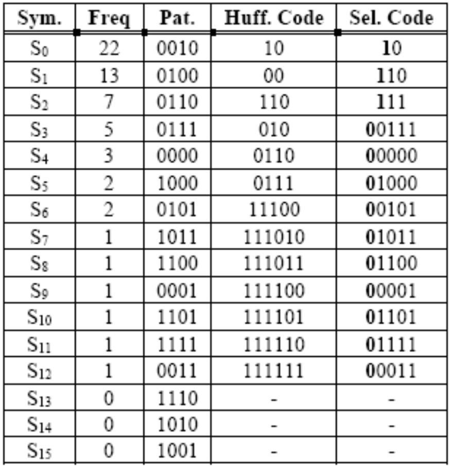
13 Statistical Coding ref: [Jas VTS 99]


14 LFSR Reseeding Linear Feedback Shift Register System of linear equations Test Cube = 1 X X X 0 1 X X 1 0 Ref: [Konemann ETC 91]
15 LFSR Reseeding Periodically Reseeding -The LFSR size has to be large enough to achieve low probability (<10-6 ) of not finding a seed Single-polynomial LFSR : > Maximum specified bits (Smax) + 20 LFSR-Coded Test Patterns for Scan Design, Konemann ETC 91 Multiple-polynomial LFSR : > Smax+ 4 Generation of vectors patterns through reseeding of multiplepolynomial LFSR, S. Hellebrand. et.al, ITC 92 Dynamic reseeding Seed is modified incrementally while test generation proceeds Test Vector Encoding Using Partial LFSR Reseeding, C.V.Krishna, ITC 01
16 Broadcasting Illinois Scan One scan line is routed to multiple scan chains A case study on the implementation of Illinois scan architecture, Hsu, et.al, ITC 01

17 Continuous-flow Linear Expansion Use Xor- or inverter- network for de-compression A SmartBIST Variant with Guaranteed Encoding, Koenemann, ATS 01 Frugal Linear Network-Based Test Decompression for Drastic Test Cost Reductions, Rao ICCAD
18 Mutation Supply the current pattern by flipping bits of the last pattern Input test-data n Decoder Shift Registers (DSR) Enable n To 2 n n x 2 decoder scan chains Decoder Output Registers (DOR) Ref: [Reda DATE 02]
19 Mutation State transition diagram of DSR 0 Distance matrix for state transition diagram
20 Mutation Circular scan Flip the bits from the captured values Scan Selection Inputs (N-1) 1 pin Data Input Decoder ( N-1 x 2 N-1 ) 2 N-1 Scan Chains Decoder Output Scan Output MUX Data Input Output Compactor Scan Input Ref: [Arslan ICCAD 04]


21 Industrial Tools Synopsys: XDBIST LFSR reseeding shadow LFSR seed LFSR Mentor Graphics: TestKompress (EDT) Test cubes are compacted prior to random fill, random fill is achieved through decompression
22 TestKompress Injector Ring Generator 4 6 Phase Shifter cycle V0 0 3 L 6

23 TestKompress System of linear equations cycle cycle Test cubes cycle
24 LFSR Reseeding vs. Ring Generator LFSR Reseeding LFSR depth (seed length) is determined by the pattern with most specified bits Attempt to lower the most specified bits of a pattern rather than average specified-bit % specified bits Ring generator pttn specified bits An input bit determines outputs for d(depth) cycles Ring depth is determined by the congestion of specified bits over a period of time pttn ring input ring output : inputs to supply specified bits : specified bits
25 Low-power Decompression Scheme More scan cells lead to higher power consumption during scan-shifting Attempt to minimize scan-value switching during decompression Mutation-based decompression is good for lowpower scan testing but low compression ratio LFSR reseeding or ring generator may achieve high compression ratio but produce a lot switching due to random-fill nature Recent low-power decompression schemes Low Power EDT (DAC 07)
26 Low-Power EDT (1/3) The basic EDT-based decompressor randomly fill the unspecified bits. Main idea is to reduce the fill rate. Let successive unspecified bits have the same value Need a mechanism to sustain the outputs of a decompressor for more than a single clock cycle


27 Low-Power EDT (2/3) A shadow registercan save the preceding decompression information and set a desired state of ring generator Need additional channel to control shadow register Merge control bits with original input channels
28 Low-Power EDT (3/3) To further reduce the switching activity, it partitions the original test cube into several blocks comprising consecutive slices Allow one to repeat a given decompressorstate many times in succession The actual block size is determined by the ability to encode the specified bits occurring within boundaries of the block As a result, we can achieve virtually the smallest number of blocks that cover the entire test cube block 1 block 2 block 3 block 4 block 5
29 Outline Introduction to Scan-based Testing Input-Pattern Compression Type of compressions Compression schemes Output-Response Compaction Time compactor (MISR) Unknown-tolerant compaction schemes Diagnosis with compactor Design optimal space compactor Hybrid compaction scheme Conclusion
30 Output-Response Compaction Key barrier to effective test response compaction: unknown values among good-circuit results If no unknown value, MISR(Multiple Input Signature Registers) can compress an infinitely long output sequence into a fixed-length signature
31 Unknown Values Definition: the good-circuit response which cannot be calculated by the simulator Source of unknown values Un-initialized flip-flops Bus contention Floating bus Multi-cycle paths Limitation of simulator Low percentage of unknown (less than 1%) for most industrial designs
32 Unknown-Tolerant Compaction Scheme Selective compactor Unknown-blocking MISRs Space compactor Hybrid compaction scheme
33 Unknown-Tolerant Compaction (1/3) Selective Compactor Observe only the responses with faulty value Discard majority of the responses Required a customized ATPG [Wohl, ITC 03], [Mentor Graphics, EDT] output 1 output 2 output 16 8-to-1 8-to-1 8-to-1 (1) 16-to-1 (2) 16-to-1 (64) 16-to-1 scan chain 1 scan chain 2.. Ref: [Synopsys, XDBIST] scan chain 512
34 Control Signals for XDBIST selector shadow si0 si1 si Selector control (160 bits) sel 0 sel 1 sel 2 64 x 2-input XOR 64 x 2-input XOR 64 x 2-input XOR sel 3 sel 4 sel x 2-input XOR 64 sel 6 si3 512 scan chains
35 Unknown-Tolerant Compaction (2/3) Unknown-Blocking MISR Block unknowns before feeding into a time compactor [Pomeranz, TCAD 04], [Tang, ITC 04], [Chickermane, ITC 04] Required pattern-dependent blocking logic or customized ATPG Over-mask some known responses scan chain f u S1 0 : must-observe 1 : blocking (for unknown) f scan chain u scan chain u S2 S3 MISR cycle S1 S2 S3 4 x x 0 3 x 1 x 2 0 x x x around 50% of the scan-out responses will be blocked!!
36 Unknown-Tolerant Compaction (3/3) Space Compactor Allow unknown values propagating to the compactor UseXormatrixto reduce the probability that a response is masked by unknowns Pattern-independent HW, APTG-independent flow Single-weight Xor matrix X-compact [Mitra, TCAD 02] Multiple-weight Xor matrix [Clouqueur ITC 05] Xor network with storage elements Block compactor [Wang, ICCAD 03] Convolution compactor, Rajski ITC 03
37 Masking Effects Using XOR Matrix Error masking (aliasing) Error (e): different response from good-circuit response Unknown-induced masking Unknown (u): unknown response in simulation scan chain scan chain e + u + + no error observed + always unknown e + e + + +
38 X-Compact 5 output XOR Matrix scan chain scan chain scan chain scan chain scan chain scan chain scan chain scan chain scan chain scan chain No identical column Odd # of 1s for each column Can observe 1, 2, or any odd # of errors in the same cycle Can observe any 1 error in presence of any 1 unknown
39 X-Compact canceled canceled observable observable :error
40 X-Compact canceled canceled canceled canceled canceled :error
41 X-Compact X X X X X :unknown value :observable value :unobservable value X X
42 Block Compactor output clock CS When CS=1, FF captures response from XOR matrix When CS=0, FF captures response from the FF below it CS A1 A2 A3 A4 A5 B1 B2 B3 B4 B5 The same guarantee for error masking & unknown masking as X-Compact Any compaction ratio for any # of scan chains & any # of outputs scan chain A scan chain B
43 Convolution Compactor output XOR Matrix = 1 = Same guarantee of error masking and unknown masking with X-Compact Any compaction ratio for any # of scan chains & any # of outputs scan chain scan chain scan chain scan chain scan chain scan chain Best compaction ratio/hardware overhead
44 Convolution Compactor Cycle N+2: N+3: N: N+1: Map Shift Shift Map X X X X : unknown value : error X
45 Diagnosis with Compaction Schemes? Selective compactor: Report exact position of erroneous responses, i.e., which scan cell captures erroneous response on which pattern Some erroneous responses may miss Unknown-blocking MISR: All erroneous responses mix together, worst resolution Report only pass or fail Space compactor: Unique faulty syndrome for single error (when no unknown) Lower resolution when multiple errors occur Good for fault-dictionary-based diagnosis Suggestion: Should design a by-pass modein the compaction scheme so that the complete erroneous information can be collected when needed
46 Outline Introduction to Scan-based Testing Input-Pattern Compression Type of compressions Compression schemes Output-Response Compaction Time compactor (MISR) Unknown-tolerant compaction schemes Diagnosis with compactor Design optimal space compactor Hybrid compaction scheme Conclusion
47 X-induced Masking When multiple unknown values appear Some known responses become unobservable Exemplary 20-to-6 X-Compactor X X : unknown value : unobservable response outputs X X X X x-infected outputs X X scan chains
48 X-induced Masking When multiple unknown values appear Some known responses become unobservable Exemplary 20-to-6 X-Compactor X X : unknown value : unobservable response outputs X X X X x-infected outputs X X scan chains
49 Objectives Estimate observable percentage: percentage of responses being observable in presence of unknowns Design a space compactor with maximal compaction ratio and desired observable percentage Relate observable percentage to test-quality metric Stuck-at-fault coverage, Bridge Coverage Estimate (BCE)
50 X-induced Masking vs. Error Masking Error masking: multiple errors cancel one another out by Xor operations Simple experiment: 50-to-1 simple Xor tree Circuit det flt w/o compactor aliaing flt for a pttn aliasing flt % un-det flt with compactor s s s b Error masking barely affects fault detection, but unknown-induced masking does!
51 Construction Rule for Xor Matrix X-Compact requires: Unique columnsin Xor matrix Odd numberof Xor gates for each column (weight) These two rule only help reducing error masking We focus on reducing X-induced masking: Allow identical columns Allow even number of weight
52 Input/Output Parameters for Equation of Observable Percentage Inputs parameters: W: # of Xor gate per column M : # of outputs p : unknown % among responses S : # of responses from scan chains Output: UP (unobservable percentage) % of responses masked by unknown values OP (observable percentage): 1-UP
53 General Concept of our Mathematical Derivation unknowns (N) unknown-infected outputs (K) unobservable responses Xor matrix responses from compactor s input (S) outputs (M)
54 Mathematical Derivation Step 1 Given # of unknowns (N ), the probabilitythat K outputs are x-infected is: K x-infected outputs X X X X X X X Nunknowns
55 Mathematical Derivation Step 2 Given K x-infected outputs, the probability that a response is unobservable is : Its expectation: K x-infected outputs X X X X X : unobservable response X X
56 Mathematical Derivation Step 3 # of unknowns at inputs (N ) is a random variable So, we re-express the E[f(K)] as a function of N, then the unobservable percentage (UP) is:
 Changing weight 10 outputs, 100 scan chains, 1% unknown")
57 Accuracy Comparison Compare prediction results with simulation results 1-million sampling of biased unknowns(90% unknowns come from 10% chains) Changing weight 10 outputs, 100 scan chains, 1% unknown


58 Accuracy Comparison Change other parameters Changing unknown % 10 output 100 scan chains weight of 3 Changing # of chain 10 output weight of 3 1% unknown
59 Designing An Optimal Compactor Given: desired observable %, unknown %, # of outputs Find: S : maximal # of supported scan chains W : optimal weight # of chain observable % w=1 w=2 w= output 1% unknown 90% desired obs.% max_chain = 240, W = 2
60 How Much Observable Percentage Is Enough? Test-quality metrics used in this work stuck-at-fault coverage, BCE [Benware ITC 03] Test quality w.r.t an observable % highly depends on test set and circuit under test obs. % 10% 30% 50% 70% 90% 95% 100% b s s s Stuck-at fault coverage w.r.t. observable percentages
61 Test-Quality Prediction (Stuck-at-fault Coverage & BCE) Inputs CUT, test set, a list of observable percentages(op s) Outputs Stuck-at-fault coverage& BCE for each op Approach: For each fault f, we collect the following statistics DN f : total # of patterns detecting fault f (detecting patterns) ON f : total # of outputs propagating a faulty value of f for entire test set (faulty outputs) One-time fault-simulation-based method for all op s
62 Prediction of Stuck-at-fault Coverage The probability that a fault can be detected under a given op : Then, the predicted fault coverage (FC) is:
63 Prediction of BCE Definition: N f is the # of patterns detecting f (N f = DN f, when op= 1.0) For each fault f, we approximate# of outputs containing faulty value for each detecting pattern by its average: ON f /DN f Probability (a f ) that a detecting pattern still detects f is: # of detecting patterns for a fault f is a binomial distribution, 0<N f <DN f
64 Prediction of BCE (cont d) Expectation of the BCE function for a fault f: The predicted BCE for a given opis
65 Accuracy Comparison for Stuck-at-fault Coverage Prediction ckt B17 s35932 s38417 s38584 obs % Avg. sim. cov prd. cov error sim. cov prd. cov error sim. cov prd. cov error sim. cov prd. cov error
66 Accuracy Comparison for BCE Prediction ckt b17 s35932 s38417 s38584 obs % Avg. sim. BCE prd. BCE error sim. BCE prd. BCE error sim. BCE prd. BCE error sim. BCE prd. BCE error
67 Runtime of the Test-Quality Prediction Compare the runtime between our prediction scheme and a BCE fault simulation ckt BCE sim. (a) 20-op prd. (b) 40-op prd. (c) (b) -(a) (c) (b) b s s s
68 Outline Introduction to Scan-based Testing Input-Pattern Compression Type of compressions Compression schemes Output-Response Compaction Time compactor (MISR) Unknown-tolerant compaction schemes Diagnosis with compactor Design optimal space compactor Hybrid compaction scheme Conclusion
69 Unknown-Blocking MISR Block unknowns before feeding into a time compactor Pomeranz TCAD 04, Tang ITC 04, Chickermane ITC 04 Required pattern-dependent blocking logic or customized ATPG Over-mask some useful responses scan chain f u S1 0 : must-observe 1 : blocking (for unknown) f scan chain u scan chain u S2 S3 MISR cycle S1 S2 S3 4 x x 0 3 x 1 x 2 0 x x x around 50% of the scan-out responses will be blocked!!
70 Coverage Loss with Different % of Observable Responses circuit # of # of must-obs total detected BCE pttn scan FF res. % tran. flt tran. flt s s s b circuit must-obs. only observable percentage 50% 60% 70% 80% 90% 95% s s s b Avg Transition fault coverage loss
71 Coverage Loss with Different % of Observable Responses circuit must-obs. only observable percentage 50% 60% 70% 80% 90% 95% s s s b Avg BCE loss
72 Hybrid Compaction Scheme using Space Compactor & X-blocking MISR seed scan chains LFSR unknown-blocking MISR Our objective 1. ATPG-independent flow Blocking Logic MISR 2. Pattern-independent HW 3. Full model-fault coverage 4. Desired observable % Space Compactor compacted results 5. Maximal # of scan chains 6. Minimal test data
73 Input/Output of the Design Flow for Hybrid Compaction Scheme Input CUT, test set, and target fault model of the test set # of ATE channels (ATE_out ) used for space compactor Desired observable % for the whole compaction scheme (target_obs_p) Desired observable % for the space compactor (space_obs_p) space_obs_p = 2*target_obs_p 1 Output Space compactorwith max number of scan chains (max_chain) & optimal weight(w) Blocking logicfor the test responses and its LFSR seeds for the control signals of the blocking logic
74 Reversed-order Fault Simulation for Must-observe Responses pattern 1 pattern 2 pattern 3.. pattern n-2 pattern n-1 pattern n Target fault lists f a f a+1 f a+2 u Minimize the # of mustobserve responses Reversed-order f 1 fault simulation f 1 f 2 u f 1 f 2
75 Coverage and Test-Data Comparison on s ATE channels for space compactor, 0.5% unknown, 1730 scan cells 90% desired observable percentage Actual obs. % Tran. flt cov. loss (%) BCE loss (%) Hybrid scheme X-blocking only Coverage loss comparison Space compactor LFSR Total Compaction ratio Hybrid scheme X-blocking only _ Test data comparison
76 Coverage-Loss Comparison Hybrid compaction scheme can always achieve lower coverage loss for the un-modeled faults s38417 s38584 b17 Actual obs. % Tran. flt cov. loss (%) BCE loss (%) Hybrid X-blocking only Hybrid X-blocking only Hybrid X-blocking only Coverage loss comparison
77 Test Data Comparison Higher observable percentage may not require higher test data s38417 s38584 b17 Space compactor LFSR Total Compact ratio Hybrid X X-blocking only _ X Hybrid X X-blocking only _ X Hybrid X X-blocking only _ X Test data comparison
78 Compaction Ratio for Different Unknown Percentages Compaction ratioof hybrid schemeincreases more significantlythan using X-blocking MISR, when the unknown percentage goes down Unknown percentage 0.5 % 0.3 % 0.1 % s35932 s38417 s38584 b17 Hybrid 22.0 x 36.6 x 41.8 x X-blocking only 8.3 x 8.4 x 9.2 x Hybrid 24.9 x 39.6 x 60.1 x X-blocking only 54.4 x 62.2 x 72.6 x Hybrid 27.9 x 40.2 x 64.1 x X-blocking only 22.2 x 22.5 x 26.6 x Hybrid 23.3 x 28.0 x 39.8 x X-blocking only 26.1 x 27.5 x 28.5 x Compaction ratio comparison
79 Comparison to Space Compactors Circuit comp. ratio s x s x s x b x method # of channel s.a. cov. loss (%) tran. cov loss (%) BCE loss (%) Hybrid X-comp Hybrid X-comp Hybrid X-comp Hybrid X-comp
80 Experimental Results for Industrial Designs Circuit # of scan FFs Gate count # of test patterns ATPG-detected fault D K 542 (3063) D K 1514 (25859) Overhead Original area Space comp. X-block MISR Total area Overhead % Runtime (sec) D D Coverage loss Actual obs. % Tran. flt cov. loss (%) BCE loss (%) Compaction ratio D D
81 Prediction of BCE for Hybrid Compaction Scheme For each fault f, we collect the following statistics DN f : total # of patterns detecting fault f (detecting patterns) ON f : total # of outputs propagating a faulty value of f for entire test set (faulty outputs) Hybrid compaction scheme guarantee at least one detectionfor the stuck-at fault, N f cannot be 0., 0 < N f <DN f
82 Prediction of BCE for Hybrid Compaction Scheme: Lower Bound Because hybrid compaction scheme guarantee at least one detectionfor the stuck-at fault, N f cannot be 0. if n>2 if n=1
83 Prediction of BCE for Hybrid Compaction Scheme: Upper Bound Detecting those undetected faults may also increase the # of detection for other faults M f = N f + 1, 1<M f <DN f +1 However, M f cannot exceed DN f since DN f is the number of detecting patterns when observing all responses


84 Experimental Result for BCE Prediction By experiment, the actual BCE is more close to BCE_U BCE_Mix = 0.75 * BCE_U * BCE_L BCE prediction for s35932
85 Conclusion Input-pattern compression Limited by the % of specified bits 1% specified bits = 100x comp. ratio Test-response compaction Limited by % of unknowns & must-observe responses 1% unknown < 100x comp. ratio Speedup of test-application time may not be as same as data compression ratio All compression/compaction tool are bundled with ATPG tool Diagnosis with compactor? No!
Overview: Logic BIST
 VLSI Design Verification and Testing Built-In Self-Test (BIST) - 2 Mohammad Tehranipoor Electrical and Computer Engineering University of Connecticut 23 April 2007 1 Overview: Logic BIST Motivation Built-in
VLSI System Testing. BIST Motivation
 ECE 538 VLSI System Testing Krish Chakrabarty Built-In Self-Test (BIST): ECE 538 Krish Chakrabarty BIST Motivation Useful for field test and diagnosis (less expensive than a local automatic test equipment)
ECE 715 System on Chip Design and Test. Lecture 22
 ECE 75 System on Chip Design and Test Lecture 22 Response Compaction Severe amounts of data in CUT response to LFSR patterns example: Generate 5 million random patterns CUT has 2 outputs Leads to: 5 million
Response Compaction with any Number of Unknowns using a new LFSR Architecture*
 Response Compaction with any Number of Unknowns using a new LFSR Architecture* Agilent Laboratories Palo Alto, CA Erik_Volkerink@Agilent.com Erik H. Volkerink, and Subhasish Mitra,3 Intel Corporation Folsom,
Survey of Test Vector Compression Techniques
 Tutorial Survey of Test Vector Compression Techniques Nur A. Touba University of Texas at Austin Test data compression consists of test vector compression on the input side and response compaction on the
Jin-Fu Li Advanced Reliable Systems (ARES) Laboratory. National Central University
 Laboratory. National Central University") Chapter 3 Basics of VLSI Testing (2) Jin-Fu Li Advanced Reliable Systems (ARES) Laboratory Department of Electrical Engineering National Central University Jhongli, Taiwan Outline Testing Process Fault
Chapter 3 Basics of VLSI Testing (2) Jin-Fu Li Advanced Reliable Systems (ARES) Laboratory Department of Electrical Engineering National Central University Jhongli, Taiwan Outline Testing Process Fault
VLSI Test Technology and Reliability (ET4076)
") VLSI Test Technology and Reliability (ET476) Lecture 9 (2) Built-In-Self Test (Chapter 5) Said Hamdioui Computer Engineering Lab Delft University of Technology 29-2 Learning aims Describe the concept and
VLSI Test Technology and Reliability (ET476) Lecture 9 (2) Built-In-Self Test (Chapter 5) Said Hamdioui Computer Engineering Lab Delft University of Technology 29-2 Learning aims Describe the concept and
Low Power Illinois Scan Architecture for Simultaneous Power and Test Data Volume Reduction
 Low Illinois Scan Architecture for Simultaneous and Test Data Volume Anshuman Chandra, Felix Ng and Rohit Kapur Synopsys, Inc., 7 E. Middlefield Rd., Mountain View, CA Abstract We present Low Illinois
State Skip LFSRs: Bridging the Gap between Test Data Compression and Test Set Embedding for IP Cores *
 LFSRs: Bridging the Gap between Test Data Compression and Test Set Embedding for IP Cores * V. Tenentes, X. Kavousianos and E. Kalligeros 2 Computer Science Department, University of Ioannina, Greece 2
IMPLEMENTATION OF X-FACTOR CIRCUITRY IN DECOMPRESSOR ARCHITECTURE
 IMPLEMENTATION OF X-FACTOR CIRCUITRY IN DECOMPRESSOR ARCHITECTURE SATHISHKUMAR.K #1, SARAVANAN.S #2, VIJAYSAI. R #3 School of Computing, M.Tech VLSI design, SASTRA University Thanjavur, Tamil Nadu, 613401,
VLSI Design Verification and Test BIST II CMPE 646 Space Compaction Multiple Outputs We need to treat the general case of a k-output circuit.
 Space Compaction Multiple Outputs We need to treat the general case of a k-output circuit. Test Set L m CUT k LFSR There are several possibilities: Multiplex the k outputs of the CUT. M 1 P(X)=X 4 +X+1
Y. Tsiatouhas. VLSI Systems and Computer Architecture Lab. Built-In Self Test 2
 CMOS INTEGRATE CIRCUIT ESIGN TECHNIUES University of Ioannina Built In Self Test (BIST) ept. of Computer Science and Engineering Y. Tsiatouhas CMOS Integrated Circuit esign Techniques VLSI Systems and
Instructions. Final Exam CPSC/ELEN 680 December 12, Name: UIN:
 Final Exam CPSC/ELEN 680 December 12, 2005 Name: UIN: Instructions This exam is closed book. Provide brief but complete answers to the following questions in the space provided, using figures as necessary.
Strategies for Efficient and Effective Scan Delay Testing. Chao Han
 Strategies for Efficient and Effective Scan Delay Testing by Chao Han A thesis submitted to the Graduate Faculty of Auburn University in partial fulfillment of the requirements for the Degree of Master
Design for Test. Design for test (DFT) refers to those design techniques that make test generation and test application cost-effective.
 refers to those design techniques that make test generation and test application cost-effective.") Design for Test Definition: Design for test (DFT) refers to those design techniques that make test generation and test application cost-effective. Types: Design for Testability Enhanced access Built-In
Design for Test Definition: Design for test (DFT) refers to those design techniques that make test generation and test application cost-effective. Types: Design for Testability Enhanced access Built-In
CacheCompress A Novel Approach for Test Data Compression with cache for IP cores
 CacheCompress A Novel Approach for Test Data Compression with cache for IP cores Hao Fang ( 方昊 ) fanghao@mprc.pku.edu.cn Rizhao, ICDFN 07 20/08/2007 To be appeared in ICCAD 07 Sections Introduction Our
Design of Fault Coverage Test Pattern Generator Using LFSR
 Design of Fault Coverage Test Pattern Generator Using LFSR B.Saritha M.Tech Student, Department of ECE, Dhruva Institue of Engineering & Technology. Abstract: A new fault coverage test pattern generator
HIGHER circuit densities and ever-increasing design
 IEEE TRANSACTIONS ON COMPUTER-AIDED DESIGN OF INTEGRATED CIRCUITS AND SYSTEMS, VOL. 23, NO. 9, SEPTEMBER 2004 1289 Test Set Embedding for Deterministic BIST Using a Reconfigurable Interconnection Network
Achieving High Encoding Efficiency With Partial Dynamic LFSR Reseeding
 Achieving High Encoding Efficiency With Partial Dynamic LFSR Reseeding C. V. KRISHNA, ABHIJIT JAS, and NUR A. TOUBA University of Texas, Austin Previous forms of LFSR reseeding have been static (i.e.,
Research Article Ring Counter Based ATPG for Low Transition Test Pattern Generation
 e Scientific World Journal Volume 205, Article ID 72965, 6 pages http://dx.doi.org/0.55/205/72965 Research Article Ring Counter Based ATPG for Low Transition Test Pattern Generation V. M. Thoulath Begam
Design for Testability
 TDTS 01 Lecture 9 Design for Testability Zebo Peng Embedded Systems Laboratory IDA, Linköping University Lecture 9 The test problems Fault modeling Design for testability techniques Zebo Peng, IDA, LiTH
CPE 628 Chapter 5 Logic Built-In Self-Test. Dr. Rhonda Kay Gaede UAH. UAH Chapter Introduction
 Chapter 5 Logic Built-In Self-Test Dr. Rhonda Kay Gaede UAH 1 5.1 Introduction Introduce the basic concepts of BIST BIST Rules Test pattern generation and output techniques Fault Coverage Various BIST
K.T. Tim Cheng 07_dft, v Testability
 K.T. Tim Cheng 07_dft, v1.0 1 Testability Is concept that deals with costs associated with testing. Increase testability of a circuit Some test cost is being reduced Test application time Test generation
Weighted Random and Transition Density Patterns For Scan-BIST
 Weighted Random and Transition Density Patterns For Scan-BIST Farhana Rashid Intel Corporation 1501 S. Mo-Pac Expressway, Suite 400 Austin, TX 78746 USA Email: farhana.rashid@intel.com Vishwani Agrawal
A New Low Energy BIST Using A Statistical Code
 A New Low Energy BIST Using A Statistical Code Sunghoon Chun, Taejin Kim and Sungho Kang Department of Electrical and Electronic Engineering Yonsei University 134 Shinchon-dong Seodaemoon-gu, Seoul, Korea
International Journal of Scientific & Engineering Research, Volume 5, Issue 9, September ISSN
 International Journal of Scientific & Engineering Research, Volume 5, Issue 9, September-2014 917 The Power Optimization of Linear Feedback Shift Register Using Fault Coverage Circuits K.YARRAYYA1, K CHITAMBARA
Power Problems in VLSI Circuit Testing
 Power Problems in VLSI Circuit Testing Farhana Rashid and Vishwani D. Agrawal Auburn University Department of Electrical and Computer Engineering 200 Broun Hall, Auburn, AL 36849 USA fzr0001@tigermail.auburn.edu,
Changing the Scan Enable during Shift
 Changing the Scan Enable during Shift Nodari Sitchinava* Samitha Samaranayake** Rohit Kapur* Emil Gizdarski* Fredric Neuveux* T. W. Williams* * Synopsys Inc., 700 East Middlefield Road, Mountain View,
Using on-chip Test Pattern Compression for Full Scan SoC Designs
 Using on-chip Test Pattern Compression for Full Scan SoC Designs Helmut Lang Senior Staff Engineer Jens Pfeiffer CAD Engineer Jeff Maguire Principal Staff Engineer Motorola SPS, System-on-a-Chip Design
Deterministic BIST Based on a Reconfigurable Interconnection Network
 Deterministic BIST Based on a Reconfigurable Interconnection Network Lei Li and Krishnendu Chakrabarty Department of Electrical and Computer Engineering Duke University, Durham, NC 27708 {ll, krish}@ee.duke.edu
Low Power Estimation on Test Compression Technique for SoC based Design
 Indian Journal of Science and Technology, Vol 8(4), DOI: 0.7485/ijst/205/v8i4/6848, July 205 ISSN (Print) : 0974-6846 ISSN (Online) : 0974-5645 Low Estimation on Test Compression Technique for SoC based
FOR A DISSERTATION SUBMITTED TO THE DEPARTMENT OF ELECTRICAL ENGINEERING AND THE COMMITTEE ON GRADUATE STUDIES OF STANFORD UNIVERSITY
 DETERMINISTIC BUILT-IN SELF TEST FOR DIGITAL CIRCUITS A DISSERTATION SUBMITTED TO THE DEPARTMENT OF ELECTRICAL ENGINEERING AND THE COMMITTEE ON GRADUATE STUDIES OF STANFORD UNIVERSITY IN PARTIAL FULFILLMENT
DETERMINISTIC SEED RANGE AND TEST PATTERN DECREASE IN LOGIC BIST
 DETERMINISTIC SEED RANGE AND TEST PATTERN DECREASE IN LOGIC BIST PAVAN KUMAR GABBITI 1*, KATRAGADDA ANITHA 2* 1. Dept of ECE, Malineni Lakshmaiah Engineering College, Andhra Pradesh, India. Email Id :pavankumar.gabbiti11@gmail.com
for Digital IC's Design-for-Test and Embedded Core Systems Alfred L. Crouch Prentice Hall PTR Upper Saddle River, NJ
 Design-for-Test for Digital IC's and Embedded Core Systems Alfred L. Crouch Prentice Hall PTR Upper Saddle River, NJ 07458 www.phptr.com ISBN D-13-DflMfla7-l : Ml H Contents Preface Acknowledgments Introduction
Czech Technical University in Prague Faculty of Information Technology Department of Digital Design
 Czech Technical University in Prague Faculty of Information Technology Department of Digital Design Digital Circuits Testing Based on Pattern Overlapping and Broadcasting by Ing. Martin Chloupek A dissertation
Design for test methods to reduce test set size
 University of Iowa Iowa Research Online Theses and Dissertations Summer 2018 Design for test methods to reduce test set size Yingdi Liu University of Iowa Copyright 2018 Yingdi Liu This dissertation is
Testing Digital Systems II
 Testing Digital Systems II Lecture 7: Built-in Self Test (III) Instructor: M. Tahoori Copyright 206, M. Tahoori TDS II: Lecture 7 BIST Architectures Copyright 206, M. Tahoori TDS II: Lecture 7 2 Lecture
SIC Vector Generation Using Test per Clock and Test per Scan
 International Journal of Emerging Engineering Research and Technology Volume 2, Issue 8, November 2014, PP 84-89 ISSN 2349-4395 (Print) & ISSN 2349-4409 (Online) SIC Vector Generation Using Test per Clock
Implementation of BIST Test Generation Scheme based on Single and Programmable Twisted Ring Counters
 IOSR Journal of Mechanical and Civil Engineering (IOSR-JMCE) e-issn: 2278-1684, p-issn: 2320-334X Implementation of BIST Test Generation Scheme based on Single and Programmable Twisted Ring Counters N.Dilip
Reducing Power Supply Noise in Linear-Decompressor-Based Test Data Compression Environment for At-Speed Scan Testing
 Reducing Power Supply Noise in Linear-Decompressor-Based Test Data Compression Environment for At-Speed Scan Testing Meng-Fan Wu, Jiun-Lang Huang Graduate Institute of Electronics Engineering Dept. of
LOW-OVERHEAD BUILT-IN BIST RESEEDING
 LOW-OVERHEA BUILT-IN BIST RESEEING Ahmad A. Al-Yamani and Edward J. McCluskey Center for Reliable Computing, Stanford University {alyamani, ejm@crc.stanford.edu} Abstract Reseeding is used to improve fault
Testability: Lecture 23 Design for Testability (DFT) Slide 1 of 43
 Slide 1 of 43") Testability: Lecture 23 Design for Testability (DFT) Shaahin hi Hessabi Department of Computer Engineering Sharif University of Technology Adapted, with modifications, from lecture notes prepared p by
Testability: Lecture 23 Design for Testability (DFT) Shaahin hi Hessabi Department of Computer Engineering Sharif University of Technology Adapted, with modifications, from lecture notes prepared p by
A Novel Low Power pattern Generation Technique for Concurrent Bist Architecture
 A Novel Low Power pattern Generation Technique for Concurrent Bist Architecture Y. Balasubrahamanyam, G. Leenendra Chowdary, T.J.V.S.Subrahmanyam Research Scholar, Dept. of ECE, Sasi institute of Technology
Lecture 23 Design for Testability (DFT): Full-Scan (chapter14)
: Full-Scan (chapter14)") Lecture 23 Design for Testability (DFT): Full-Scan (chapter14) Definition Ad-hoc methods Scan design Design rules Scan register Scan flip-flops Scan test sequences Overheads Scan design system Summary
Lecture 23 Design for Testability (DFT): Full-Scan (chapter14) Definition Ad-hoc methods Scan design Design rules Scan register Scan flip-flops Scan test sequences Overheads Scan design system Summary
This Chapter describes the concepts of scan based testing, issues in testing, need
 Chapter 2 AT-SPEED TESTING AND LOGIC BUILT IN SELF TEST 2.1 Introduction This Chapter describes the concepts of scan based testing, issues in testing, need for logic BIST and trends in VLSI testing. Scan
Chapter 5. Logic Built-In Self-Test. VLSI EE141 Test Principles and Architectures Ch. 5 - Logic BIST - P. 1
 Chapter 5 Logic Built-In Self-Test VLSI EE141 Test Principles and Architectures Ch. 5 - Logic BIST - P. 1 1 What is this chapter about? Introduce the basic concepts of logic BIST BIST Design Rules Test
Design and Implementation OF Logic-BIST Architecture for I2C Slave VLSI ASIC Design Using Verilog
 Design and Implementation OF Logic-BIST Architecture for I2C Slave VLSI ASIC Design Using Verilog 1 Manish J Patel, 2 Nehal Parmar, 3 Vishwas Chaudhari 1, 2, 3 PG Students (VLSI & ESD) Gujarat Technological
Testing Digital Systems II
 Testing Digital Systems II Lecture 5: Built-in Self Test (I) Instructor: M. Tahoori Copyright 2010, M. Tahoori TDS II: Lecture 5 1 Outline Introduction (Lecture 5) Test Pattern Generation (Lecture 5) Pseudo-Random
I. INTRODUCTION. S Ramkumar. D Punitha
 Efficient Test Pattern Generator for BIST Using Multiple Single Input Change Vectors D Punitha Master of Engineering VLSI Design Sethu Institute of Technology Kariapatti, Tamilnadu, 626106 India punithasuresh3555@gmail.com
Clock Gate Test Points
 Clock Gate Test Points Narendra Devta-Prasanna and Arun Gunda LSI Corporation 5 McCarthy Blvd. Milpitas CA 9535, USA {narendra.devta-prasanna, arun.gunda}@lsi.com Abstract Clock gating is widely used in
Scan. This is a sample of the first 15 pages of the Scan chapter.
 Scan This is a sample of the first 15 pages of the Scan chapter. Note: The book is NOT Pinted in color. Objectives: This section provides: An overview of Scan An introduction to Test Sequences and Test
Channel Masking Synthesis for Efficient On-Chip Test Compression
 Channel Masking Synthesis for Efficient On-Chip Test Compression Vivek Chickermane, Brian Foutz, and Brion Keller {vivekc, foutz, kellerbl}@cadence.com Cadence Design Systems, 1701 North Street, Endicott,
Lecture 23 Design for Testability (DFT): Full-Scan
: Full-Scan") Lecture 23 Design for Testability (DFT): Full-Scan (Lecture 19alt in the Alternative Sequence) Definition Ad-hoc methods Scan design Design rules Scan register Scan flip-flops Scan test sequences Overheads
Lecture 23 Design for Testability (DFT): Full-Scan (Lecture 19alt in the Alternative Sequence) Definition Ad-hoc methods Scan design Design rules Scan register Scan flip-flops Scan test sequences Overheads
Design for Testability Part II
 Design for Testability Part II 1 Partial-Scan Definition A subset of flip-flops is scanned. Objectives: Minimize area overhead and scan sequence length, yet achieve required fault coverage. Exclude selected
Design of Test Circuits for Maximum Fault Coverage by Using Different Techniques
 Design of Test Circuits for Maximum Fault Coverage by Using Different Techniques Akkala Suvarna Ratna M.Tech (VLSI & ES), Department of ECE, Sri Vani School of Engineering, Vijayawada. Abstract: A new
UNIT IV CMOS TESTING. EC2354_Unit IV 1
 UNIT IV CMOS TESTING EC2354_Unit IV 1 Outline Testing Logic Verification Silicon Debug Manufacturing Test Fault Models Observability and Controllability Design for Test Scan BIST Boundary Scan EC2354_Unit
Design of BIST with Low Power Test Pattern Generator
 IOSR Journal of VLSI and Signal Processing (IOSR-JVSP) Volume 4, Issue 5, Ver. II (Sep-Oct. 2014), PP 30-39 e-issn: 2319 4200, p-issn No. : 2319 4197 Design of BIST with Low Power Test Pattern Generator
Department of Electrical and Computer Engineering University of Wisconsin Madison. Fall Final Examination CLOSED BOOK
 Department of Electrical and Computer Engineering University of Wisconsin Madison Fall 2014-2015 Final Examination CLOSED BOOK Kewal K. Saluja Date: December 14, 2014 Place: Room 3418 Engineering Hall
Test Compression for Circuits with Multiple Scan Chains
 Test Compression for Circuits with Multiple Scan Chains Ondřej Novák, Jiří Jeníček, Martin Rozkovec Institute of Information Technologies and Electronics Technical University in Liberec Liberec, Czech
Chapter 8 Design for Testability
 電機系 Chapter 8 Design for Testability 測試導向設計技術 2 Outline Introduction Ad-Hoc Approaches Full Scan Partial Scan 3 Design For Testability Definition Design For Testability (DFT) refers to those design techniques
Final Exam CPSC/ECEN 680 May 2, Name: UIN:
 Final Exam CPSC/ECEN 680 May 2, 2008 Name: UIN: Instructions This exam is closed book. Provide brief but complete answers to the following questions in the space provided, using figures as necessary. Show
A New Approach to Design Fault Coverage Circuit with Efficient Hardware Utilization for Testing Applications
 A New Approach to Design Fault Coverage Circuit with Efficient Hardware Utilization for Testing Applications S. Krishna Chaitanya Department of Electronics & Communication Engineering, Hyderabad Institute
Available online at ScienceDirect. Procedia Computer Science 46 (2015 ) Aida S Tharakan a *, Binu K Mathew b
 Aida S Tharakan a *, Binu K Mathew b") Available online at www.sciencedirect.com ScienceDirect Procedia Computer Science 46 (2015 ) 1409 1416 International Conference on Information and Communication Technologies (ICICT 2014) Design and Implementation
Available online at www.sciencedirect.com ScienceDirect Procedia Computer Science 46 (2015 ) 1409 1416 International Conference on Information and Communication Technologies (ICICT 2014) Design and Implementation
Scan-shift Power Reduction Based on Scan Partitioning and Q-D Connection
 Scan-shift Power Reduction Based on Scan Partitioning and Q-D Connection Tiebin Wu, Li Zhou and Hengzhu Liu College of Computer, National University of Defense Technology Changsha, China e-mails: {tiebinwu@126.com,
Built-In Self-Test (BIST) Abdil Rashid Mohamed, Embedded Systems Laboratory (ESLAB) Linköping University, Sweden
 Abdil Rashid Mohamed, Embedded Systems Laboratory (ESLAB) Linköping University, Sweden") Built-In Self-Test (BIST) Abdil Rashid Mohamed, abdmo@ida ida.liu.se Embedded Systems Laboratory (ESLAB) Linköping University, Sweden Introduction BIST --> Built-In Self Test BIST - part of the circuit
Built-In Self-Test (BIST) Abdil Rashid Mohamed, abdmo@ida ida.liu.se Embedded Systems Laboratory (ESLAB) Linköping University, Sweden Introduction BIST --> Built-In Self Test BIST - part of the circuit
Random Access Scan. Veeraraghavan Ramamurthy Dept. of Electrical and Computer Engineering Auburn University, Auburn, AL
 Random Access Scan Veeraraghavan Ramamurthy Dept. of Electrical and Computer Engineering Auburn University, Auburn, AL ramamve@auburn.edu Term Paper for ELEC 7250 (Spring 2005) Abstract: Random Access
Reducing Test Point Area for BIST through Greater Use of Functional Flip-Flops to Drive Control Points
 2009 24th IEEE International Symposium on efect and Fault Tolerance in VLSI Systems Reducing Test Point Area for BIST through Greater Use of Functional Flip-Flops to rive Control Points Joon-Sung Yang
Controlling Peak Power During Scan Testing
 Controlling Peak Power During Scan Testing Ranganathan Sankaralingam and Nur A. Touba Computer Engineering Research Center Department of Electrical and Computer Engineering University of Texas, Austin,
Cell-Aware Fault Analysis and Test Set Optimization in Digital Integrated Circuits
 Southern Methodist University SMU Scholar Computer Science and Engineering Theses and Dissertations Computer Science and Engineering Spring 5-19-2018 Cell-Aware Fault Analysis and Test Set Optimization
A Technique to Reduce Peak Current and Average Power Dissipation in Scan Designs by Limited Capture
 A Technique to Reduce Peak Current and Average Power Dissipation in Scan Designs by Limited Capture Seongmoon Wang Wenlong Wei NEC Labs., America, Princeton, NJ swang,wwei @nec-labs.com Abstract In this
VirtualScan TM An Application Story
 Test Data Compaction Tool from SynTest TM VirtualScan TM An Application Story January 29, 2004 Hiroshi Furukawa SoC No. 3 Group, SoC Development Division 1 Agenda Current Problems What is VirtualScan?
Bit Swapping LFSR and its Application to Fault Detection and Diagnosis Using FPGA
 Bit Swapping LFSR and its Application to Fault Detection and Diagnosis Using FPGA M.V.M.Lahari 1, M.Mani Kumari 2 1,2 Department of ECE, GVPCEOW,Visakhapatnam. Abstract The increasing growth of sub-micron
Module 8. Testing of Embedded System. Version 2 EE IIT, Kharagpur 1
 Module 8 Testing of Embedded System Version 2 EE IIT, Kharagpur Lesson 40 Built-In-Self-Test (BIST) for Embedded Systems Version 2 EE IIT, Kharagpur 2 Instructional Objectives After going through this
Fault Detection And Correction Using MLD For Memory Applications
 Fault Detection And Correction Using MLD For Memory Applications Jayasanthi Sambbandam & G. Jose ECE Dept. Easwari Engineering College, Ramapuram E-mail : shanthisindia@yahoo.com & josejeyamani@gmail.com
DESIGN FOR TESTABILITY
 DESIGN FOR TESTABILITY Raimund Ubar raiub@pld.ttu.ee Design for Testability Lectures Testability of Digital Systems Design for Testability Methods BIST/BISD Practical Works Two laboratory works Course
Doctor of Philosophy
 LOW POWER HIGH FAULT COVERAGE TEST TECHNIQUES FOR D IGITAL VLSI CIRCUITS By Abdallatif S. Abuissa A thesis submitted to The University of Birmingham for the Degree of Doctor of Philosophy School of Electronic,
Transactions Brief. Circular BIST With State Skipping
 668 IEEE TRANSACTIONS ON VERY LARGE SCALE INTEGRATION (VLSI) SYSTEMS, VOL. 10, NO. 5, OCTOBER 2002 Transactions Brief Circular BIST With State Skipping Nur A. Touba Abstract Circular built-in self-test
A Novel Low-overhead Delay Testing Technique for Arbitrary Two-Pattern Test Application
 A Novel Low-overhead elay Testing Technique for Arbitrary Two-Pattern Test Application Swarup Bhunia, Hamid Mahmoodi, Arijit Raychowdhury, and Kaushik Roy School of Electrical and Computer Engineering,
Performance Driven Reliable Link Design for Network on Chips
 Performance Driven Reliable Link Design for Network on Chips Rutuparna Tamhankar Srinivasan Murali Prof. Giovanni De Micheli Stanford University Outline Introduction Objective Logic design and implementation
Seed Encoding with LFSRs and Cellular Automata
 eed Encoding with LFs and Cellular Automata Ahmad A. Al-Yamani and Edward J. McCluskey Center for eliable Computing tanford University, tanford, CA {alyamani, ejm}@crc.stanford.edu Abstract eseeding is
Testing of Cryptographic Hardware
 Testing of Cryptographic Hardware Presented by: Debdeep Mukhopadhyay Dept of Computer Science and Engineering, Indian Institute of Technology Madras Motivation Behind the Work VLSI of Cryptosystems have
Nodari S. Sitchinava
 Dynamic Scan Chains A Novel Architecture to Lower the Cost of VLSI Test by Nodari S. Sitchinava Submitted to the Department of Electrical Engineering and Computer Science in partial fulfillment of the
Low Transition Test Pattern Generator Architecture for Built-in-Self-Test
 American Journal of Applied Sciences 9 (9): 1396-1406, 2012 ISSN 1546-9239 2012 Science Publication Low Transition Test Pattern Generator Architecture for Built-in-Self-Test 1 Sakthivel, P., 2 A. NirmalKumar
A Novel Method for UVM & BIST Using Low Power Test Pattern Generator
 A Novel Method for UVM & BIST Using Low Power Test Pattern Generator Boggarapu Kantha Rao 1 ; Ch.swathi 2 & Dr. Murali Malijeddi 3 1 HOD &Assoc Prof, Medha Institute of Science and Technology for Women
VLSI IMPLEMENTATION OF SINGLE CYCLE ACCESS STRUCTURE FOR LOGIC TEST IN FPGA TECHNOLOGY
 VLSI IMPLEMENTATION OF SINGLE CYCLE ACCESS STRUCTURE FOR LOGIC TEST IN FPGA TECHNOLOGY 1 Chava.swapna, PG Scholar in VLSI, 2 D.Venkataramireddy, M.Tech, Assoc. Professor, ECE Department, 1 chava.swapna@gmail.com,
Unit 8: Testability. Prof. Roopa Kulkarni, GIT, Belgaum. 29
 Unit 8: Testability Objective: At the end of this unit we will be able to understand Design for testability (DFT) DFT methods for digital circuits: Ad-hoc methods Structured methods: Scan Level Sensitive
Diagnosis of Resistive open Fault using Scan Based Techniques
 Diagnosis of Resistive open Fault using Scan Based Techniques 1 Mr. A. Muthu Krishnan. M.E., (Ph.D), 2. G. Chandra Theepa Assistant Professor 1, PG Scholar 2,Dept. of ECE, Regional Office, Anna University,
Power-Driven Flip-Flop p Merging and Relocation. Shao-Huan Wang Yu-Yi Liang Tien-Yu Kuo Wai-Kei Tsing Hua University
 Power-Driven Flip-Flop p Merging g and Relocation Shao-Huan Wang Yu-Yi Liang Tien-Yu Kuo Wai-Kei Mak @National Tsing Hua University Outline Introduction Problem Formulation Algorithms Experimental Results
Evaluating BIST Architectures for Low Power
 Evaluating BIST Architectures for Low Power C.P. Ravikumar Department of Electrical Engineering Indian Institute of Technology New Delhi 110016 rkumar@ee.iitd.ernet.in N. Satya Prasad * Cadence India NEPZ,
Methodology to Detect and Diagnose Faults in Memories using BIST
 Methodology to Detect and Diagnose Faults in Memories using BIST S. Gayathri 1, V. Senthil Kumaran 2 PG Scholar, ECE, Mahendra Engineering College, Namakkal, India 1 Asst. Professor, ECE, Mahendra Engineering
ECE 407 Computer Aided Design for Electronic Systems. Testing and Design for Testability. Instructor: Maria K. Michael. Overview
 407 Computer Aided Design for Electronic Systems Testing and Design for Testability Instructor: Maria K. Michael MKM - 1 Overview VLSI realization process Role of testing, related cost Basic Digital VLSI
Low-Power Scan-Based Built-In Self-Test Basedon Weighted Pseudorandom Test PatternGeneration and Reseeding
 Low-Power Scan-Based Built-In Self-Test Basedon Weighted Pseudorandom Test PatternGeneration and Reseeding Abstract: A new low-power (LP) scan-based built-in self-test (BIST) technique is proposed based
High-Frequency, At-Speed Scan Testing
 High-Frequency, At-Speed Scan Testing Xijiang Lin, Ron Press, Janusz Rajski, Paul Reuter, Thomas Rinderknecht, Bruce Swanson, and Nagesh Tamarapalli Mentor Graphics Editor s note: At-speed scan testing
DESIGN OF TEST PATTERN OF MULTIPLE SIC VECTORS FROM LOW POWER LFSR THEORY AND APPLICATIONS IN BIST SCHEMES
 DESIGN OF TEST PATTERN OF MULTIPLE SIC VECTORS FROM LOW POWER LFSR THEORY AND APPLICATIONS IN BIST SCHEMES P. SANTHAMMA, T.S. GHOUSE BASHA, B.DEEPASREE ABSTRACT--- BUILT-IN SELF-TEST (BIST) techniques
A Combined Compatible Block Coding and Run Length Coding Techniques for Test Data Compression
 World Applied Sciences Journal 32 (11): 2229-2233, 2014 ISSN 1818-4952 IDOSI Publications, 2014 DOI: 10.5829/idosi.wasj.2014.32.11.1325 A Combined Compatible Block Coding and Run Length Coding Techniques
Using down to a Single Scan Channel to Meet your Test Goals (Part 2) Richard Illman Member of Technical Staff
 Richard Illman Member of Technical Staff") Using down to a Single Scan Channel to Meet your Test Goals (Part 2) Richard Illman Member of Technical Staff Motivation - Target Market Dialog Semiconductor creates energy-efficient, highly integrated,
Using down to a Single Scan Channel to Meet your Test Goals (Part 2) Richard Illman Member of Technical Staff Motivation - Target Market Dialog Semiconductor creates energy-efficient, highly integrated,
Testing Sequential Circuits
 Testing Sequential Circuits 9/25/ Testing Sequential Circuits Test for Functionality Timing (components too slow, too fast, not synchronized) Parts: Combinational logic: faults: stuck /, delay Flip-flops:
Launch-on-Shift-Capture Transition Tests
 Launch-on-Shift-Capture Transition Tests Intaik Park and Edward J. McCluskey Center for Reliable Computing, Stanford University, Stanford, USA Abstract The two most popular transition tests are launch-on-shift
Module 8. Testing of Embedded System. Version 2 EE IIT, Kharagpur 1
 Module 8 Testing of Embedded System Version 2 EE IIT, Kharagpur 1 Lesson 39 Design for Testability Version 2 EE IIT, Kharagpur 2 Instructional Objectives After going through this lesson the student would
Optimization of Multi-Channel BCH Error Decoding for Common Cases. Russell Dill Master's Thesis Defense April 20, 2015
 Optimization of Multi-Channel BCH Error Decoding for Common Cases Russell Dill Master's Thesis Defense April 20, 2015 Bose-Chaudhuri-Hocquenghem (BCH) BCH is an Error Correcting Code (ECC) and is used