Power-Driven Flip-Flop p Merging and Relocation. Shao-Huan Wang Yu-Yi Liang Tien-Yu Kuo Wai-Kei Tsing Hua University
|
|
|
- Monica Lambert
- 5 years ago
- Views:
Transcription
1 Power-Driven Flip-Flop p Merging g and Relocation Shao-Huan Wang Yu-Yi Liang Tien-Yu Kuo Wai-Kei Tsing Hua University
2 Outline Introduction Problem Formulation Algorithms Experimental Results Conclusions
3 Outline Introduction Problem Formulation Algorithms Experimental Results Conclusions
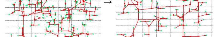
4 Flip-Flop Flop Merging Merge several 1-bit Flip-Flops into a Multi- bit Flip-Flop Flop (MBFF) Eliminate some inverters and area Reduce the # clock sinks

5 Flip-Flop Flop Merging


6 Reduction of clock sinks
7 Related Work [15] Post-placement power optimization with multi-bit flip-flops, flops ICCAD 10 The objective of [15] is to minimize the total FF Power However, our objective function is to minimize the # clock sinks and switching power of signal nets


8 Wirelength of Signal Nets Different merging solutions will affect the wirelength and switching power of signal nets differently
9 Post-Placement Placement Relocation After merging, we need to relocate these MBFFs It will affect the total switching power of signal nets
10 Outline Introduction Problem Formulation Algorithms Experimental Results Conclusions
11 Problem Formulation Inputs A preplaced design and a MBFF Library Objectives Minimize the # sinks in clock network Minimize the switching power of signal nets α i is the switching rate of signal nets
12 Constraints Guarantee there is no timing violation Feasible region of FFs Control the placement density Maintain the quality of legalization Consider routing congestion


13 Feasible Region of a FF Slack = Maximum allowed delay - D AB Slack A = Slack B = Slack / 2


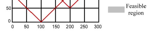
14 Feasible Region of a FF (cont.) P K Q
15 Outline Introduction Problem Formulation Algorithms Experimental Results Conclusions

16 Intersection Graph Get the feasible regions of all FFs Th i t ti f f ibl i b The intersection of feasible regions can be represented by an intersection graph


17 Design Flow
18 Find all the Maximal Cliques Finding all the maximal cliques is NPC in general graph However, it can be solved in polynomial time in the rectangle intersection graph Solve by the sweep line algorithm
19 MBFF Extraction We want to extract the MBFFs by clique partitioning Clique partitioning is a NP-Hard problem Different extraction strategies will affect The number of clock sinks The wirelength of signal nets
20 MBFF Extraction (cont.) Cost of creating MBFF β D(β ): the merging possibility of FFs in β B(β ): the # bits of β Switching gpower of signal nets connected to β α i is the switching rate of signal nets


 <")

 FF6 already")

21 Example of Extraction Algorithm Assume we have 1/2/4-bit MBFF in library There are two maximal cliques c 1 = {1,2,3,6,7}, c 2 = {4,5,6} Random sampling 1, 2 or 4 of FFs from c 1, c 2 β 1 = {1,2,3,6}, β 2 = {4,6} cost(β 1 ) < cost(β 2 ) => select β 1 Re-sampling β 1 = {7} from c 1 cost(β 2 ) < cost(β 1 ) FF6 already covered Re-sampling β 2 = {4, 5} from c 2 Final Extraction {β 1, β 2, β 1 }


22 MBFF Relocation For a MBFF β, we want to minimize the switching power of its signal nets α i is the switching rate of signal nets We can formulate it as a weighted median problem
23 MBFF Relocation (cont.) The weight of P1~P5 are 2:1:1:3:1
 Because of bin density")

24 MBFF Relocation (cont.) Because of bin density constraints, some MBFFs cannot be placed in preferred region
25 Outline Introduction Problem Formulation Algorithms Experimental Results Conclusions
26 Experimental Setup Implemented in C++ Work on Linux with 2.13GHz CPU We have 9 test cases r1~r5 r5 from [22] Exact Zero-Skew t0~t3 from 2010 CAD contest of Taiwan Random generate switching rates 5%~15%
27 Experimental Results Reduction of clock sinks and wirelength of clock tree


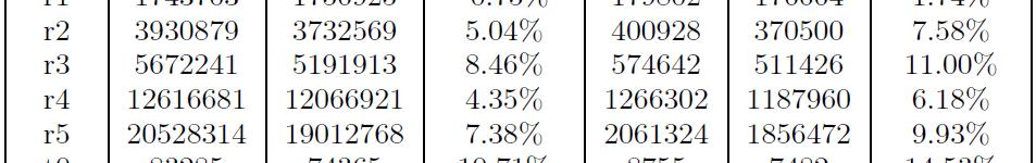


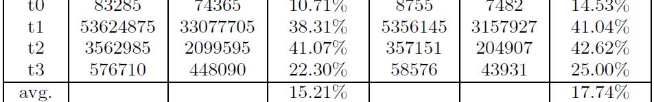


28 Experimental Results (cont.) Reduction of wirelength and estimated switching power of nets connected to FFs
29 Comparison with [15] Our algorithm can be modified to target the objectives of [15]
30 Conclusions We present a power-driven flip-flop merging and relocation approach to reduce the switching power consumption of the entire circuit
31 Q&A Thanks for your attention
Novel Pulsed-Latch Replacement Based on Time Borrowing and Spiral Clustering
 Novel Pulsed-Latch Replacement Based on Time Borrowing and Spiral Clustering NCTU CHIH-LONG CHANG IRIS HUI-RU JIANG YU-MING YANG EVAN YU-WEN TSAI AKI SHENG-HUA CHEN IRIS Lab National Chiao Tung University
Flip-flop Clustering by Weighted K-means Algorithm
 Flip-flop Clustering by Weighted K-means Algorithm Gang Wu, Yue Xu, Dean Wu, Manoj Ragupathy, Yu-yen Mo and Chris Chu Department of Electrical and Computer Engineering, Iowa State University, IA, United
COPY RIGHT. To Secure Your Paper As Per UGC Guidelines We Are Providing A Electronic Bar Code
 COPY RIGHT 2018IJIEMR.Personal use of this material is permitted. Permission from IJIEMR must be obtained for all other uses, in any current or future media, including reprinting/republishing this material
A Survey on Post-Placement Techniques of Multibit Flip-Flops
 International Journal of Engineering Research and Development e-issn: 2278-067X, p-issn: 2278-800X, www.ijerd.com Volume 10, Issue 3 (March 2014), PP.11-18 A Survey on Post-Placement Techniques of Multibit
Post-Routing Layer Assignment for Double Patterning
 Post-Routing Layer Assignment for Double Patterning Jian Sun 1, Yinghai Lu 2, Hai Zhou 1,2 and Xuan Zeng 1 1 Micro-Electronics Dept. Fudan University, China 2 Electrical Engineering and Computer Science
Clock Tree Power Optimization of Three Dimensional VLSI System with Network
 Clock Tree Power Optimization of Three Dimensional VLSI System with Network M.Saranya 1, S.Mahalakshmi 2, P.Saranya Devi 3 PG Student, Dept. of ECE, Syed Ammal Engineering College, Ramanathapuram, Tamilnadu,
Australian Journal of Basic and Applied Sciences. Design of SRAM using Multibit Flipflop with Clock Gating Technique
 ISSN:1991-8178 Australian Journal of Basic and Applied Sciences Journal home page: www.ajbasweb.com Design of SRAM using Multibit Flipflop with Clock Gating Technique 1 Divya R. and 2 Hemalatha K.L. 1
DUE to the popularity of portable electronic products,
 64 IEEE TRANSACTIONS ON VERY LARGE SCALE INTEGRATION (VLSI) SYSTEMS, VOL. 1, NO. 4, APRIL 013 Effective and Efficient Approach for Power Reduction by Using Multi-Bit Flip-Flops Ya-Ting Shyu, Jai-Ming Lin,
Power Reduction Approach by using Multi-Bit Flip-Flops
 International Journal of Emerging Engineering Research and Technology Volume 2, Issue 4, July 2014, PP 60-77 ISSN 2349-4395 (Print) & ISSN 2349-4409 (Online) Power Reduction Approach by using Multi-Bit
Reduction of Clock Power in Sequential Circuits Using Multi-Bit Flip-Flops
 Reduction of Clock Power in Sequential Circuits Using Multi-Bit Flip-Flops A.Abinaya *1 and V.Priya #2 * M.E VLSI Design, ECE Dept, M.Kumarasamy College of Engineering, Karur, Tamilnadu, India # M.E VLSI
Latch-Based Performance Optimization for FPGAs. Xiao Teng
 Latch-Based Performance Optimization for FPGAs by Xiao Teng A thesis submitted in conformity with the requirements for the degree of Master of Applied Science Graduate Department of ECE University of Toronto
K.T. Tim Cheng 07_dft, v Testability
 K.T. Tim Cheng 07_dft, v1.0 1 Testability Is concept that deals with costs associated with testing. Increase testability of a circuit Some test cost is being reduced Test application time Test generation
Improved Flop Tray-Based Design Implementation for Power Reduction
 Improved Flop Tray-Based Design Implementation for Power Reduction Andrew B. Kahng, Jiajia Li and Lutong Wang CSE and ECE Departments, UC San Diego, La Jolla, CA, USA {abk, jil150, luw002}@ucsd.edu ABSTRACT
ECE 301 Digital Electronics
 ECE 301 Digital Electronics Derivation of Flip-Flop Input Equations and State Assignment (Lecture #24) The slides included herein were taken from the materials accompanying Fundamentals of Logic Design,
AN OPTIMIZED IMPLEMENTATION OF MULTI- BIT FLIP-FLOP USING VERILOG
 AN OPTIMIZED IMPLEMENTATION OF MULTI- BIT FLIP-FLOP USING VERILOG 1 V.GOUTHAM KUMAR, Pg Scholar In Vlsi, 2 A.M.GUNA SEKHAR, M.Tech, Associate. Professor, ECE Department, 1 gouthamkumar.vakkala@gmail.com,
Interconnect Planning with Local Area Constrained Retiming
 Interconnect Planning with Local Area Constrained Retiming Ruibing Lu and Cheng-Kok Koh School of Electrical and Computer Engineering Purdue University,West Lafayette, IN, 47907, USA {lur, chengkok}@ecn.purdue.edu
A Greedy Heuristic Algorithm for Flip-Flop Replacement Power Reduction in Digital Integrated Circuits
 A Greedy Heuristic Algorithm for Flip-Flop Replacement Power Reduction in Digital Integrated Circuits C.N.Kalaivani 1, Ayswarya J.J 2 Assistant Professor, Dept. of ECE, Dhaanish Ahmed College of Engineering,
Prototyping an ASIC with FPGAs. By Rafey Mahmud, FAE at Synplicity.
 Prototyping an ASIC with FPGAs By Rafey Mahmud, FAE at Synplicity. With increased capacity of FPGAs and readily available off-the-shelf prototyping boards sporting multiple FPGAs, it has become feasible
Asynchronous IC Interconnect Network Design and Implementation Using a Standard ASIC Flow
 Asynchronous IC Interconnect Network Design and Implementation Using a Standard ASIC Flow Bradley R. Quinton*, Mark R. Greenstreet, Steven J.E. Wilton*, *Dept. of Electrical and Computer Engineering, Dept.
QDR SRAM DESIGN USING MULTI-BIT FLIP-FLOP M.Ananthi, C.Sathish Kumar 1. INTRODUCTION In memory devices the most
 International Journal of Avance Research in Electronics an Communication Engineering (IJARECE) ABSTRACT: QDR SRAM DESIGN USING MULTI-BIT FLIP-FLOP M.Ananthi, C.Sathish Kumar 1. INTRODUCTION In memor evices
REDUCING DYNAMIC POWER BY PULSED LATCH AND MULTIPLE PULSE GENERATOR IN CLOCKTREE
 Available Online at www.ijcsmc.com International Journal of Computer Science and Mobile Computing A Monthly Journal of Computer Science and Information Technology IJCSMC, Vol. 3, Issue. 5, May 2014, pg.210
Iterative Deletion Routing Algorithm
 Iterative Deletion Routing Algorithm Perform routing based on the following placement Two nets: n 1 = {b,c,g,h,i,k}, n 2 = {a,d,e,f,j} Cell/feed-through width = 2, height = 3 Shift cells to the right,
University College of Engineering, JNTUK, Kakinada, India Member of Technical Staff, Seerakademi, Hyderabad
 Power Analysis of Sequential Circuits Using Multi- Bit Flip Flops Yarramsetti Ramya Lakshmi 1, Dr. I. Santi Prabha 2, R.Niranjan 3 1 M.Tech, 2 Professor, Dept. of E.C.E. University College of Engineering,
Chapter 5 Synchronous Sequential Logic
 Chapter 5 Synchronous Sequential Logic Chih-Tsun Huang ( 黃稚存 ) http://nthucad.cs.nthu.edu.tw/~cthuang/ Department of Computer Science National Tsing Hua University Outline Introduction Storage Elements:
More design examples, state assignment and reduction. Page 1
 More design examples, state assignment and reduction Page 1 Serial Parity Checker We have only 2 states (S 0, S 1 ): correspond to an even and odd number of 1 s received so far. x Clock D FF Q Z = 1 whenever
Slack Redistribution for Graceful Degradation Under Voltage Overscaling
 Slack Redistribution for Graceful Degradation Under Voltage Overscaling Andrew B. Kahng, Seokhyeong Kang, Rakesh Kumar and John Sartori VLSI CAD LABORATORY, UCSD PASSAT GROUP, UIUC UCSD VLSI CAD Laboratory
DEPARTMENT OF ELECTRICAL &ELECTRONICS ENGINEERING DIGITAL DESIGN
 DEPARTMENT OF ELECTRICAL &ELECTRONICS ENGINEERING DIGITAL DESIGN Assoc. Prof. Dr. Burak Kelleci Spring 2018 OUTLINE Synchronous Logic Circuits Latch Flip-Flop Timing Counters Shift Register Synchronous
Low Voltage Clocking Methodologies for Nanoscale ICs. A Dissertation Presented. Weicheng Liu. The Graduate School. in Partial Fulfillment of the
 Low Voltage Clocking Methodologies for Nanoscale ICs A Dissertation Presented by Weicheng Liu to The Graduate School in Partial Fulfillment of the Requirements for the Degree of Doctor of Philosophy in
Retiming Sequential Circuits for Low Power
 Retiming Sequential Circuits for Low Power José Monteiro, Srinivas Devadas Department of EECS MIT, Cambridge, MA Abhijit Ghosh Mitsubishi Electric Research Laboratories Sunnyvale, CA Abstract Switching
Gated Driver Tree Based Power Optimized Multi-Bit Flip-Flops
 International Journal of Emerging Engineering Research and Technology Volume 2, Issue 4, July 2014, PP 250-254 ISSN 2349-4395 (Print) & ISSN 2349-4409 (Online) Gated Driver Tree Based Power Optimized Multi-Bit
VirtualSync: Timing Optimization by Synchronizing Logic Waves with Sequential and Combinational Components as Delay Units
 VirtualSync: Timing Optimization by Synchronizing Logic Waves with Sequential and Combinational Components as Delay Units Grace Li Zhang 1, Bing Li 1, Masanori Hashimoto 2 and Ulf Schlichtmann 1 1 Chair
Power-Optimal Pipelining in Deep Submicron Technology
 ISLPED 2004 8/10/2004 -Optimal Pipelining in Deep Submicron Technology Seongmoo Heo and Krste Asanovi Computer Architecture Group, MIT CSAIL Traditional Pipelining Goal: Maximum performance Vdd Clk-Q Setup
Controlling Peak Power During Scan Testing
 Controlling Peak Power During Scan Testing Ranganathan Sankaralingam and Nur A. Touba Computer Engineering Research Center Department of Electrical and Computer Engineering University of Texas, Austin,
Chapter 12. Synchronous Circuits. Contents
 Chapter 12 Synchronous Circuits Contents 12.1 Syntactic definition........................ 149 12.2 Timing analysis: the canonic form............... 151 12.2.1 Canonic form of a synchronous circuit..............
Instructions. Final Exam CPSC/ELEN 680 December 12, Name: UIN:
 Final Exam CPSC/ELEN 680 December 12, 2005 Name: UIN: Instructions This exam is closed book. Provide brief but complete answers to the following questions in the space provided, using figures as necessary.
Design for Testability
 TDTS 01 Lecture 9 Design for Testability Zebo Peng Embedded Systems Laboratory IDA, Linköping University Lecture 9 The test problems Fault modeling Design for testability techniques Zebo Peng, IDA, LiTH
Testability: Lecture 23 Design for Testability (DFT) Slide 1 of 43
 Slide 1 of 43") Testability: Lecture 23 Design for Testability (DFT) Shaahin hi Hessabi Department of Computer Engineering Sharif University of Technology Adapted, with modifications, from lecture notes prepared p by
Testability: Lecture 23 Design for Testability (DFT) Shaahin hi Hessabi Department of Computer Engineering Sharif University of Technology Adapted, with modifications, from lecture notes prepared p by
Low Power VLSI Circuits and Systems Prof. Ajit Pal Department of Computer Science and Engineering Indian Institute of Technology, Kharagpur
 Low Power VLSI Circuits and Systems Prof. Ajit Pal Department of Computer Science and Engineering Indian Institute of Technology, Kharagpur Lecture No. # 29 Minimizing Switched Capacitance-III. (Refer
Timing with Virtual Signal Synchronization for Circuit Performance and Netlist Security
 Timing with Virtual Signal Synchronization for Circuit Performance and Netlist Security Grace Li Zhang, Bing Li, Ulf Schlichtmann Chair of Electronic Design Automation Technical University of Munich (TUM)
International Journal of Emerging Technologies in Computational and Applied Sciences (IJETCAS)
") International Association of Scientific Innovation and Research (IASIR) (An Association Unifying the Sciences, Engineering, and Applied Research) International Journal of Emerging Technologies in Computational
International Association of Scientific Innovation and Research (IASIR) (An Association Unifying the Sciences, Engineering, and Applied Research) International Journal of Emerging Technologies in Computational
EECS 427 Discussion 1
 EECS 427 Discussion 1 Tuesday, September 9, 2008 1 1 Administrative Stuff CAD1 due yesterday Homework 1 due Thursday, beginning of lecture Homework 2 due week from today Sept. 16 Due at beginning of Tuesday
11. Sequential Elements
 11. Sequential Elements Jacob Abraham Department of Electrical and Computer Engineering The University of Texas at Austin VLSI Design Fall 2017 October 11, 2017 ECE Department, University of Texas at Austin
More on Flip-Flops Digital Design and Computer Architecture: ARM Edition 2015 Chapter 3 <98> 98
 More on Flip-Flops Digital Design and Computer Architecture: ARM Edition 2015 Chapter 3 98 Review: Bit Storage SR latch S (set) Q R (reset) Level-sensitive SR latch S S1 C R R1 Q D C S R D latch Q
Achieving Faster Time to Tapeout with In-Design, Signoff-Quality Metal Fill
 White Paper Achieving Faster Time to Tapeout with In-Design, Signoff-Quality Metal Fill May 2009 Author David Pemberton- Smith Implementation Group, Synopsys, Inc. Executive Summary Many semiconductor
EET2411 DIGITAL ELECTRONICS
 5-8 Clocked D Flip-FlopFlop One data input. The output changes to the value of the input at either the positive going or negative going clock trigger. May be implemented with a J-K FF by tying the J input
Sequencing. Lan-Da Van ( 范倫達 ), Ph. D. Department of Computer Science National Chiao Tung University Taiwan, R.O.C. Fall,
, Ph. D. Department of Computer Science National Chiao Tung University Taiwan, R.O.C. Fall,") Sequencing ( 范倫達 ), Ph. D. Department of Computer Science National Chiao Tung University Taiwan, R.O.C. Fall, 2013 ldvan@cs.nctu.edu.tw http://www.cs.nctu.edu.tw/~ldvan/ Outlines Introduction Sequencing
Sequencing ( 范倫達 ), Ph. D. Department of Computer Science National Chiao Tung University Taiwan, R.O.C. Fall, 2013 ldvan@cs.nctu.edu.tw http://www.cs.nctu.edu.tw/~ldvan/ Outlines Introduction Sequencing
Synthesis of Reversible Sequential Elements
 Synthesis of Reversible Sequential Elements Speaker:Kuang-Jung Chang Author: Min-Lun Chuang Chun-Yao Wang Dept. of Computer Science National Tsing Hua University, Taiwan Introduction Outline Background
Clock-Aware FPGA Placement Contest
 Clock-Aware FPGA Placement Contest Stephen Yang, Chandra Mulpuri, Sainath Reddy, Meghraj Kalase, Srinivasan Dasasathyan, Mehrdad E. Dehkordi, Marvin Tom, Rajat Aggarwal Xilinx Inc. 2100 Logic Drive San
Design Project: Designing a Viterbi Decoder (PART I)
") Digital Integrated Circuits A Design Perspective 2/e Jan M. Rabaey, Anantha Chandrakasan, Borivoje Nikolić Chapters 6 and 11 Design Project: Designing a Viterbi Decoder (PART I) 1. Designing a Viterbi
Digital Integrated Circuits A Design Perspective 2/e Jan M. Rabaey, Anantha Chandrakasan, Borivoje Nikolić Chapters 6 and 11 Design Project: Designing a Viterbi Decoder (PART I) 1. Designing a Viterbi
EXPLOITING LEVEL SENSITIVE LATCHES FOR WIRE PIPELINING. A Thesis VIKRAM SETH
 EXPLOITING LEVEL SENSITIVE LATCHES FOR WIRE PIPELINING A Thesis by VIKRAM SETH Submitted to the Office of Graduate Studies of Texas A&M University in partial fulfillment of the requirements for the degree
Lecture 23 Design for Testability (DFT): Full-Scan
: Full-Scan") Lecture 23 Design for Testability (DFT): Full-Scan (Lecture 19alt in the Alternative Sequence) Definition Ad-hoc methods Scan design Design rules Scan register Scan flip-flops Scan test sequences Overheads
Lecture 23 Design for Testability (DFT): Full-Scan (Lecture 19alt in the Alternative Sequence) Definition Ad-hoc methods Scan design Design rules Scan register Scan flip-flops Scan test sequences Overheads
EL302 DIGITAL INTEGRATED CIRCUITS LAB #3 CMOS EDGE TRIGGERED D FLIP-FLOP. Due İLKER KALYONCU, 10043
 EL302 DIGITAL INTEGRATED CIRCUITS LAB #3 CMOS EDGE TRIGGERED D FLIP-FLOP Due 16.05. İLKER KALYONCU, 10043 1. INTRODUCTION: In this project we are going to design a CMOS positive edge triggered master-slave
Digital Logic Design Sequential Circuits. Dr. Basem ElHalawany
 Digital Logic Design Sequential Circuits Dr. Basem ElHalawany Combinational vs Sequential inputs X Combinational Circuits outputs Z A combinational circuit: At any time, outputs depends only on inputs
Final Exam review: chapter 4 and 5. Supplement 3 and 4
 Final Exam review: chapter 4 and 5. Supplement 3 and 4 1. A new type of synchronous flip-flop has the following characteristic table. Find the corresponding excitation table with don t cares used as much
Unit 11. Latches and Flip-Flops
 Unit 11 Latches and Flip-Flops 1 Combinational Circuits A combinational circuit consists of logic gates whose outputs, at any time, are determined by combining the values of the inputs. For n input variables,
Logic and Computer Design Fundamentals. Chapter 7. Registers and Counters
 Logic and Computer Design Fundamentals Chapter 7 Registers and Counters Registers Register a collection of binary storage elements In theory, a register is sequential logic which can be defined by a state
Software Engineering 2DA4. Slides 3: Optimized Implementation of Logic Functions
 Software Engineering 2DA4 Slides 3: Optimized Implementation of Logic Functions Dr. Ryan Leduc Department of Computing and Software McMaster University Material based on S. Brown and Z. Vranesic, Fundamentals
Combining Dual-Supply, Dual-Threshold and Transistor Sizing for Power Reduction
 Combining Dual-Supply, Dual-Threshold and Transistor Sizing for Reduction Stephanie Augsburger 1, Borivoje Nikolić 2 1 Intel Corporation, Enterprise Processors Division, Santa Clara, CA, USA. 2 Department
Impact of Test Point Insertion on Silicon Area and Timing during Layout
 Impact of Test Point Insertion on Silicon Area and Timing during Layout Harald Vranken Ferry Syafei Sapei 2 Hans-Joachim Wunderlich 2 Philips Research Laboratories IC Design Digital Design & Test Prof.
TKK S ASIC-PIIRIEN SUUNNITTELU
 Design TKK S-88.134 ASIC-PIIRIEN SUUNNITTELU Design Flow 3.2.2005 RTL Design 10.2.2005 Implementation 7.4.2005 Contents 1. Terminology 2. RTL to Parts flow 3. Logic synthesis 4. Static Timing Analysis
High Performance Low Swing Clock Tree Synthesis with Custom D Flip-Flop Design
 2014 IEEE Computer Society Annual Symposium on VLSI High Performance Low Swing Clock Tree Synthesis with Custom D Flip-Flop Design Can Sitik, Leo Filippini Electrical and Computer Engineering Drexel University
Figure.1 Clock signal II. SYSTEM ANALYSIS
 International Journal of Advances in Engineering, 2015, 1(4), 518-522 ISSN: 2394-9260 (printed version); ISSN: 2394-9279 (online version); url:http://www.ijae.in RESEARCH ARTICLE Multi bit Flip-Flop Grouping
CS/EE 6710 Digital VLSI Design CAD Assignment #3 Due Thursday September 21 st, 5:00pm
 CS/EE 6710 Digital VLSI Design CAD Assignment #3 Due Thursday September 21 st, 5:00pm Overview: In this assignment you will design a register cell. This cell should be a single-bit edge-triggered D-type
Final Exam CPSC/ECEN 680 May 2, Name: UIN:
 Final Exam CPSC/ECEN 680 May 2, 2008 Name: UIN: Instructions This exam is closed book. Provide brief but complete answers to the following questions in the space provided, using figures as necessary. Show
Flip-Flops. Because of this the state of the latch may keep changing in circuits with feedback as long as the clock pulse remains active.
 Flip-Flops Objectives The objectives of this lesson are to study: 1. Latches versus Flip-Flops 2. Master-Slave Flip-Flops 3. Timing Analysis of Master-Slave Flip-Flops 4. Different Types of Master-Slave
More Digital Circuits
 More Digital Circuits 1 Signals and Waveforms: Showing Time & Grouping 2 Signals and Waveforms: Circuit Delay 2 3 4 5 3 10 0 1 5 13 4 6 3 Sample Debugging Waveform 4 Type of Circuits Synchronous Digital
CSE 352 Laboratory Assignment 3
 CSE 352 Laboratory Assignment 3 Introduction to Registers The objective of this lab is to introduce you to edge-trigged D-type flip-flops as well as linear feedback shift registers. Chapter 3 of the Harris&Harris
Fundamentals of Computer Systems
 Fundamentals of omputer Systems Sequential Logic Martha A. Kim olumbia University Spring 2016 1/1 2/1 Bistable Elements Equivalent circuits; right is more traditional. Two stable states: 0 1 1 0 3/1 S
A Technique to Reduce Peak Current and Average Power Dissipation in Scan Designs by Limited Capture
 A Technique to Reduce Peak Current and Average Power Dissipation in Scan Designs by Limited Capture Seongmoon Wang Wenlong Wei NEC Labs., America, Princeton, NJ swang,wwei @nec-labs.com Abstract In this
Peak Dynamic Power Estimation of FPGA-mapped Digital Designs
 Peak Dynamic Power Estimation of FPGA-mapped Digital Designs Abstract The Peak Dynamic Power Estimation (P DP E) problem involves finding input vector pairs that cause maximum power dissipation (maximum
ASYNCHRONOUS COUNTER CIRCUITS
 ASYNCHRONOUS COUNTER CIRCUITS Asynchronous counters do not have a common clock that controls all the Hipflop stages. The control clock is input into the first stage, or the LSB stage of the counter. The
ECE 715 System on Chip Design and Test. Lecture 22
 ECE 75 System on Chip Design and Test Lecture 22 Response Compaction Severe amounts of data in CUT response to LFSR patterns example: Generate 5 million random patterns CUT has 2 outputs Leads to: 5 million
Introduction to Sequential Circuits
 Introduction to Sequential Circuits COE 202 Digital Logic Design Dr. Muhamed Mudawar King Fahd University of Petroleum and Minerals Presentation Outline Introduction to Sequential Circuits Synchronous
Scan Chain Design for Power Minimization During Scan Testing Under Routing Constraint.
 Efficient Scan Chain Design for Power Minimization During Scan Testing Under Routing Constraint Yannick Bonhomme, Patrick Girard, L. Guiller, Christian Landrault, Serge Pravossoudovitch To cite this version:
Sequential Circuit Design: Principle
 Sequential Circuit Design: Principle modified by L.Aamodt 1 Outline 1. 2. 3. 4. 5. 6. 7. 8. Overview on sequential circuits Synchronous circuits Danger of synthesizing asynchronous circuit Inference of
VLSI Design: 3) Explain the various MOSFET Capacitances & their significance. 4) Draw a CMOS Inverter. Explain its transfer characteristics
 Explain the various MOSFET Capacitances & their significance. 4) Draw a CMOS Inverter. Explain its transfer characteristics") 1) Explain why & how a MOSFET works VLSI Design: 2) Draw Vds-Ids curve for a MOSFET. Now, show how this curve changes (a) with increasing Vgs (b) with increasing transistor width (c) considering Channel
1) Explain why & how a MOSFET works VLSI Design: 2) Draw Vds-Ids curve for a MOSFET. Now, show how this curve changes (a) with increasing Vgs (b) with increasing transistor width (c) considering Channel
Why FPGAs? FPGA Overview. Why FPGAs?
 Transistor-level Logic Circuits Positive Level-sensitive EECS150 - Digital Design Lecture 3 - Field Programmable Gate Arrays (FPGAs) January 28, 2003 John Wawrzynek Transistor Level clk clk clk Positive
EEC 118 Lecture #9: Sequential Logic. Rajeevan Amirtharajah University of California, Davis Jeff Parkhurst Intel Corporation
 EEC 118 Lecture #9: Sequential Logic Rajeevan Amirtharajah University of California, Davis Jeff Parkhurst Intel Corporation Outline Review: Static CMOS Logic Finish Static CMOS transient analysis Sequential
Minimizing Leakage of Sequential Circuits through Flip-Flop Skewing and Technology Mapping
 JOURNAL OF SEMICONDUCTOR TECHNOLOGY AND SCIENCE, VOL.7, NO.4, DECEMER, 2007 215 Minimizing Leakage of Sequential Circuits through Flip-Flop Skewing and Technology Mapping Sewan Heo and Youngsoo Shin Abstract
A Proposal for Routing-Based Timing-Driven Scan Chain Ordering
 A Proposal for Routing-Based Timing-Driven Scan Chain Ordering Puneet Gupta, Andrew B. Kahng and Stefanus Mantik Department of Electrical and Computer Engineering, UC San Diego, La Jolla, CA, USA Department
A Critical-Path-Aware Partial Gating Approach for Test Power Reduction
 A Critical-Path-Aware Partial Gating Approach for Test Power Reduction MOHAMMED ELSHOUKRY University of Maryland MOHAMMAD TEHRANIPOOR University of Connecticut and C. P. RAVIKUMAR Texas Instruments India
VLSI Design Digital Systems and VLSI
 VLSI Design Digital Systems and VLSI Somayyeh Koohi Department of Computer Engineering Adapted with modifications from lecture notes prepared by author 1 Overview Why VLSI? IC Manufacturing CMOS Technology
Design for Testability Part II
 Design for Testability Part II 1 Partial-Scan Definition A subset of flip-flops is scanned. Objectives: Minimize area overhead and scan sequence length, yet achieve required fault coverage. Exclude selected
Fundamentals of Computer Systems
 Fundamentals of Computer Systems Sequential Logic Stephen A. Edwards Columbia University Fall 2012 State-Holding Elements Bistable Elements Equivalent circuits; right is more traditional. Two stable states:
IN DIGITAL transmission systems, there are always scramblers
 558 IEEE TRANSACTIONS ON CIRCUITS AND SYSTEMS II: EXPRESS BRIEFS, VOL. 53, NO. 7, JULY 2006 Parallel Scrambler for High-Speed Applications Chih-Hsien Lin, Chih-Ning Chen, You-Jiun Wang, Ju-Yuan Hsiao,
Exploring Architecture Parameters for Dual-Output LUT based FPGAs
 Exploring Architecture Parameters for Dual-Output LUT based FPGAs Zhenghong Jiang, Colin Yu Lin, Liqun Yang, Fei Wang and Haigang Yang System on Programmable Chip Research Department, Institute of Electronics,
ISPD 2017 Contest Clock-Aware FPGA Placement
 ISPD 2017 Contest Clock-Aware FPGA Placement Stephen Yang, Chandra Mulpuri, Sainath Reddy, Meghraj Kalase, Srinivasan Dasasathyan, Mehrdad E. Dehkordi, Marvin Tom, Rajat Aggarwal Acknowledgement Xilinx
Power Distribution and Clock Design
 Lecture 3 Power Distribution and Clock Design R. Saleh Dept. of ECE University of British Columbia res@ece.ubc.ca 1 Overview of Lecture Power distribution in the past was a fairly simple task Goal of power
A Modified Static Contention Free Single Phase Clocked Flip-flop Design for Low Power Applications
 JOURNAL OF SEMICONDUCTOR TECHNOLOGY AND SCIENCE, VOL.8, NO.5, OCTOBER, 08 ISSN(Print) 598-657 https://doi.org/57/jsts.08.8.5.640 ISSN(Online) -4866 A Modified Static Contention Free Single Phase Clocked
Computer Organization & Architecture Lecture #5
 Computer Organization & Architecture Lecture #5 Shift Register A shift register is a register in which binary data can be stored and then shifted left or right when a shift signal is applied. Bits shifted
Chapter 7 Sequential Circuits
 Chapter 7 Sequential Circuits Jin-Fu Li Advanced Reliable Systems (ARES) Lab. epartment of Electrical Engineering National Central University Jungli, Taiwan Outline Latches & Registers Sequencing Timing
Introduction. Serial In - Serial Out Shift Registers (SISO)
") Introduction Shift registers are a type of sequential logic circuit, mainly for storage of digital data. They are a group of flip-flops connected in a chain so that the output from one flip-flop becomes
Introduction Shift registers are a type of sequential logic circuit, mainly for storage of digital data. They are a group of flip-flops connected in a chain so that the output from one flip-flop becomes
Power-Aware Placement
 Power-Aware Placement Yongseok Cheon, Pei-Hsin Ho, Andrew B. Kahng, Sherief Reda, Qinke Wang Advanced Technology Group, Synopsys, Inc. CSE Department, University of California at San Diego {cheon,pho}@synopsys.com,
1. What does the signal for a static-zero hazard look like?
 Sample Problems 1. What does the signal for a static-zero hazard look like? The signal will always be logic zero except when the hazard occurs which will cause it to temporarly go to logic one (i.e. glitch
Jin-Fu Li Advanced Reliable Systems (ARES) Laboratory. National Central University
 Laboratory. National Central University") Chapter 3 Basics of VLSI Testing (2) Jin-Fu Li Advanced Reliable Systems (ARES) Laboratory Department of Electrical Engineering National Central University Jhongli, Taiwan Outline Testing Process Fault
Chapter 3 Basics of VLSI Testing (2) Jin-Fu Li Advanced Reliable Systems (ARES) Laboratory Department of Electrical Engineering National Central University Jhongli, Taiwan Outline Testing Process Fault
Asynchronous (Ripple) Counters
 Counters") Circuits for counting events are frequently used in computers and other digital systems. Since a counter circuit must remember its past states, it has to possess memory. The chapter about flip-flops introduced
Circuits for counting events are frequently used in computers and other digital systems. Since a counter circuit must remember its past states, it has to possess memory. The chapter about flip-flops introduced
Pulsed-Latch ASIC Synthesis in Industrial Design Flow
 Pulsed-Latch AC Synthesis in Industrial Design Flow Sangmin Kim, Duckhwan Kim, and Youngsoo Shin Departmt of Electrical Engineering, KAIST Daejeon 35-71, Korea Abstract Flip-flop has long be used as a
Power Efficient Design of Sequential Circuits using OBSC and RTPG Integration
 Available Online at www.ijcsmc.com International Journal of Computer Science and Mobile Computing A Monthly Journal of Computer Science and Information Technology IJCSMC, Vol. 2, Issue. 9, September 2013,
The Effect of Wire Length Minimization on Yield
 The Effect of Wire Length Minimization on Yield Venkat K. R. Chiluvuri, Israel Koren and Jeffrey L. Burns' Department of Electrical and Computer Engineering University of Massachusetts, Amherst, MA 01003
EEC 116 Fall 2011 Lab #5: Pipelined 32b Adder
 EEC 116 Fall 2011 Lab #5: Pipelined 32b Adder Dept. of Electrical and Computer Engineering University of California, Davis Issued: November 2, 2011 Due: November 16, 2011, 4PM Reading: Rabaey Sections