Using down to a Single Scan Channel to Meet your Test Goals (Part 2) Richard Illman Member of Technical Staff
|
|
|
- Martin McCormick
- 5 years ago
- Views:
Transcription
 Richard Illman Member of Technical")
1 Using down to a Single Scan Channel to Meet your Test Goals (Part 2) Richard Illman Member of Technical Staff
2 Motivation - Target Market Dialog Semiconductor creates energy-efficient, highly integrated, mixed signal circuits optimised for smartphones, tablets, ULTRABOOKS and other portable devices. Implications: Low pin count devices Large volumes (10s millions to 100s millions) Price competitive 2
3 Reducing Pin Count Example Audio Design Limited digital pins available: Clock input/output 3 pins I2C interface 2 pins I2S interface 4 pins Typically limited 3 or 4 pairs scan in/out pads 3
4 Dual use of audio analogue input pads Analogue audio input pads can be as digital inputs in scan mode. Issues: Typically must be level shifted in the chip to the digital supply levels. Load board must support both analogue and digital channels for the same pad. Mixes the analogue/digital design environments. 4
5 Requirement for high X-tolerance Large amounts of non-scan elements latches Ratio 2:1 of scan to non-scan elements Register files, filter blocks etc. Tolerance to problems in sub-chains in analogue blocks Real Time Counter, PLL 5


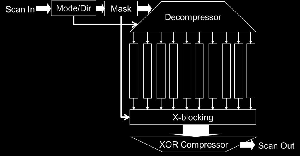
6 High X tolerance DFTMAX architecture Number of scan-in and scan-out pins Maximum internal chains
7 DFTMAX X-mask statistics in example audio design 3875 scan patterns 302 mask-only patterns 230 patterns without X-masking (~6%) 3342 patterns with X-masking Average 55 mask bits (chain length 181 bits) 7


8 High X tolerance DFTMAX with Serialiser 8


9 Serialiser Shift Clock Ratios External Shift Internal Shift 9
10 Compression Goldilocks type problem? DFTMAX too many pins DFTMAX Serialiser too slow, too much data DFTMAX Ultra baby bear solution - just right? 10

11 DFTMAX Ultra Architecture 11

12 DFTMAX Ultra shift External Shift Internal Shift 12
13 Change to the Design Compiler Synthesis Flow set_dft_configuration -scan_compression enable set_scan_compression_configuration \ -xtolerance high \ -chain_count 32 -inputs 4 -outputs 4 \ -min_power true report_scan_compression_configuration set_dft_configuration -streaming_compression enable set_streaming_compression_configuration \ -chain_count 120 -inputs 4 -outputs 4 report_streaming_compression_configuration 13
14 DFTMax Ultra overhead (Design has 6,300 scan flops and 3,500 non-scan latches) Architecture #si/so pins Internal Chains Latches added DFF added Seq. element overhead* Fault list overhead** DFTMAX % DFTMAX Ultra % 1.06% DFTMAX Ultra % 2.05% DFTMAX Ultra % 3.31% DFTMAX Ultra % 4.25% DFTMAX serializer % 0.29% DFTMAX Ultra % 0.90% 14
15 Test Coverage Single SI/SO results Serializer (one pair scan-in/scan-out) Factor 2.8 Reduction Ultra 32 DFTMAX Serializer Cycles With Minimum Detect ATPG the reduction is
16 Test Coverage 4 SI/SO test case 100 Standard ATPG DFTMAX Ultra Ultra Ultra Ultra Cycles 16

17 DFTMAX Ultra Budgeter 17

18 DFTMAX Ultra Budgeter `And thirdly, the Pirate Code DFTMAX Ultra Budgeter is more what you'd call "guidelines" than actual rules.` Captain Barbossa, Pirates of the Caribbean 18
19 Effective Chain Lengths 200 Effective Chain Length Internal Chain Internal Plus Compression Logic DFTMAX 4_4_32 Ultra 4_4_40 Ultra 4_4_80 Ultra 4_4_120 Ultra 4_4_160 19
20 Test Coverage 4 SI/SO test case 100 Standard ATPG DFTMAX Ultra Ultra Ultra Ultra Cycles 20
21 Information encoded in each pattern DFTMAX Mask data for the unload of the previous pattern Decompressor mode for the current pattern Data is encoded on a cycle basis through the whole pattern DFTMAX Ultra Mask data and compressor direction for the current pattern Decompressor mode and direction for the next pattern Data is encoded in separate dedicated bits High X-tolerance DFTMAX patterns which utilise X-masking cannot be individually manipulated, DFTMAX Ultra patterns can. 21
22 ATPG Minimum Detect set_atpg -basic_min_detects_per_pattern { d d } \ -fast_min_detects_per_pattern { d d } parameters minimum number of fault detects limit on consecutive rejected patterns set i 8192 while { $i > 2 } { set i [expr $i/2] ; set_atpg -fast_min_detect [list $i 20]; run_atpg fast -auto } 22
23 DFTMAX Ultra Pattern Reordering Command Post ATPG (Beta status) reorder_patterns coverage \ sort partial \ group_size <d> \ -number_of_patterns <d> reorder_patterns coverage sort full \ first_pattern <d> \ -last_pattern <d> 23
24 Pattern reordering fault simulation based Extracting fault detections for each pattern set limit [expr [sizeof_collection [get_patterns -all ]] -1 ] for { set i 0 } { $i < $limit } { incr i } { run_fault_sim first $i last $i } Very slow and inefficient run_fault_sim -detected_pattern_storage write_patterns filename -all Fault list contains the first pattern where the fault is detected Not available with multi-processor 24
25 DFTMAX Ultra Pattern Reordering Command User defined list reorder_patterns -remove { } -insert { X X X X X X X X } The first list is the patterns to be removed. The corresponding item in the second list is the position it is to be placed. If the item in the second list is X the pattern is deleted. Over 50,000 patterns successfully reordered with a single command. Legacy patterns reordered with: write_patterns filename -reorder file 25
26 Test Coverage DFTMAX Ultra with minimum detect 20 rejected pattern limit 100 Minimum Detect ATPG DFTMAX Ultra Ultra Min Detect Ultra Ultra Min Detect Ultra Ultra Min Detect Cycles 26
27 Test Coverage Reordering of minimum detect patterns 100 Reordering of min_detect patterns DFTMAX Ultra Ultra Reorder 1 Ultra Reorder Cycles 27
28 Test Coverage Legacy design reordering Basic, single load sequential, multi load sequential 100 Pattern Reordering - after min_detect ATPG ATPG Reorder 1 Reorder 2 Reorder Patterns 28
29 Coverage Regeneration of Patterns 100 Regeneration Min Detect ATPG Reorder & Truncate Rerun ATPG Reorder Patterns 29
30 Reordered Pattern Position Pattern Reordering 8000 Pattern Mobility During Reordering Basic Fast Sequential Original Pattern Position 30
31 Key Advantages of DFTMAX Ultra Easy transition of the synthesis/atpg flow Dramatically improved results for the single scan in/out implementation. Higher compression achieved when pin counts are limited (or achieve the same compression with reduced pin access on the ATE). More compact pattern sets can be generated minimum detect and pattern reordering available even with High X tolerance 31
32 The power to be...
Scan. This is a sample of the first 15 pages of the Scan chapter.
 Scan This is a sample of the first 15 pages of the Scan chapter. Note: The book is NOT Pinted in color. Objectives: This section provides: An overview of Scan An introduction to Test Sequences and Test
Using on-chip Test Pattern Compression for Full Scan SoC Designs
 Using on-chip Test Pattern Compression for Full Scan SoC Designs Helmut Lang Senior Staff Engineer Jens Pfeiffer CAD Engineer Jeff Maguire Principal Staff Engineer Motorola SPS, System-on-a-Chip Design
VirtualScan TM An Application Story
 Test Data Compaction Tool from SynTest TM VirtualScan TM An Application Story January 29, 2004 Hiroshi Furukawa SoC No. 3 Group, SoC Development Division 1 Agenda Current Problems What is VirtualScan?
for Digital IC's Design-for-Test and Embedded Core Systems Alfred L. Crouch Prentice Hall PTR Upper Saddle River, NJ
 Design-for-Test for Digital IC's and Embedded Core Systems Alfred L. Crouch Prentice Hall PTR Upper Saddle River, NJ 07458 www.phptr.com ISBN D-13-DflMfla7-l : Ml H Contents Preface Acknowledgments Introduction
VLSI System Testing. BIST Motivation
 ECE 538 VLSI System Testing Krish Chakrabarty Built-In Self-Test (BIST): ECE 538 Krish Chakrabarty BIST Motivation Useful for field test and diagnosis (less expensive than a local automatic test equipment)
Lecture 23 Design for Testability (DFT): Full-Scan (chapter14)
: Full-Scan (chapter14)") Lecture 23 Design for Testability (DFT): Full-Scan (chapter14) Definition Ad-hoc methods Scan design Design rules Scan register Scan flip-flops Scan test sequences Overheads Scan design system Summary
Lecture 23 Design for Testability (DFT): Full-Scan (chapter14) Definition Ad-hoc methods Scan design Design rules Scan register Scan flip-flops Scan test sequences Overheads Scan design system Summary
Low Power Illinois Scan Architecture for Simultaneous Power and Test Data Volume Reduction
 Low Illinois Scan Architecture for Simultaneous and Test Data Volume Anshuman Chandra, Felix Ng and Rohit Kapur Synopsys, Inc., 7 E. Middlefield Rd., Mountain View, CA Abstract We present Low Illinois
Random Access Scan. Veeraraghavan Ramamurthy Dept. of Electrical and Computer Engineering Auburn University, Auburn, AL
 Random Access Scan Veeraraghavan Ramamurthy Dept. of Electrical and Computer Engineering Auburn University, Auburn, AL ramamve@auburn.edu Term Paper for ELEC 7250 (Spring 2005) Abstract: Random Access
Logic Design for On-Chip Test Clock Generation- Implementation Details and Impact on Delay Test Quality
 Logic Design for On-Chip Test Clock Generation- mplementation Details and mpact on Delay Test Quality Beck, Olivier Barondeau, Martin Kaibel, Frank Poehl Technologies AG 73 81541Munich, Germany Xijiang
Lecture 23 Design for Testability (DFT): Full-Scan
: Full-Scan") Lecture 23 Design for Testability (DFT): Full-Scan (Lecture 19alt in the Alternative Sequence) Definition Ad-hoc methods Scan design Design rules Scan register Scan flip-flops Scan test sequences Overheads
Lecture 23 Design for Testability (DFT): Full-Scan (Lecture 19alt in the Alternative Sequence) Definition Ad-hoc methods Scan design Design rules Scan register Scan flip-flops Scan test sequences Overheads
Simulation Mismatches Can Foul Up Test-Pattern Verification
 1 of 5 12/17/2009 2:59 PM Technologies Design Hotspots Resources Shows Magazine ebooks & Whitepapers Jobs More... Click to view this week's ad screen [ D e s i g n V i e w / D e s i g n S o lu ti o n ]
Testability: Lecture 23 Design for Testability (DFT) Slide 1 of 43
 Slide 1 of 43") Testability: Lecture 23 Design for Testability (DFT) Shaahin hi Hessabi Department of Computer Engineering Sharif University of Technology Adapted, with modifications, from lecture notes prepared p by
Testability: Lecture 23 Design for Testability (DFT) Shaahin hi Hessabi Department of Computer Engineering Sharif University of Technology Adapted, with modifications, from lecture notes prepared p by
Design for Testability Part II
 Design for Testability Part II 1 Partial-Scan Definition A subset of flip-flops is scanned. Objectives: Minimize area overhead and scan sequence length, yet achieve required fault coverage. Exclude selected
Overview: Logic BIST
 VLSI Design Verification and Testing Built-In Self-Test (BIST) - 2 Mohammad Tehranipoor Electrical and Computer Engineering University of Connecticut 23 April 2007 1 Overview: Logic BIST Motivation Built-in
Strategies for Efficient and Effective Scan Delay Testing. Chao Han
 Strategies for Efficient and Effective Scan Delay Testing by Chao Han A thesis submitted to the Graduate Faculty of Auburn University in partial fulfillment of the requirements for the Degree of Master
Design for Testability
 TDTS 01 Lecture 9 Design for Testability Zebo Peng Embedded Systems Laboratory IDA, Linköping University Lecture 9 The test problems Fault modeling Design for testability techniques Zebo Peng, IDA, LiTH
Objectives. Combinational logics Sequential logics Finite state machine Arithmetic circuits Datapath
 Objectives Combinational logics Sequential logics Finite state machine Arithmetic circuits Datapath In the previous chapters we have studied how to develop a specification from a given application, and
Design of Fault Coverage Test Pattern Generator Using LFSR
 Design of Fault Coverage Test Pattern Generator Using LFSR B.Saritha M.Tech Student, Department of ECE, Dhruva Institue of Engineering & Technology. Abstract: A new fault coverage test pattern generator
At-speed Testing of SOC ICs
 At-speed Testing of SOC ICs Vlado Vorisek, Thomas Koch, Hermann Fischer Multimedia Design Center, Semiconductor Products Sector Motorola Munich, Germany Abstract This paper discusses the aspects and associated
EE241 - Spring 2001 Advanced Digital Integrated Circuits. References
 EE241 - Spring 2001 Advanced Digital Integrated Circuits Lecture 28 References Rabaey, Digital Integrated Circuits and EE241 (1998) notes Chapter 25, ing of High-Performance Processors by D.K. Bhavsar
Testing Sequential Circuits
 Testing Sequential Circuits 9/25/ Testing Sequential Circuits Test for Functionality Timing (components too slow, too fast, not synchronized) Parts: Combinational logic: faults: stuck /, delay Flip-flops:
Figure 1 shows a simple implementation of a clock switch, using an AND-OR type multiplexer logic.
 1. CLOCK MUXING: With more and more multi-frequency clocks being used in today's chips, especially in the communications field, it is often necessary to switch the source of a clock line while the chip
Design for test methods to reduce test set size
 University of Iowa Iowa Research Online Theses and Dissertations Summer 2018 Design for test methods to reduce test set size Yingdi Liu University of Iowa Copyright 2018 Yingdi Liu This dissertation is
SIC Vector Generation Using Test per Clock and Test per Scan
 International Journal of Emerging Engineering Research and Technology Volume 2, Issue 8, November 2014, PP 84-89 ISSN 2349-4395 (Print) & ISSN 2349-4409 (Online) SIC Vector Generation Using Test per Clock
K.T. Tim Cheng 07_dft, v Testability
 K.T. Tim Cheng 07_dft, v1.0 1 Testability Is concept that deals with costs associated with testing. Increase testability of a circuit Some test cost is being reduced Test application time Test generation
Running scan test on three pins: yes we can!
 Running scan test on three pins: yes we can! Jocelyn Moreau, Thomas Droniou, Philippe Lebourg, Paul Armagnat STMicroelectronics, Imaging division 12, rue Jules Horowitz BP 217. F-38019 Grenoble Cedex,
VLSI Chip Design Project TSEK06
 VLSI Chip Design Project TSEK06 Project Description and Requirement Specification Version 1.1 Project: High Speed Serial Link Transceiver Project number: 4 Project Group: Name Project members Telephone
At-speed testing made easy
 At-speed testing made easy By Bruce Swanson and Michelle Lange, EEdesign.com Jun 03, 2004 (5:00 PM EDT) URL: http://www.eedesign.com/article/showarticle.jhtml?articleid=21401421 Today's chip designs are
Design and Implementation OF Logic-BIST Architecture for I2C Slave VLSI ASIC Design Using Verilog
 Design and Implementation OF Logic-BIST Architecture for I2C Slave VLSI ASIC Design Using Verilog 1 Manish J Patel, 2 Nehal Parmar, 3 Vishwas Chaudhari 1, 2, 3 PG Students (VLSI & ESD) Gujarat Technological
Jin-Fu Li Advanced Reliable Systems (ARES) Laboratory. National Central University
 Laboratory. National Central University") Chapter 3 Basics of VLSI Testing (2) Jin-Fu Li Advanced Reliable Systems (ARES) Laboratory Department of Electrical Engineering National Central University Jhongli, Taiwan Outline Testing Process Fault
Chapter 3 Basics of VLSI Testing (2) Jin-Fu Li Advanced Reliable Systems (ARES) Laboratory Department of Electrical Engineering National Central University Jhongli, Taiwan Outline Testing Process Fault
Implementation of Scan Insertion and Compression for 28nm design Technology
 Implementation of Scan Insertion and Compression for 28nm design Technology 1 Mohan PVS, 2 Rajanna K.M 1 PG Student, Department of ECE, Dr. Ambedkar Institute of Technology, Bengaluru, India 2 Associate
Clock Gate Test Points
 Clock Gate Test Points Narendra Devta-Prasanna and Arun Gunda LSI Corporation 5 McCarthy Blvd. Milpitas CA 9535, USA {narendra.devta-prasanna, arun.gunda}@lsi.com Abstract Clock gating is widely used in
A Technique to Reduce Peak Current and Average Power Dissipation in Scan Designs by Limited Capture
 A Technique to Reduce Peak Current and Average Power Dissipation in Scan Designs by Limited Capture Seongmoon Wang Wenlong Wei NEC Labs., America, Princeton, NJ swang,wwei @nec-labs.com Abstract In this
VLSI Technology used in Auto-Scan Delay Testing Design For Bench Mark Circuits
 VLSI Technology used in Auto-Scan Delay Testing Design For Bench Mark Circuits N.Brindha, A.Kaleel Rahuman ABSTRACT: Auto scan, a design for testability (DFT) technique for synchronous sequential circuits.
 Page 1 of 6 Follow these guidelines to design testable ASICs, boards, and systems. (includes related article on automatic testpattern generation basics) (Tutorial) From: EDN Date: August 19, 1993 Author:
ECE 715 System on Chip Design and Test. Lecture 22
 ECE 75 System on Chip Design and Test Lecture 22 Response Compaction Severe amounts of data in CUT response to LFSR patterns example: Generate 5 million random patterns CUT has 2 outputs Leads to: 5 million
IMPLEMENTATION OF X-FACTOR CIRCUITRY IN DECOMPRESSOR ARCHITECTURE
 IMPLEMENTATION OF X-FACTOR CIRCUITRY IN DECOMPRESSOR ARCHITECTURE SATHISHKUMAR.K #1, SARAVANAN.S #2, VIJAYSAI. R #3 School of Computing, M.Tech VLSI design, SASTRA University Thanjavur, Tamil Nadu, 613401,
TEST PATTERNS COMPRESSION TECHNIQUES BASED ON SAT SOLVING FOR SCAN-BASED DIGITAL CIRCUITS
 TEST PATTERNS COMPRESSION TECHNIQUES BASED ON SAT SOLVING FOR SCAN-BASED DIGITAL CIRCUITS Jiří Balcárek Informatics and Computer Science, 1-st class, full-time study Supervisor: Ing. Jan Schmidt, Ph.D.,
Lecture 17: Introduction to Design For Testability (DFT) & Manufacturing Test
 & Manufacturing Test") Lecture 17: Introduction to Design For Testability (DFT) & Manufacturing Test Mark McDermott Electrical and Computer Engineering The University of Texas at Austin Agenda Introduction to testing Logical
Lecture 17: Introduction to Design For Testability (DFT) & Manufacturing Test Mark McDermott Electrical and Computer Engineering The University of Texas at Austin Agenda Introduction to testing Logical
2.6 Reset Design Strategy
 2.6 Reset esign Strategy Many design issues must be considered before choosing a reset strategy for an ASIC design, such as whether to use synchronous or asynchronous resets, will every flipflop receive
High-Frequency, At-Speed Scan Testing
 High-Frequency, At-Speed Scan Testing Xijiang Lin, Ron Press, Janusz Rajski, Paul Reuter, Thomas Rinderknecht, Bruce Swanson, and Nagesh Tamarapalli Mentor Graphics Editor s note: At-speed scan testing
A New Low Energy BIST Using A Statistical Code
 A New Low Energy BIST Using A Statistical Code Sunghoon Chun, Taejin Kim and Sungho Kang Department of Electrical and Electronic Engineering Yonsei University 134 Shinchon-dong Seodaemoon-gu, Seoul, Korea
International Journal of Scientific & Engineering Research, Volume 5, Issue 9, September ISSN
 International Journal of Scientific & Engineering Research, Volume 5, Issue 9, September-2014 917 The Power Optimization of Linear Feedback Shift Register Using Fault Coverage Circuits K.YARRAYYA1, K CHITAMBARA
Department of Electrical and Computer Engineering University of Wisconsin Madison. Fall Final Examination CLOSED BOOK
 Department of Electrical and Computer Engineering University of Wisconsin Madison Fall 2014-2015 Final Examination CLOSED BOOK Kewal K. Saluja Date: December 14, 2014 Place: Room 3418 Engineering Hall
This Chapter describes the concepts of scan based testing, issues in testing, need
 Chapter 2 AT-SPEED TESTING AND LOGIC BUILT IN SELF TEST 2.1 Introduction This Chapter describes the concepts of scan based testing, issues in testing, need for logic BIST and trends in VLSI testing. Scan
Chapter 8 Design for Testability
 電機系 Chapter 8 Design for Testability 測試導向設計技術 2 Outline Introduction Ad-Hoc Approaches Full Scan Partial Scan 3 Design For Testability Definition Design For Testability (DFT) refers to those design techniques
Texas Instruments OMAP1510CGZG2 Dual-Core Processor Partial Circuit Analysis
 October 11, 2005 Texas Instruments OMAP1510CGZG2 Dual-Core Processor Partial Circuit Analysis Table of Contents Introduction...Page 1 List of Figures...Page 4 Device Summary Sheet...Page 7 Schematics...
Design of Test Circuits for Maximum Fault Coverage by Using Different Techniques
 Design of Test Circuits for Maximum Fault Coverage by Using Different Techniques Akkala Suvarna Ratna M.Tech (VLSI & ES), Department of ECE, Sri Vani School of Engineering, Vijayawada. Abstract: A new
Czech Technical University in Prague Faculty of Information Technology Department of Digital Design
 Czech Technical University in Prague Faculty of Information Technology Department of Digital Design Digital Circuits Testing Based on Pattern Overlapping and Broadcasting by Ing. Martin Chloupek A dissertation
System IC Design: Timing Issues and DFT. Hung-Chih Chiang
 System IC esign: Timing Issues and FT Hung-Chih Chiang Outline SoC Timing Issues Timing terminologies Synchronous vs. asynchronous design Interfaces and timing closure Clocking issues Reset esign for Testability
UNIT IV CMOS TESTING. EC2354_Unit IV 1
 UNIT IV CMOS TESTING EC2354_Unit IV 1 Outline Testing Logic Verification Silicon Debug Manufacturing Test Fault Models Observability and Controllability Design for Test Scan BIST Boundary Scan EC2354_Unit
An FPGA Implementation of Shift Register Using Pulsed Latches
 An FPGA Implementation of Shift Register Using Pulsed Latches Shiny Panimalar.S, T.Nisha Priscilla, Associate Professor, Department of ECE, MAMCET, Tiruchirappalli, India PG Scholar, Department of ECE,
Synchronization Overhead in SOC Compressed Test
 TVLSI-289-23.R Synchronization Overhead in Compressed Test Paul Theo Gonciari, Member, IEEE, Bashir Al-Hashimi, Senior Member, IEEE, and Nicola Nicolici, Member, IEEE, Abstract Test data compression is
TKK S ASIC-PIIRIEN SUUNNITTELU
 Design TKK S-88.134 ASIC-PIIRIEN SUUNNITTELU Design Flow 3.2.2005 RTL Design 10.2.2005 Implementation 7.4.2005 Contents 1. Terminology 2. RTL to Parts flow 3. Logic synthesis 4. Static Timing Analysis
Chapter 5 Synchronous Sequential Logic
 Chapter 5 Synchronous Sequential Logic Chih-Tsun Huang ( 黃稚存 ) http://nthucad.cs.nthu.edu.tw/~cthuang/ Department of Computer Science National Tsing Hua University Outline Introduction Storage Elements:
Testing Digital Systems II
 Testing Digital Systems II Lecture 2: Design for Testability (I) structor: M. Tahoori Copyright 2010, M. Tahoori TDS II: Lecture 2 1 History During early years, design and test were separate The final
Prototyping an ASIC with FPGAs. By Rafey Mahmud, FAE at Synplicity.
 Prototyping an ASIC with FPGAs By Rafey Mahmud, FAE at Synplicity. With increased capacity of FPGAs and readily available off-the-shelf prototyping boards sporting multiple FPGAs, it has become feasible
Changing the Scan Enable during Shift
 Changing the Scan Enable during Shift Nodari Sitchinava* Samitha Samaranayake** Rohit Kapur* Emil Gizdarski* Fredric Neuveux* T. W. Williams* * Synopsys Inc., 700 East Middlefield Road, Mountain View,
Logic Design for Single On-Chip Test Clock Generation for N Clock Domain - Impact on SOC Area and Test Quality
 and Communication Technology (IJRECT 6) Vol. 3, Issue 3 July - Sept. 6 ISSN : 38-965 (Online) ISSN : 39-33 (Print) Logic Design for Single On-Chip Test Clock Generation for N Clock Domain - Impact on SOC
MULTI-CYCLE AT SPEED TEST. A Thesis MALLIKA SHREE POKHAREL
 MULTI-CYCLE AT SPEED TEST A Thesis by MALLIKA SHREE POKHAREL Submitted to the Office of Graduate and Professional Studies of Texas A&M University in partial fulfillment of the requirements for the degree
CacheCompress A Novel Approach for Test Data Compression with cache for IP cores
 CacheCompress A Novel Approach for Test Data Compression with cache for IP cores Hao Fang ( 方昊 ) fanghao@mprc.pku.edu.cn Rizhao, ICDFN 07 20/08/2007 To be appeared in ICCAD 07 Sections Introduction Our
Slide Set 14. Design for Testability
 Slide Set 14 Design for Testability Steve Wilton Dept. of ECE University of British Columbia stevew@ece.ubc.ca Slide Set 14, Page 1 Overview Wolf 4.8, 5.6, 5.7, 8.7 Up to this point in the class, we have
Introduction. Serial In - Serial Out Shift Registers (SISO)
") Introduction Shift registers are a type of sequential logic circuit, mainly for storage of digital data. They are a group of flip-flops connected in a chain so that the output from one flip-flop becomes
Introduction Shift registers are a type of sequential logic circuit, mainly for storage of digital data. They are a group of flip-flops connected in a chain so that the output from one flip-flop becomes
IT T35 Digital system desigm y - ii /s - iii
 UNIT - III Sequential Logic I Sequential circuits: latches flip flops analysis of clocked sequential circuits state reduction and assignments Registers and Counters: Registers shift registers ripple counters
Powerful Software Tools and Methods to Accelerate Test Program Development A Test Systems Strategies, Inc. (TSSI) White Paper.
 White Paper.") Powerful Software Tools and Methods to Accelerate Test Program Development A Test Systems Strategies, Inc. (TSSI) White Paper Abstract Test costs have now risen to as much as 50 percent of the total manufacturing
Powerful Software Tools and Methods to Accelerate Test Program Development A Test Systems Strategies, Inc. (TSSI) White Paper Abstract Test costs have now risen to as much as 50 percent of the total manufacturing
Testing Digital Systems II
 Testing Digital Systems II Lecture 5: Built-in Self Test (I) Instructor: M. Tahoori Copyright 2010, M. Tahoori TDS II: Lecture 5 1 Outline Introduction (Lecture 5) Test Pattern Generation (Lecture 5) Pseudo-Random
I. INTRODUCTION. S Ramkumar. D Punitha
 Efficient Test Pattern Generator for BIST Using Multiple Single Input Change Vectors D Punitha Master of Engineering VLSI Design Sethu Institute of Technology Kariapatti, Tamilnadu, 626106 India punithasuresh3555@gmail.com
FPGA Design. Part I - Hardware Components. Thomas Lenzi
 FPGA Design Part I - Hardware Components Thomas Lenzi Approach We believe that having knowledge of the hardware components that compose an FPGA allow for better firmware design. Being able to visualise
Assembling Scan Structures 5
 5 Assembling Scan Structures 5 Before assembling the scan structures, you must specify the scan architecture and preview the resulting scan structures. This chapter includes the following sections: Specifying
Bit Swapping LFSR and its Application to Fault Detection and Diagnosis Using FPGA
 Bit Swapping LFSR and its Application to Fault Detection and Diagnosis Using FPGA M.V.M.Lahari 1, M.Mani Kumari 2 1,2 Department of ECE, GVPCEOW,Visakhapatnam. Abstract The increasing growth of sub-micron
Final Exam CPSC/ECEN 680 May 2, Name: UIN:
 Final Exam CPSC/ECEN 680 May 2, 2008 Name: UIN: Instructions This exam is closed book. Provide brief but complete answers to the following questions in the space provided, using figures as necessary. Show
Design for Test. Design for test (DFT) refers to those design techniques that make test generation and test application cost-effective.
 refers to those design techniques that make test generation and test application cost-effective.") Design for Test Definition: Design for test (DFT) refers to those design techniques that make test generation and test application cost-effective. Types: Design for Testability Enhanced access Built-In
Design for Test Definition: Design for test (DFT) refers to those design techniques that make test generation and test application cost-effective. Types: Design for Testability Enhanced access Built-In
Virtual Divide and Conquer Scan Test Architecture for Multi-Clock Domain SoC
 Virtual Divide and Conquer Scan Test Architecture for Multi-Clock Domain SoC A Thesis Submitted For the Degree of Master of Science (Engineering) in the Faculty of Engineering by Senthil Arasu T Supercomputer
An On-Chip Test Clock Control Scheme for Multi-Clock At-Speed Testing
 16th IEEE Asian Test Symposium An On-Chip Test Clock Control Scheme for Multi-Clock At-Speed Testing 1, 2 Xiao-Xin FAN, 1 Yu HU, 3 Laung-Terng (L.-T.) WANG 1 Key Laboratory of Computer System and Architecture,
Laboratory Exercise 7
 Laboratory Exercise 7 Finite State Machines This is an exercise in using finite state machines. Part I We wish to implement a finite state machine (FSM) that recognizes two specific sequences of applied
Controlling Peak Power During Scan Testing
 Controlling Peak Power During Scan Testing Ranganathan Sankaralingam and Nur A. Touba Computer Engineering Research Center Department of Electrical and Computer Engineering University of Texas, Austin,
6.S084 Tutorial Problems L05 Sequential Circuits
 Preamble: Sequential Logic Timing 6.S084 Tutorial Problems L05 Sequential Circuits In Lecture 5 we saw that for D flip-flops to work correctly, the flip-flop s input should be stable around the rising
Unit 8: Testability. Prof. Roopa Kulkarni, GIT, Belgaum. 29
 Unit 8: Testability Objective: At the end of this unit we will be able to understand Design for testability (DFT) DFT methods for digital circuits: Ad-hoc methods Structured methods: Scan Level Sensitive
12-bit Wallace Tree Multiplier CMPEN 411 Final Report Matthew Poremba 5/1/2009
 12-bit Wallace Tree Multiplier CMPEN 411 Final Report Matthew Poremba 5/1/2009 Project Overview This project was originally titled Fast Fourier Transform Unit, but due to space and time constraints, the
nmos transistor Basics of VLSI Design and Test Solution: CMOS pmos transistor CMOS Inverter First-Order DC Analysis CMOS Inverter: Transient Response
 nmos transistor asics of VLSI Design and Test If the gate is high, the switch is on If the gate is low, the switch is off Mohammad Tehranipoor Drain ECE495/695: Introduction to Hardware Security & Trust
DETERMINISTIC SEED RANGE AND TEST PATTERN DECREASE IN LOGIC BIST
 DETERMINISTIC SEED RANGE AND TEST PATTERN DECREASE IN LOGIC BIST PAVAN KUMAR GABBITI 1*, KATRAGADDA ANITHA 2* 1. Dept of ECE, Malineni Lakshmaiah Engineering College, Andhra Pradesh, India. Email Id :pavankumar.gabbiti11@gmail.com
Based on slides/material by. Topic 14. Testing. Testing. Logic Verification. Recommended Reading:
 Based on slides/material by Topic 4 Testing Peter Y. K. Cheung Department of Electrical & Electronic Engineering Imperial College London!! K. Masselos http://cas.ee.ic.ac.uk/~kostas!! J. Rabaey http://bwrc.eecs.berkeley.edu/classes/icbook/instructors.html
LOW POWER AND HIGH PERFORMANCE SHIFT REGISTERS USING PULSED LATCH TECHNIQUE
 OI: 10.21917/ijme.2018.0088 LOW POWER AN HIGH PERFORMANCE SHIFT REGISTERS USING PULSE LATCH TECHNIUE Vandana Niranjan epartment of Electronics and Communication Engineering, Indira Gandhi elhi Technical
Single Event Upset Hardening by 'hijacking' the multi-vt flow during synthesis
 Single Event Upset Hardening by 'hijacking' the multi-vt flow during synthesis Roland Weigand February 04, 2013 Design Automation Conference User Track European Space Agency Microelectronics Section Author
Timing Error Detection: An Adaptive Scheme To Combat Variability EE241 Final Report Nathan Narevsky and Richard Ott {nnarevsky,
 Timing Error Detection: An Adaptive Scheme To Combat Variability EE241 Final Report Nathan Narevsky and Richard Ott {nnarevsky, tomott}@berkeley.edu Abstract With the reduction of feature sizes, more sources
Clock Domain Crossing. Presented by Abramov B. 1
 Clock Domain Crossing Presented by Abramov B. 1 Register Transfer Logic Logic R E G I S T E R Transfer Logic R E G I S T E R Presented by Abramov B. 2 RTL (cont) An RTL circuit is a digital circuit composed
Designs with Multiple Clock Domains: Avoiding Clock Skew and Reducing Pattern Count Using DFTAdvisor tm and FastScan tm
 Technical Publication esigns with Multiple Clock omains: Avoiding Clock Skew and Reducing Pattern Count Using FTAdvisor tm and FastScan tm Mentor Graphics Corporation March 2001 www.mentor.com/dft esigns
A Low Power Delay Buffer Using Gated Driver Tree
 IOSR Journal of VLSI and Signal Processing (IOSR-JVSP) ISSN: 2319 4200, ISBN No. : 2319 4197 Volume 1, Issue 4 (Nov. - Dec. 2012), PP 26-30 A Low Power Delay Buffer Using Gated Driver Tree Kokkilagadda
1. Convert the decimal number to binary, octal, and hexadecimal.
 1. Convert the decimal number 435.64 to binary, octal, and hexadecimal. 2. Part A. Convert the circuit below into NAND gates. Insert or remove inverters as necessary. Part B. What is the propagation delay
CMOS Testing-2. Design for testability (DFT) Design and Test Flow: Old View Test was merely an afterthought. Specification. Design errors.
 Design and Test Flow: Old View Test was merely an afterthought. Specification. Design errors.") Design and test CMOS Testing- Design for testability (DFT) Scan design Built-in self-test IDDQ testing ECE 261 Krish Chakrabarty 1 Design and Test Flow: Old View Test was merely an afterthought Specification
Design and test CMOS Testing- Design for testability (DFT) Scan design Built-in self-test IDDQ testing ECE 261 Krish Chakrabarty 1 Design and Test Flow: Old View Test was merely an afterthought Specification
Registers. Unit 12 Registers and Counters. Registers (D Flip-Flop based) Register Transfers (example not out of text) Accumulator Registers
 Register Transfers (example not out of text) Accumulator Registers") Unit 2 Registers and Counters Fundamentals of Logic esign EE2369 Prof. Eric Maconald Fall Semester 23 Registers Groups of flip-flops Can contain data format can be unsigned, 2 s complement and other more
Unit 2 Registers and Counters Fundamentals of Logic esign EE2369 Prof. Eric Maconald Fall Semester 23 Registers Groups of flip-flops Can contain data format can be unsigned, 2 s complement and other more
Instructions. Final Exam CPSC/ELEN 680 December 12, Name: UIN:
 Final Exam CPSC/ELEN 680 December 12, 2005 Name: UIN: Instructions This exam is closed book. Provide brief but complete answers to the following questions in the space provided, using figures as necessary.
Logic Design Viva Question Bank Compiled By Channveer Patil
 Logic Design Viva Question Bank Compiled By Channveer Patil Title of the Practical: Verify the truth table of logic gates AND, OR, NOT, NAND and NOR gates/ Design Basic Gates Using NAND/NOR gates. Q.1
Launch-on-Shift-Capture Transition Tests
 Launch-on-Shift-Capture Transition Tests Intaik Park and Edward J. McCluskey Center for Reliable Computing, Stanford University, Stanford, USA Abstract The two most popular transition tests are launch-on-shift
VLSI Test Technology and Reliability (ET4076)
") VLSI Test Technology and Reliability (ET476) Lecture 9 (2) Built-In-Self Test (Chapter 5) Said Hamdioui Computer Engineering Lab Delft University of Technology 29-2 Learning aims Describe the concept and
VLSI Test Technology and Reliability (ET476) Lecture 9 (2) Built-In-Self Test (Chapter 5) Said Hamdioui Computer Engineering Lab Delft University of Technology 29-2 Learning aims Describe the concept and
Performance Driven Reliable Link Design for Network on Chips
 Performance Driven Reliable Link Design for Network on Chips Rutuparna Tamhankar Srinivasan Murali Prof. Giovanni De Micheli Stanford University Outline Introduction Objective Logic design and implementation
ESE (ESE534): Computer Organization. Last Time. Today. Last Time. Align Data / Balance Paths. Retiming in the Large
: Computer Organization. Last Time. Today. Last Time. Align Data / Balance Paths. Retiming in the Large") ESE680-002 (ESE534): Computer Organization Day 20: March 28, 2007 Retiming 2: Structures and Balance Last Time Saw how to formulate and automate retiming: start with network calculate minimum achievable
ESE680-002 (ESE534): Computer Organization Day 20: March 28, 2007 Retiming 2: Structures and Balance Last Time Saw how to formulate and automate retiming: start with network calculate minimum achievable
Gated Driver Tree Based Power Optimized Multi-Bit Flip-Flops
 International Journal of Emerging Engineering Research and Technology Volume 2, Issue 4, July 2014, PP 250-254 ISSN 2349-4395 (Print) & ISSN 2349-4409 (Online) Gated Driver Tree Based Power Optimized Multi-Bit
Bubble Razor An Architecture-Independent Approach to Timing-Error Detection and Correction
 1 Bubble Razor An Architecture-Independent Approach to Timing-Error Detection and Correction Matthew Fojtik, David Fick, Yejoong Kim, Nathaniel Pinckney, David Harris, David Blaauw, Dennis Sylvester mfojtik@umich.edu
Multiband Noise Reduction Component for PurePath Studio Portable Audio Devices
 Multiband Noise Reduction Component for PurePath Studio Portable Audio Devices Audio Converters ABSTRACT This application note describes the features, operating procedures and control capabilities of a