1 Terasic Inc. D8M-GPIO User Manual
|
|
|
- Vivien Page
- 5 years ago
- Views:
Transcription
1 1

2 Chapter 1 D8M Development Kit Package Contents D8M System CD Assemble the Camera Getting Help... 6 Chapter 2 Introduction of the D8M Board Features Block Diagram of the D8M Board... 8 Chapter 3 Using the D8M Board MIPI Camera Module MIPI Decoder GPIO Connector Clock Tree Camera Configuration Chapter 4 RTL Example Codes Using LINE- BUFFER Using FRAME - BUFFER Chapter 5 NIOS Based Example Codes
3 5.1 DE1_SOC and DE2-115 D8M_VIP Demonstration DE1_SOC_D8Mx2_VIP Demonstration C5G_D8M_VIP Demonstration Chapter 6 Appendix Revision History Copyright Statement

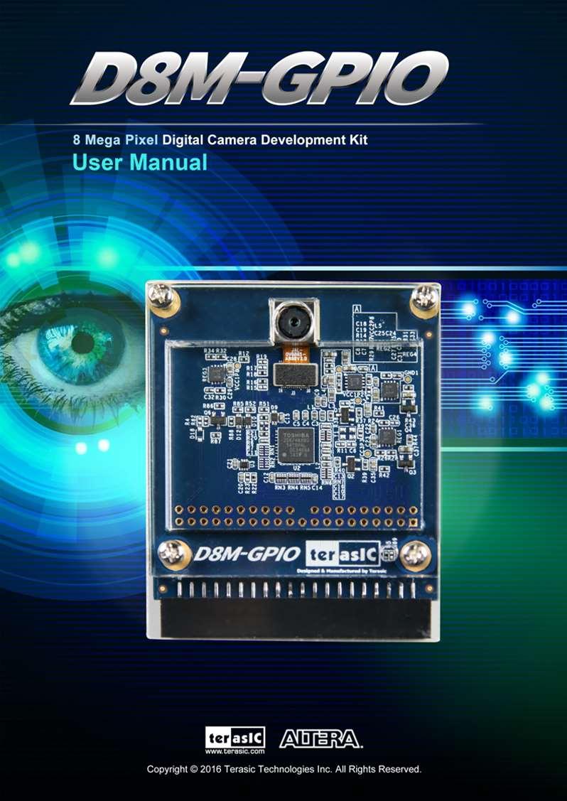
4 Chapter 1 D8M Development Kit Terasic D8M is an 8 Mega Pixel Digital Camera Development Package. The user can connect this camera module onto the FPGA development kit via the 2x20 Pin GPIO connector for image capturing, image processing & image output. The D8M provides the Camera Module with the high speed MIPI interface, which also supports the simple 10Bit Parallel Bayer Pattern Data solution after the MIPI Decoder conversion. It is able to control the D8M module by FPGA via I2C interface for output resolution, ALBC, Frame rate, etc. The D8M also features an Auto-focus function. We do provide demo source codes for the D8M working with different FPGA development kits. These demos are created by using RTL & ALTERA VIP, By referring these demos, the user can quickly learn how to work with this D8M on his/her own application. 1.1 Package Contents Figure 1-1 The D8M package contents The D8M package includes: Product Box 4

5 System CD Download Guide One D8M Module 40-Pin IDC To Box Header Cable 1.2 D8M System CD The D8M System CD contains all the documents and supporting materials associated with D8M, including the user manual, reference designs, and device datasheets. Users can download this system CD from the link: Assemble the Camera Terasic D8M is able to connect on to any FPGA development kit that is equiped with a 2x20 Pin GPIO connector. The pictures below show the connections allowing the D8M to connect to 3 different Terasic FPGA Boards: Figure 1-2 Connect the D8M to DE2-115 board s expansion port 5


6 Figure 1-3 Connect the D8M to DE1-SoC board s expansion port Figure 1-4 Connect the D8M to C5G board s expansion port 1.4 Getting Help Here are the addresses where you can get help if you encounter any problems: Terasic Technologies 9F., No.176, Sec.2, Gongdao 5th Rd, East Dist, Hsinchu City, Taiwan support@terasic.com Tel.: Website: 6

7 Chapter 2 Introduction of the D8M Board 2.1 Features Figure 2 1 shows a photograph of the board. Figure 2-1 shows a photograph of the board. The D8M board has many features that allow users to implement a wide range of designed circuits, from simple circuits to various multimedia projects. The following hardware is provided on the board: Package Interface:2x20 GPIO, 3.3V I/O-standard. MIPI Camera Module: Chip P/N:OV8865 Color Filter Arrangement:Bayer Pattern View Angel:70 Pixels:3268x2448 (8-Mega Pixels) Frame Rate:8-Mega Support Focus Control Programmable controls for frame rate, mirror and flip, cropping, and windowing MIPI Decoder: Chip P/N:TC358748XBG MIPI CSI-2 Compliant 7

8 MIPI to Parallel Port Converter Supports up to 4 data lanes Package Size:73.4x60.0 mm Package Size:73.4x60.0 mm 2.2 Block Diagram of the D8M Board Below Figure 2-2 shows the D8M Block Diagram. MIPI Camera Module outputs 4 Lanes MIPI interface image data, which can be converted to Parallel data by passing through the MIPI Decoder IC to the GPIO interface. Both MIPI Camera Module and MIPI Decoder can be controlled by FPGA I2C interface. Figure 2-2 Block diagram of D8M Board 8

9 Chapter 3 Using the D8M Board This chapter provides instructions on how to use the MIPI camera module, MIPI Decoder and GPIO connector on the D8M board. 3.1 MIPI Camera Module Terasic D8M board equips with an 8M pixel MIPI camera module named OV8865 (See Figure 3-1). The OV8865 color image sensor is a high performance, 8 megapixel RAW image sensor that delivers 3264x2448. It provides options for multiple resolutions while maintaining full field of view. Users can program image resolution, frame rate, and image quality parameters. Camera functions are controlled via I2C bus (CAMERA_I2C_SDA and CAMERA_I2C_SCL). The I2C device address is 0x6C. Figure 3-1 MIPI Camera Module Figure 3-2 shows a cross-section of the image sensor array. The color filter is arranged in a Bayer pattern. Of the 8,332,288 pixels, 7990,272 (3264x2448) are active pixels and can be output. The other pixels are used for black level calibration and interpolation. 9
 driver chip named VCM149C on the MIPI camera module.")
10 Figure 3-2 Sensor Array Region color filter Layout (From Camera Datasheet) For more hardware description and register information about this camera module, please refer to the datasheet named OV8865 Data Sheet.pdf in the D8M System CD. In addition, there is a Voice Coil Motor (VCM) driver chip named VCM149C on the MIPI camera module. Users can use the same I2C bus (I2C device address is 0x18) to modify the DAC value in the VCM driver chip that can allow the VCM to move its lens to the desired position for getting a sharp image and realizing the Auto Focus (AF) feature. Terasic also provides an AF demonstration and IP in the System CD. See section 4.x for details. The datasheet of this VMC driver IC named VM149C VCM Driver IC.pdf also can be found in the System CD. 10
. Decoder users can quickly obtain the image data and process it. MIPI Decoder can convert MIPI Interface up to 24-bit data.")
11 3.2 MIPI Decoder The MIPI camera module output interface is MIPI interface, which cannot directly connect to the Terasic FPGA board; therefore, a MIPI Decoder (TC358748XBG) is added to convert MIPI interface to a parallel port interface (See Figure 3-3). Decoder users can quickly obtain the image data and process it. MIPI Decoder can convert MIPI Interface up to 24-bit data. The Camera module used on the D8M can only output 10 bit data, MIPI_PIXEL_D[9:0] the GPIO connector is the camera image output data bus, and MIPI_PIXEL_D[13:10] is reserved for an alternative camera module with more output bits. Figure 3-3 System Overview with MIPI Decoder in CSI-2 RX to Parallel Port Configuration FPGA also can read/write MIPI Decoder through a I2C bus (MIPI_I2C_SDA / MIPI_I2C_SCL ; I2C device address is 0x1C), which is different from the camera module I2C bus. On the D8M board, MIPI Decoder can output clocks to the MIPI camera and FPGA board. So in the demonstrations, most of them show how to control IC PLL parameters as well as others. You can refer to section 3-4 clock tree for details. 11

12 3.3 GPIO Connector Figure 3-4 and Table 3-1 shows the pin out and pin definitions of the GPIO connector. Figure 3-4 Pin-out of the 40-pin connector on D8M Table 3-1 Pin Assignment of D8M GPIO Interface Signal Name Connector Pin No. Description Pin Direction I/O Standard MIPI_PIXEL_D[0] 4 Parallel Port Data Output 3.3V MIPI_PIXEL_D[1] 5 Parallel Port Data Output 3.3V MIPI_PIXEL_D[2] 6 Parallel Port Data Output 3.3V MIPI_PIXEL_D[3] 7 Parallel Port Data Output 3.3V MIPI_PIXEL_D[4] 8 Parallel Port Data Output 3.3V MIPI_PIXEL_D[5] 9 Parallel Port Data Output 3.3V MIPI_PIXEL_D[6] 10 Parallel Port Data Output 3.3V MIPI_PIXEL_D[7] 13 Parallel Port Data Output 3.3V MIPI_PIXEL_D[8] 14 Parallel Port Data Output 3.3V MIPI_PIXEL_D[9] 15 Parallel Port Data Output 3.3V MIPI_PIXEL_D[10] 16 Reserve Output 3.3V MIPI_PIXEL_D[11] 17 Reserve Output 3.3V MIPI_PIXEL_D[12] 18 Reserve Output 3.3V MIPI_PIXEL_D[13] 22 Reserve Output 3.3V MIPI_RESET_n 27 Master Reset signal for MIPI Input 3.3V 12
13 camera and bridge device MIPI_PIXEL_CLK 2 Parallel Port Clock signal Output 3.3V MIPI_PIXEL_HS 25 Parallel Port Horizontal Synchronization signal Output 3.3V MIPI_PIXEL_VS 23 Parallel Port Vertical Synchronization signal Output 3.3V MIPI_CS_n 26 Chip Select Input 3.3V MIPI_REFCLK 21 Reference Clock Input of bridge device Input 3.3V MIPI_I2C_SCL 35 I2C Clock for bridge device Input 3.3V MIPI_I2C_SDA 36 I2C Data for bridge device Inout 3.3V CAMERA_PWDN_ Power Down signal of MIPI 28 n camera Input 3.3V CAMERA_I2C_SCL 31 I2C Clock for MIPI camera Input 3.3V CAMERA_I2C_SD A 32 I2C Data for MIPI camera Inout 3.3V VCC5 11 5V Power Input N/A N/A GND 12, 30 Ground N/A N/A MIPI_PIXEL_CLK_ RESEVERD 1 Reserve N/A N/A MIPI_MCLK 33 Reserve N/A N/A CAMERA_RESV_P IN 39 Reserve N/A N/A Table3-2 shows the High/Low value of Input/Output Voltage Level on D8M GPIO digital Interface. Table 3-2 DC Electrical Specification Parameter Symbol Min. Max. Unit Input voltage, High level input VIH V Input voltage, Low level input VIL V Output voltage High level VOH V Output voltage Low level VOL V 13
 and outputs Clock to Camera sensor (MCLK), at the same time, MIPI Decoder PLL will also output a parallel port clock (MIPI_PIXEL_CLK) and")
14 3.4 Clock Tree Figure 3-5 is the D8M board clock tree block diagram. MIPI Decoder PLL receives FPGA Reference Clock (MIPI_REFCLK) and outputs Clock to Camera sensor (MCLK), at the same time, MIPI Decoder PLL will also output a parallel port clock (MIPI_PIXEL_CLK) and feedback to the FPGA to deal with parallel data. Figure 3-5 Simple Clock Tree of the D8M Board In the provided demonstrations, MIPI_REFCLK is set to 20MHz, FPGA transmits this clock to the D8M MIPI Decoder PLL through the GPIO connector. No matter how much the camera resolution is, the MCLK fixed output is 25MHz. According to the output resolution, MIPI_PIXEL_CLK can be set as 25MHz for 640x480@60fps and 50MHz for 1920x1080@15fps. For more MIPI Decoder PLL setting details, please refer to TC358746AXBG_748XBG_rev09.pdf "Chapter 5: Clock and System" or refer to Terasic demonstrations. 3.5 Camera Configuration The developers should configure the camera OV8865 via I2C so the camera can output desired image format. To get a better image quality, the following register settings are strongly recommended. These settings are all applied in the CD demo code. For detail information about the registers, please refer the OV8865 datasheet included in the System CD. 14
15 Register Register Description Address Value 0x4011 0x30 Enable the entering of a BLC (black level calibration) offset. 0x4013 0xCF BLC offset value. 0x3508 0x03 Increase the analog gain a bit to compensate for the BLC offset. 0x5000 0x16 Turn off the LENC (lens correction) compensation. This setting creates a very even light distribution across the screen. 15
16 Chapter 4 RTL Example Codes This chapter provides instructions on how to capture a D8M image (resolution is 640X480@60 Hz) and use two storage methods (Line-Buffer and Frame-Buffer) to display the image on a VGA Monitor. These storage methods realized by pure Verilog HDL language have been validated on both DE1-SoC and DE2-115 board. 4.1 Using LINE- BUFFER If the D8M resolution is set to 640x480@60Hz to output to VGA, as both image capturing frequency and VGA output frequency are 60Hz, there is no need to use Frame-Buffer to convert the frame rate, just adjust the frequency difference of the Line-Buffer D8M pixel clock and VGA pixel clock. This demo mainly uses three separate Line Buffers to do the frequency difference adjustment, at the same time, Line Buffer are also used to store the data of converting image from RAW data to RGB data. Function Block Diagram Figure 4-1 is the function block diagram of this demonstration. This demo uses three Line-Buffers to store D8M 640x480@60 Hz raw data, and then extract two of the Line-Buffers raw data to convert it to RGB data and output it to VGA with 640x480@60 Hz timing. This is how VGA Monitor can display the D8M capturing image. In this block, it also provides an auto-focusing module, monitor D8M frame rate module, as well as a pixel clock module. All module functions are described below: MIPI_BRIDGE_CAMERA_Config: the D8M I2C setting controller, such as set D8M to output 640X480@60Hz timing. It mainly writes I2C corresponding parameters to D8M MIPI decoder IC register and Camera Sensor IC register respectively through their own I2C buses. MIPI_I2C bus is used to write MIPI decoder IC (I2C Slave Address = 0x1c.), CAMERA_I2C bus is used to write Camera Sensor (IC Slave Address = 0x6c). 16

17 Figure 4-1 Block diagram of the digital camera D8M design with Line -Buffer D8M_SET: This module is used to process D8M raw data. It includes three Line-Buffers that are used to store raw data, and two of the Line-Buffers raw data will be extracted and converted to RGB data, the Line-Buffer is also used to adjust the frequency difference between D8M and VGA. VGA_Controller_trig: the VGA signal timing generator, can generate Hz signal timing. FOCUS_ADJ: This module provides two main functions. The first function is using I2C bus to write D8M Voice Coil Motor (VCM) driver IC register, and control the camera lens movements to perform image focusing. VCM driver IC register (I2C Slave Address =0x18) shares I2C bus with camera module. The other function is doing the current image high frequency component statistic. When the VCM drives the camera lens movement, a real-time statistics of image high-frequency sum will be done in every step of the moving. Finally, the lens will move to a position which has the largest number of high frequency to complete the automatic focus operation. Focus area can be selected by SW3. There are two options: o Select focusing the whole screen area (set SW3 to 0) o Select focusing the middle area (set SW3 to 1). Once you set SW3 to a value (0 or 1) and press KEY3 one time, the automatic focus operation will be performed in the selected area. FpsMonitor: This module will count D8M MIPI_PIXEL_VS signal pulses in 1 17
 to 1Hz to display on LEDs. Users can observe the LEDs to see if the clocks work or not.")
18 second (it stands fps number) and convert the number to a decimal number to display on two seven-section LEDs. CLOCKMEM: This module will divide the three clocks (VGA_CLK, MIPI_REFCLK and MIPI_PIXEL_CLK) to 1Hz to display on LEDs. Users can observe the LEDs to see if the clocks work or not. We provide the Line-Buffer demonstrations on both DE1-SoC and DE The switch setting and Key operation are the same on both DE1-SoC and DE The following are the descriptions of the two platforms set up, as well as the test steps. DE1-SoC Demonstration: Hardware Setting Up As shown in Figure 4-2 Figure 4-2 DE1-SoC demo hardware setting up Design Tools Quartus II v15.0 Demonstration Source Code Quartus project directory: DE1_SOC_D8M_LB_RTL Nios II Eclipse project workspace: DE1_SOC_D8M_LB_RTL.sof 18
19 Demonstration Batch File Demo batch file folder: demonstrations\ DE1_SOC_D8M_LB_RTL\demo_batch Demonstration Setup Connect the DE1-SoC board (J13) to the host PC with a USB cable and install the USB-Blaster II driver if necessary. Plug D8M onto DE1-SoC JP2(GPIO 1), connect VGA monitor to J9 see Figure 4-2. Plug the 12V adapter to DE1-SoC Board. Power on the DE1-SOC board. Execute the demo batch file test.bat from the directory\ DE1_SOC_D8M_LB_RTL\demo_batch. LED0~1 light up, stand the settings of D8M MIPI decoder IC and Camera Sensor I2C are completed. LED7~9 blink in 1Hz, stand VGA_CLK, MIPI_REFCLK and MIPI_PIXEL_CLK are generated correctly. HEX1~0 decimal number 60 stands D8M camera sensor capturing frame rate is 60Hz. D8M capturing image displays on VGA monitor, if the VGA monitor image is fuzzy, please press Key3 one time again (will perform the focus operation again). Users can switch SW3 to 1 (there will be a yellow box on image), then, press KEY3 one time again, the middle area focus operation will be performed. Table 4-1 summarizes the functional keys and details of each LED status. Table 4-1 The functional keys of the digital camera demonstration Name Description LED0 Lights up when MIPI DECODER I2C setting is successful LED1 Lights up when CAMERA I2C setting is successful LED7 Blink in 1HZ ( VGA CLOCK/25M ) LED8 Blink in 1HZ (D8M REF CLOCK / 20M) LED9 Blink in 1HZ (D8M PIXE CLOCK /50M) HEX1-0 Display FRAME RATE in two decimal number KEY0 SYSTEM RESET KEY3 Image auto focus(area based on SW3 selection) SW3 0: No yellow box (focus on whole screen area) 1: There is a yellow box(focus on yellow box) 19

20 DE2-115 Demonstration: Hardware Setting Up As shown in Figure 4-3 Figure 4-3 DE2-115 demo hardware setting up Design Tools Quartus II v15.0 Demonstration Source Code Quartus project directory: DE2_115_D8M_LB_RTL Nios II Eclipse project workspace: DE2_115_D8M_LB_RTL.sof Demonstration Batch File Demo batch file folder: Demonstrations\ DE2_115_D8M_LB_RTL \demo_batch Demonstration Setup Connect the DE2-115 board (J9) to the host PC with a USB cable and install the USB-Blaster II driver if necessary. Plug D8M onto DE2-115 JP5 (GPIO), connect VGA monitor to J13 (VGA) see Figure 4-3. Plug the 12V adapter to DE2-115 Board. 20
21 Power on the DE2-115 board. Execute the demo batch file test.bat from the directory\ DE2_115_D8M_LB_RTL\demo_batch. LED0~1 light up, stand the settings of D8M MIPI decoder IC and Camera Sensor I2C are completed. LED7~9 blink in 1Hz, stand VGA_CLK, MIPI_REFCLK and MIPI_PIXEL_CLK are generated correctly. HEX1~0 decimal number 60 stands D8M camera sensor capturing frame rate is 60Hz. D8M capturing image displays on VGA monitor, if the VGA monitor image is fuzzy, please press Key3 one time again (will perform the focus operation again). Users can switch SW3 to 1 (there will be a yellow box on image), then, press SW3 one time again, the middle area focus operation will be performed. Table 4-2 summarizes the functional keys and details of each LED status Table 4-2 The functional keys of the digital camera demonstration Name Description LED0 Lights up when MIPI DECODER I2C setting is successful LED1 Lights up when CAMERA I2C setting is successful LED7 Blink in 1HZ ( VGA CLOCK/25M ) LED8 Blink in 1HZ (D8M REF CLOCK / 20M) LED9 Blink in 1HZ (D8M PIXE CLOCK /50M) HEX1-0 Display FRAME RATE in two decimal number KEY0 SYSTEM RESET KEY3 Image auto focus(area based on SW3 selection) SW3 0: No yellow box (focus on whole screen area) 1: There is a yellow box(focus on yellow box) 4.2 Using FRAME - BUFFER This section provides instructions on how to store D8M capturing image(640x480@60 Hz)in a larger memory(frame-buffer, this Memory is expected to store up to one Frame image), and how to extract Frame-Buffer address data to convert RAW data to VGA data, and output the VGA data to VGA monitor with 640x480@60 Hz VGA timing. Function Block Diagram 21

22 Figure 4-4 is the function block diagram of this demonstration. This design block is similar to Line-Buffer s. The only difference is one more Sdram_Control module is there. This module can control general external SDRAM Memory and read/write image data. As shown in the block diagram, D8M raw data will be written in SDRAM first. After finishing writing a Frame, Sdram_Control module will read out the data from SDRAM to RAW2RGB_J module to convert RAW data to RGB data. The RGB data will output along with the signal timing generated by VGA_Controller to VGA monitor. In the block, other module (for example, FOCUS_ADJ, MIPI_BRIDGE_CAMERA_Config, FpsMonitor, CLOCKMEM) function instructions and KEY/SW operations are the same with Line-Buffer s: Figure 4-4 Block diagram of the digital camera D8M design with Frame -Buffer We provide the Frame-Buffer demonstrations on both DE1-SoC and DE And the display resolution is 640x480@60Hz too. The demonstration setting up methods are the same with section 4.1.Please see following instructions for details. DE1-SoC Demonstration: Design Tools Quartus II v15.0 Demonstration Source Code 22
23 Quartus project directory: Project directory: DE1_SOC_D8M_RTL Nios II Eclipse project workspace: Bitstream used: DE1_SOC_D8M_RTL.sof Demonstration Batch File Demo batch file folder: demonstrations\ DE1_SOC_D8M_RTL \demo_batch Demonstration Setup Connect the DE1-SoC board (J13) to the host PC with a USB cable and install the USB-Blaster II driver if necessary. Plug D8M onto DE1-SoC JP2 (GPIO 1), connect VGA monitor to J9 see Figure 4-2. Plug the 12V adapter to DE1-SoC Board. Power on the DE1-SOC board. Execute the demo batch file test.bat from the directory\ DE1_SOC_D8M_RTL\demo_batch. Below operations are the same with section 4.1 DE1_SoC Line-Buffer Demo. DE2-115 Demonstration: Design Tools Quartus II v15.0 Demonstration Source Code Quartus project directory: DE2_115_D8M_RTL Nios II Eclipse project workspace: DE2_115_D8M_RTL.sof Demonstration Batch File Demo batch file folder: Demonstrations\ DE2_115_D8M_RTL \demo_batch Demonstration Setup Connect the DE2-115 board (J9) to the host PC with a USB cable and install the USB-Blaster II driver if necessary. Plug D8M onto DE2-115 JP5 (GPIO), connect VGA monitor to J13 (VGA) see Figure 4 3. Plug the 12V adapter to DE2-115 Board. Power on the DE2-115 board. Execute the demo batch file test.bat from the directory\ DE2_115_D8M_RTL\demo_batch. Below operations are the same with section 4.1 DE2_115 Line-Buffer Dem 23
24 Chapter 5 NIOS Based Example Codes This chapter provides several NIOS based examples for users to get started using the D8M board. 5.1 DE1_SOC and DE2-115 D8M_VIP Demonstration This demonstration shows how to implement a D8M on DE1-SoC and DE2-115 Boards. The Altera VIP (Video Image Processing) suite is used to display image/s on the VGA monitor. The Nios II processor is used to configure the I2C devices. There is a Camera IP from Terasic in Qsys, which translates the Bayer pattern from the camera to the RGB video steam format and feeds it to the Altera VIP. The other IP developed by Terasic for auto-focus is used to find the optimized focus settings of the user-defined image area. Function Block Diagram DE1_SOC_D8M_VIP reference design is developed based on Altera s Video and Image Processing (VIP) suite. The Terasic Camera IP translates the parallel Bayer pattern data into RGB data to meet the specification of the Altera VIP video streaming. The Frame Buffer from VIP is used for buffering image data in DDR3 and matching the frame rate from the Terasic camera IP to the Clock Video Output of VIP. It displays the final 640x480 RGB frame image on the VGA Monitor. The auto-focus IP by Terasic can be used to get a better image quality by finding the optimized focus setting. Figure 5-1 shows the Function block diagram of DE1_SOC_D8M_VIP demonstration. 24
25 Figure 5-1 Function block diagram of DE1_SOC_D8M_VIP demonstration The Nios II program running the on-chip memory controls the I2C controllers to configure the image sensor, motor driver, and the MIPI Decoder IC. The first I2C controller is used to configure the camera module, including the OV8865 image sensor and the VCM149C. The second I2C controller is used to configure the MIPI Decoder TC358748XBG. Note: The focus driver IC (VCM149C) in the camera module is also configured by the Terasic auto-focus IP through its own I2C master controller. Users must make sure there is only one I2C master used one at a time. The default camera settings In this demonstration, the default camera settings are: Resolution: 600x480 Frame Rate: 60 fps Pixel Data: RAW10 Bin Mode: 1, 2, 4 (achieved ZOOM-IN/ ZOOM-OUT function) Users can change the settings base on their requirements. Design Tools 25
26 Quartus II v15.0 Nios II Eclipse 15.0 Demonstration Source Code Quartus project directory: DE1_SOC_D8M_VIP Nios II Eclipse project workspace: DE1_SOC_D8M_VIP\software Demonstration Batch File Demo batch file folder: demonstrations\de1_soc_d8m_vip\demo_batch Demonstration Setup Connect a USB cable between the host PC and the USB connector (J13) on the DE1-SOC board (See Figure 5-2). Connect D8M module to GPIO1 (JP2) on DE1-SOC board. Connect the VGA output of the DE1-SOC board to a VGA monitor. Power on the DE1-SOC board. Execute the demo batch file test.bat under the batch file folder DE1_SOC_D8M_VIP\demo_batch. The VGA Monitor will start showing the video captured from the camera. Press KEY0 to trigger the auto-focus function. Press KEY1/2 to trigger the manual focus adjustment. Press KEY3 to trigger the ZOOM function. Table 5-1 summarizes the functional keys. Figure 5-2 Setup Connection of DE1_SOC_D8M_VIP demonstration 26
![Table 5-1 The functional keys of the digital camera demonstration Component KEY0 Function Description Trigger AutoFocus KEY1 Trigger Manual focus - KEY2 Trigger Manual focus + KEY3 HEX[1:0] Trigger](/docs-images/81/84263365/images/27-0.jpg "ZOOM function fps (frames per sencond) Demonstration Setup for DE2-115 board Users can also use the same Qsys and Altera VIP framework on the D8M and the DE2-115 boards.")
27 Table 5-1 The functional keys of the digital camera demonstration Component KEY0 Function Description Trigger AutoFocus KEY1 Trigger Manual focus - KEY2 Trigger Manual focus + KEY3 HEX[1:0] Trigger ZOOM function fps (frames per sencond) Demonstration Setup for DE2-115 board Users can also use the same Qsys and Altera VIP framework on the D8M and the DE2-115 boards. Please refer to Figure 5-3 for hardware setup. The set up steps are described below: Figure 5-3 DE2-115 demo hardware setting up Connect the DE2-115 board (J9) to the host PC with a USB cable and install the USB-Blaster II driver if necessary. Plug the D8M onto the DE2-115 JP5 (GPIO), and connect the VGA monitor to J13 (VGA). 27
28 Plug the 12V adapter to the DE2-115 Board. Power on the DE2-115 board. Execute the demo batch file DE2_115_D8M.bat under the batch file folder DE2_115_D8M_VIP\demo_batch. Press KEY0 to trigger autofocus function. Press KEY1/2 to trigger manual focus adjustment. Press KEY3 to trigger ZOOM function. Table 5-1 summarizes the functional keys. 5.2 DE1_SOC_D8Mx2_VIP Demonstration This demonstration shows how to implement two D8M boards in DE1-SoC. Two D8M streaming processed and mixed by the Altera VIP (Video Image Processing) suite and finally displays images on the VGA monitor. Function Block Diagram Figure 5-4 shows the Function block diagram of DE1_SOC_D8MX2_VIP demonstration. 28

29 Figure 5-4 Function block diagram of DE1_SOC_D8MX2_VIP demonstration DE1_SOC_D8MX2_VIP reference design is developed based on Altera s Video and Image Processing (VIP) suite. This demo implements two D8M boards and outputs their parallel images data into the FPGA. Insside the FPGA, image data will enter the Terasic Camera IP, Cliper, Terasic AutoFocus and Scaller blocks sequentially. After that, 10bit RAW data will be converted to 24-bit RGB data (in 640x480 resolution) and stored into the SDRAM as a cache via the Frame Buffer block. Then, these two image streams will be read and blended together (in 800x600 resolution) by Mixer IP. Finally it displays on the VGA monitor via Clock Video Output block. The Nios II program running the on-chip memory controls on the two I2C controllers to configure the image sensor, motor driver, and the MIPI CSI-2 Decoder IC. Note: The focus driver IC (VCM149C) in the camera module is also configured by the 29
30 Terasic auto-focus IP through its own I2C master controller. Users must make sure there is only one I2C master used a time. KEY IP Descriptions In this demonstration, the default camera settings are: Terasic Camera IP implements RAW to RGB and avalon-st streaming package conversion. Terasic AutoFocus IP implements Simplified AutoFocus function. Scaler IP implements Scaling function. Combining with software configuration, it can scale two 640x480 images to proper size to fit the bandwidth limitations (100MHz x 16bit) of the SDRAM. Frame Buffer IP can read and write image stream into the SDRAM Mixer IP Camera will blend two image data into one picture (resolution is 800x600). Clock Video Output block will output the image data (resolution is 800x600) from the Mixer IP to the VGA monitor. The default camera settings In this demonstration, the default camera settings are: Resolution: 600x480 Frame Rate: 50 fps Pixel Data: RAW10 Bin Mode: 1, 2, 4 (achieved ZOOM-IN/ ZOOM-OUT function) Camera1 default settings: Resolution: 600x480 Frame Rate: 50 fps Pixel Data: RAW10 Bin Mode: 1, 2, 4 (achieved ZOOM-IN/ ZOOM-OUT function) Users can change the settings base on their requirements. Synchronize Two D8M Data Streaming There is a simple way to synchronize multiple D8M s Frame Start signals. See Table 5-2 follow the Hardware standby with PWDNB mode. After configuring all of the D8M s registers, just pulling all of the D8M s PWDNB signal low for a while at the same time. In this way, the register setting will not be clear and it will synchronize all 30
31 the D8M s Frame Star. Table 5-2 Hardware and Standby Description Mode Description Enable by pulling PWDNB low Input clock is gated by PWDNB, no SCCB communication Hardware standby with PWDNB Register value are maintained Power down all blocks and regulator Low power consumption GPIO can be configured as high/low/tri-state Design Tools Quartus II v15.0 Nios II Eclipse 15.0 Demonstration Source Code Quartus project directory: DE1_SOC_D8MX2_VIP Nios II Eclipse project workspace: DE1_SOC_D8M_VIP\software Demonstration Batch File Demo batch file folder: demonstrations\de1_soc_d8mx2_vip\demo_batch Demonstration Setup Connect a USB cable between the host PC and the USB connector (J13) on the DE1-SOC board. Connect the two D8M modules to GPIO0 (JP1) and GPIO1 (JP2) on DE1-SOC board (See Figure 5-5). Connect the VGA output of the DE1-SOC board to a VGA monitor. 31
 Press KEY0 to trigger autofocus function.")

32 Figure 5-5 Function block diagram of DE1_SOC_D8MX2_VIP demonstration Power on the DE1-SOC board. Execute the demo batch file test.bat under the batch file folder DE1_SOC_D8M_VIP\demo_batch. The VGA Monitor will start showing the video captured from the camera. Put SW1 to low position(camera Function) Press KEY0 to trigger autofocus function. Press KEY1/2 to trigger manual focus adjustment. Press KEY3 to trigger ZOOM function. Note SW0 high to configure camera 1,SW0 low to configure camera 0 Put SW1 to high position (Mixer Function). Press KEY0 to trigger display mode change as shown in Figure 5-6. Figure 5-6 Four display modes in Mixer function. Press KEY1/2 to scale camera video to left/right position (See Figure 5-7) or upper left / lower right position (See Figure 5-8). 32
 or camera1 (SW0 in high position) function. Note : Put SW0 to high position to configure camera1, put SW0 to low position to configure camera0.")
33 Figure 5-7 Scale video size of camera0 or camera1 on left/right position Figure 5-8 Scale video size of camera0 or camera1 in the upper left or lower right position Press KEY3 to trigger Stop/Run camera0 (SW0 in low position) or camera1 (SW0 in high position) function. Note : Put SW0 to high position to configure camera1, put SW0 to low position to configure camera0. Table 5-3 summarizes the functional keys. 33
34 Table 5-3 The functional keys of the digital camera demonstration Function Description Component SW1 low: Camera Function SW1 high: Mixer Function KEY0 Trigger AutoFocus display mode change KEY1 Trigger Manual focus - Scale camera video to right/bottom KEY2 Trigger Manual focus + Scale camera video to left/top KEY3 Trigger ZOOM function Stop/Run camera0/1 SW0 SW1 HEX[1:0] Camera configure select: high: configure Camera 1 low : configure Camera 0 KEY0-3 function switch fps (frames per sencond) 5.3 C5G_D8M_VIP Demonstration This demonstration shows how to implement a camera demo in Altera Qsys tool. Altera VIP (Video Image Processing) suite is used to display the image on the HDMI monitor and the Nios II processor is used to configure the I2C devices. There is a Camera IP from Terasic in Qsys, which translates the Bayer pattern from camera to the RGB video steam format, and feeds it to Altera VIP. The other IP developed by Terasic for auto-focus is used to find the optimized focus settings of user-defined image area. Function Block Diagram Figure 5-9 shows the Function block diagram of C5G_D8M_VIP demonstration. 34

35 Figure 5-9 Function block diagram of C5G_D8M_VIP demonstration C5G_D8M_VIP reference design is developed based on Altera s Video and Image Processing (VIP) suite. The Terasic Camera IP translates the parallel Bayer pattern data into RGB data to meet the specification of the Altera VIP video streaming. The Frame Buffer from the VIP is used for buffering image data in DDR3 and matching the frame rate from the Terasic camera IP to the Clock Video Output of the VIP. It displays the final 640x480 RGB frame image on the HDMI monitor. The auto-focus IP by Terasic can be used to get a better image quality by finding the optimized focus setting. The Nios II program running the on-chip memory controls the two I2C controllers to configure the image sensor, motor driver, and the MIPI Decoder IC. The first I2C controller is used to configure the camera module, including the OV8865 image sensor and the VCM149C. The second I2C controller is used to configure the MIPI Decoder TC358748XBG. Note: The focus driver IC (VCM149C) in the camera module is also configured by the 35
36 Terasic auto-focus IP through its own I2C master controller. Users must make sure there is only one I2C master used at a time. The default camera settings In this demonstration, the default camera settings are: Resolution: 1920x1080 Frame Rate: 15 fps Pixel Data: RAW10 Bin Mode: 1, 2, 4 (achieved ZOOM-IN/ ZOOM-OUT function) Users can change the settings base on their requirements. Design Tools Quartus II v15.0 Nios II Eclipse 15.0 Demonstration Source Code Quartus project directory: C5G_D8M_VIP Nios II Eclipse project workspace: C5G_D8M_VIP\software Demonstration Batch File Demo batch file folder: demonstrations\de1_soc_d8m_vip\demo_batch Demonstration Setup Switch the Dip Switch S1/S2 which is located on the back of the board to the "OFF" position. Connect a USB cable between the host PC and the USB connector (J10) on the C5G board (See Figure 5-10). Connect D8M module in GPIO0(JP9) on C5G board. Connect the VGA output of the C5G board to a HDMI monitor. Power on the C5G board. Execute the demo batch file test.bat under the batch file folder C5G_D8M_VIP\demo_batch. The HDMI monitor will start showing the video captured from the camera. Press KEY0 to trigger autofocus function. Press KEY1/2 to trigger manual focus adjustment. Table 5-4 summarizes the functional keys. 36

37 Figure 5-10 Setup Connection of DE1_SOC_D8M_VIP demonstration Table 5-4 The functional keys of the digital camera demonstration Component KEY0 Function Description Trigger AutoFocus KEY1 Trigger Manual focus - KEY2 Trigger Manual focus + KEY3 HEX[1:0] Trigger ZOOM function fps (frames per sencond) 37
38 Chapter 6 Appendix 6.1 Revision History Version Change Log V1.0 Initial Version V1.0.1 Modify Figure 3-1 V1.0.2 Modify Support information and page21 V1.1.0 Add recommend register setting for camera V1.1.1 Modify Figure Copyright Statement Copyright 2018 All rights reserved. 38
Chapter 1 HDMI-FMC Development Kit Chapter 2 Introduction of the HDMI-FMC Card Chapter 3 Using the HDMI-FMC Board...
 Chapter 1 HDMI-FMC Development Kit... 2 1-1 Package Contents... 3 1-2 HDMI-FMC System CD... 3 1-3 Getting Help... 3 Chapter 2 Introduction of the HDMI-FMC Card... 4 2-1 Features... 5 2-2 Block Diagram
Lattice Embedded Vision Development Kit User Guide
 FPGA-UG-02015 Version 1.1 January 2018 Contents Acronyms in This Document... 3 1. Introduction... 4 2. Functional Description... 5 CrossLink... 5 ECP5... 6 SiI1136... 6 3. Demo Requirements... 7 CrossLink
SingMai Electronics SM06. Advanced Composite Video Interface: HD-SDI to acvi converter module. User Manual. Revision 0.
 SM06 Advanced Composite Video Interface: HD-SDI to acvi converter module User Manual Revision 0.4 1 st May 2017 Page 1 of 26 Revision History Date Revisions Version 17-07-2016 First Draft. 0.1 28-08-2016
SingMai Electronics SM06. Advanced Composite Video Interface: DVI/HD-SDI to acvi converter module. User Manual. Revision th December 2016
 SM06 Advanced Composite Video Interface: DVI/HD-SDI to acvi converter module User Manual Revision 0.3 30 th December 2016 Page 1 of 23 Revision History Date Revisions Version 17-07-2016 First Draft. 0.1
AN 776: Intel Arria 10 UHD Video Reference Design
 AN 776: Intel Arria 10 UHD Video Reference Design Subscribe Send Feedback Latest document on the web: PDF HTML Contents Contents 1 Intel Arria 10 UHD Video Reference Design... 3 1.1 Intel Arria 10 UHD
Display Interfaces. Display solutions from Inforce. MIPI-DSI to Parallel RGB format
 Display Interfaces Snapdragon processors natively support a few popular graphical displays like MIPI-DSI/LVDS and HDMI or a combination of these. HDMI displays that output any of the standard resolutions
AD9884A Evaluation Kit Documentation
 a (centimeters) AD9884A Evaluation Kit Documentation Includes Documentation for: - AD9884A Evaluation Board - SXGA Panel Driver Board Rev 0 1/4/2000 Evaluation Board Documentation For the AD9884A Purpose
Design and Implementation of an AHB VGA Peripheral
 Design and Implementation of an AHB VGA Peripheral 1 Module Overview Learn about VGA interface; Design and implement an AHB VGA peripheral; Program the peripheral using assembly; Lab Demonstration. System
Sundance Multiprocessor Technology Limited. Capture Demo For Intech Unit / Module Number: C Hong. EVP6472 Intech Demo. Abstract
 Sundance Multiprocessor Technology Limited EVP6472 Intech Demo Unit / Module Description: Capture Demo For Intech Unit / Module Number: EVP6472-SMT949 Document Issue Number 1.1 Issue Data: 27th April 2012
Bitec. HSMC Quad Video Mosaic Reference Design. DSP Solutions for Industry & Research. Version 0.1
 Bitec DSP Solutions for Industry & Research HSMC Quad Video Mosaic Reference Design Version 0.1 Page 2 Revision history... 3 Introduction... 4 Installation... 5 Building the demo software... 6 Page 3 Revision
Group 1. C.J. Silver Geoff Jean Will Petty Cody Baxley
 Group 1 C.J. Silver Geoff Jean Will Petty Cody Baxley Vision Enhancement System 3 cameras Visible, IR, UV Image change functions Shift, Drunken Vision, Photo-negative, Spectrum Shift Function control via
Design and implementation (in VHDL) of a VGA Display and Light Sensor to run on the Nexys4DDR board Report and Signoff due Week 6 (October 4)
 of a VGA Display and Light Sensor to run on the Nexys4DDR board Report and Signoff due Week 6 (October 4)") ECE 574: Modeling and synthesis of digital systems using Verilog and VHDL Fall Semester 2017 Design and implementation (in VHDL) of a VGA Display and Light Sensor to run on the Nexys4DDR board Report and
ECE 574: Modeling and synthesis of digital systems using Verilog and VHDL Fall Semester 2017 Design and implementation (in VHDL) of a VGA Display and Light Sensor to run on the Nexys4DDR board Report and
THDB_ADA. High-Speed A/D and D/A Development Kit
 THDB_ADA High-Speed A/D and D/A Development Kit With complete reference design and source code for Fast-Fourier Transform analysis and arbitrary waveform generator. 1 CONTENTS Chapter 1 About the Kit...2
Alain Legault Hardent. Create Higher Resolution Displays With VESA Display Stream Compression
 Alain Legault Hardent Create Higher Resolution Displays With VESA Display Stream Compression What Is VESA? 2 Why Is VESA Needed? Video In Processor TX Port RX Port Display Module To Display Mobile application
SignalTap Plus System Analyzer
 SignalTap Plus System Analyzer June 2000, ver. 1 Data Sheet Features Simultaneous internal programmable logic device (PLD) and external (board-level) logic analysis 32-channel external logic analyzer 166
Implementing Audio IP in SDI II on Arria V Development Board
 Implementing Audio IP in SDI II on Arria V Development Board AN-697 Subscribe This document describes a reference design that uses the Audio Embed, Audio Extract, Clocked Audio Input and Clocked Audio
FPGA Development for Radar, Radio-Astronomy and Communications
 John-Philip Taylor Room 7.03, Department of Electrical Engineering, Menzies Building, University of Cape Town Cape Town, South Africa 7701 Tel: +27 82 354 6741 email: tyljoh010@myuct.ac.za Internet: http://www.uct.ac.za
JESD204B IP Hardware Checkout Report with AD9250. Revision 0.5
 JESD204B IP Hardware Checkout Report with AD9250 Revision 0.5 November 13, 2013 Table of Contents Revision History... 2 References... 2 1 Introduction... 3 2 Scope... 3 3 Result Key... 3 4 Hardware Setup...
ANALOG TO VGA VIDEO INTERFACE GREGORY M. REDMAN. A technical report submitted to the Graduate School. In partial fulfillment of the requirements
 ANALOG TO VGA VIDEO INTERFACE BY GREGORY M. REDMAN A technical report submitted to the Graduate School In partial fulfillment of the requirements for the degree Master of Sciences, Engineering Specialization
YSC -HD-AK1 HDMI / HD-SDI
 Remote Head Kamera 1/2.7 CMOS 2.14 Megapixel Sensor image memory Video Output 1 HDMI Video Output 2 HD-SDI Video Output 3 HD-SDI signal system 1080p/30fps YSC-HD-AK1 HDMI / HD-SDI POWER HDMI HD-SDI USB
DLP Pico Chipset Interface Manual
 Data Sheet TI DN 2510477 Rev A May 2009 DLP Pico Chipset Interface Manual Data Sheet TI DN 2510477 Rev A May 2009 IMPORTANT NOTICE BEFORE USING TECHNICAL INFORMATION, THE USER SHOULD CAREFULLY READ THE
STAR-07 RGB MULTI-COLOR INDUSTRIAL PATTERN PROJECTION
 STAR-07 RGB MULTI-COLOR INDUSTRIAL PATTERN PROJECTION STAR-07 RGB is a high performance DLP projector based upon the Texas Instruments micromirror technology and designed to serve in demanding industrial
Design and Implementation of SOC VGA Controller Using Spartan-3E FPGA
 Design and Implementation of SOC VGA Controller Using Spartan-3E FPGA 1 ARJUNA RAO UDATHA, 2 B.SUDHAKARA RAO, 3 SUDHAKAR.B. 1 Dept of ECE, PG Scholar, 2 Dept of ECE, Associate Professor, 3 Electronics,
Altera JESD204B IP Core and ADI AD6676 Hardware Checkout Report
 2015.11.02 Altera JESD204B IP Core and ADI AD6676 Hardware Checkout Report AN-753 Subscribe The Altera JESD204B IP Core is a high-speed point-to-point serial interface intellectual property (IP). The JESD204B
microenable IV AS1-PoCL Product Profile of microenable IV AS1-PoCL Datasheet microenable IV AS1-PoCL
 i Product Profile of Scalable, intelligent frame grabber for image acquisition and OEM projects Single channel, Base format frame grabber PoCL SafePower Broad camera support No camera file needed Image
Dual HD-SDI Output (MCX + BNC connector) HD- SDI Cable Driver. HDMI DVI Tx connector. Optical HD- SDI Output LC - connector. 8pin
 HD- SDI Cable Driver. HDMI DVI Tx connector. Optical HD- SDI Output LC - connector. 8pin") Thunder Link is a family of small form factor modules for formatting and converting generic digital video streams to standard compliant formats. Different interface standards are supported from the transmitter
Thunder Link is a family of small form factor modules for formatting and converting generic digital video streams to standard compliant formats. Different interface standards are supported from the transmitter
Aegis Electronic Group
 This is a family of small form factor modules for formatting and converting generic digital video streams to standard compliant formats. Different interface standards are supported from the transmitter
Chapter 1 Introduction of the tpad About the Kit Getting Help Chapter 2 tpad Architecture... 8
 1 CONTENTS Chapter 1 Introduction of the tpad... 2 1.1 About the Kit... 6 1.2 Getting Help... 7 Chapter 2 tpad Architecture... 8 2.1 Layout and Components... 8 2.2 Block Diagram of the tpad... 9 Chapter
Altera JESD204B IP Core and ADI AD9144 Hardware Checkout Report
 2015.12.18 Altera JESD204B IP Core and ADI AD9144 Hardware Checkout Report AN-749 Subscribe The Altera JESD204B IP core is a high-speed point-to-point serial interface intellectual property (IP). The JESD204B
GALILEO Timing Receiver
 GALILEO Timing Receiver The Space Technology GALILEO Timing Receiver is a triple carrier single channel high tracking performances Navigation receiver, specialized for Time and Frequency transfer application.
Sundance Multiprocessor Technology Limited. Capture Demo For Intech Unit / Module Number: C Hong. EVP6472 Intech Demo. Abstract
 Sundance Multiprocessor Technology Limited EVP6472 Intech Demo Unit / Module Description: Capture Demo For Intech Unit / Module Number: EVP6472-SMT909 Document Issue Number 1.1 Issue Data: 25th Augest
CH7053A HDTV/VGA/ DVI Transmitter
 Chrontel Brief Datasheet HDTV/VGA/ DVI Transmitter FEATURES DVI Transmitter support up to 1080p DVI hot plug detection Supports Component YPrPb (HDTV) up to 1080p and analog RGB (VGA) monitor up to 1920x1080
RF4432 wireless transceiver module
 RF4432 wireless transceiver module 1. Description RF4432 adopts Silicon Lab Si4432 RF chip, which is a highly integrated wireless ISM band transceiver. The features of high sensitivity (-121 dbm), +20
Lancelot. VGA video controller for the Altera Nios II processor. V4.0. December 16th, 2005
 Lancelot VGA video controller for the Altera Nios II processor. V4.0 December 16th, 2005 http://www.microtronix.com 1. Description Lancelot is a VGA video controller for the Altera Nios (II) processor.
Modular Video Wall Controller
 Modular Video Wall Controller Feb.12th, 2017 Table of content INTRODUCTION...1 Availability and Reliability... 2 Robustness... 3 Easy Expansion...4 Powerful Video and Image Processing...4 4K Ultra HD Support...4
MIPI D-PHY Bandwidth Matrix Table User Guide. UG110 Version 1.0, June 2015
 UG110 Version 1.0, June 2015 Introduction MIPI D-PHY Bandwidth Matrix Table User Guide As we move from the world of standard-definition to the high-definition and ultra-high-definition, the common parallel
AL37219C-EVB-A2 Evaluation Board
 AL37219C-EVB-A2 Evaluation Board User Manual Version 1.1 INFORMATION FURNISHED BY AVERLOGIC IS BELIEVED TO BE ACCURATE AND RELIABLE. HOWEVER, NO RESPONSIBILITY IS ASSUMED BY AVERLOGIC FOR ITS USE, OR FOR
microenable IV AD1-PoCL Product Profile of microenable IV AD1-PoCL Datasheet microenable IV AD1-PoCL
 i Product Profile of Scalable, intelligent frame grabber for image acquisition and OEM projects Base to Medium incl DualBase format frame grabber PoCL SafePower Broad camera support No camera file needed
microenable 5 marathon ACL Product Profile of microenable 5 marathon ACL Datasheet microenable 5 marathon ACL
 i Product Profile of Scalable, intelligent high performance frame grabber for highest requirements on image acquisition and preprocessing by robust industrial MV standards All formats of Camera Link standard
ECE532 Digital System Design Title: Stereoscopic Depth Detection Using Two Cameras. Final Design Report
 ECE532 Digital System Design Title: Stereoscopic Depth Detection Using Two Cameras Group #4 Prof: Chow, Paul Student 1: Robert An Student 2: Kai Chun Chou Student 3: Mark Sikora April 10 th, 2015 Final
SPI Serial Communication and Nokia 5110 LCD Screen
 8 SPI Serial Communication and Nokia 5110 LCD Screen 8.1 Objectives: Many devices use Serial Communication to communicate with each other. The advantage of serial communication is that it uses relatively
Design and Implementation of Nios II-based LCD Touch Panel Application System
 Design and Implementation of Nios II-based Touch Panel Application System Tong Zhang 1, Wen-Ping Ren 2, Yi-Dian Yin, and Song-Hai Zhang School of Information Science and Technology, Yunnan University No.2,
Quick Guide Book of Sending and receiving card
 Quick Guide Book of Sending and receiving card ----take K10 card for example 1 Hardware connection diagram Here take one module (32x16 pixels), 1 piece of K10 card, HUB75 for example, please refer to the
Design of VGA Controller using VHDL for LCD Display using FPGA
 International OPEN ACCESS Journal Of Modern Engineering Research (IJMER) Design of VGA Controller using VHDL for LCD Display using FPGA Khan Huma Aftab 1, Monauwer Alam 2 1, 2 (Department of ECE, Integral
VGA Pixel Buffer Stephen Just
 VGA Pixel Buffer Stephen Just 2016-02-20 1 Introduction Video output is often a useful addition to interactive projects but typically there have been many performance limitations with respect to video
Sapera LT 8.0 Acquisition Parameters Reference Manual
 Sapera LT 8.0 Acquisition Parameters Reference Manual sensors cameras frame grabbers processors software vision solutions P/N: OC-SAPM-APR00 www.teledynedalsa.com NOTICE 2015 Teledyne DALSA, Inc. All rights
Evaluation Board for CS4954/55
 Evaluation Board for CS4954/55 Features l Demonstrates recommended layout and grounding practices l Supports both parallel and serial digital video input l On-board test pattern generation l Supports NTSC/PAL
HDMI-UVC/HDMI-Parallel converter [SVO-03 U&P]
![HDMI-UVC/HDMI-Parallel converter [SVO-03 U&P]](/thumbs/82/85356025.jpg "HDMI-UVC/HDMI-Parallel converter [SVO-03 U&P]") HDMI-UVC/HDMI-Parallel converter [SVO-03 U&P] Hardware specifications Rev. Net Vision Co., Ltd. SVO-03 U&P hardware specifications Revision history Revision Date Content Charge 1.0 2016/06/08 First edition
HDMI-UVC/HDMI-Parallel converter [SVO-03 U&P] Hardware specifications Rev. Net Vision Co., Ltd. SVO-03 U&P hardware specifications Revision history Revision Date Content Charge 1.0 2016/06/08 First edition
Chrontel CH7015 SDTV / HDTV Encoder
 Chrontel Preliminary Brief Datasheet Chrontel SDTV / HDTV Encoder Features 1.0 GENERAL DESCRIPTION VGA to SDTV conversion supporting graphics resolutions up to 104x768 Analog YPrPb or YCrCb outputs for
CH7520. CH7520 DisplayPort to VGA/HDTV Converter GENERAL DESCRIPTION
 Chrontel Brief Datasheet DisplayPort to VGA/HDTV Converter FEATURES Compliant with DisplayPort (DP) specification version 1.2 Support 2 Main Link Lanes at either 1.62Gb/s or 2.7Gb/s link rate Support multiple
Altera JESD204B IP Core and ADI AD9250 Hardware Checkout Report
 2015.06.25 Altera JESD204B IP Core and ADI AD9250 Hardware Checkout Report AN-JESD204B-AV Subscribe The Altera JESD204B IP core is a high-speed point-to-point serial interface intellectual property (IP).
TL6050 / TL6051 / TL6052 Datasheet - HDMI/HD-SDI Output Video Transceiver. TL605x - Features. Block Diagram TL605x.
 Thunder Link is a family of small form factor modules for formatting and converting generic digital video streams to standard compliant formats. Different interface standards are supported from the transmitter
3G fiber. TL7070 3G/HD-SDI + DVI(HDMI) Fiber plus Coax Output Video Transmitter. TL Features. Block Diagram TL7070
 Fiber plus Coax Output Video Transmitter. TL Features. Block Diagram TL7070") Thunder Link is a family of small form factor modules for formatting and converting generic digital video streams to standard compliant formats. Different interface standards are supported from the transmitter
Thunder Link is a family of small form factor modules for formatting and converting generic digital video streams to standard compliant formats. Different interface standards are supported from the transmitter
EAN-Performance and Latency
 EAN-Performance and Latency PN: EAN-Performance-and-Latency 6/4/2018 SightLine Applications, Inc. Contact: Web: sightlineapplications.com Sales: sales@sightlineapplications.com Support: support@sightlineapplications.com
Digital Blocks Semiconductor IP
 Digital Blocks Semiconductor IP General Description The Digital Blocks IP Core decodes an ITU-R BT.656 digital video uncompressed NTSC 720x486 (525/60 Video System) and PAL 720x576 (625/50 Video System)
Laboratory 4. Figure 1: Serdes Transceiver
 Laboratory 4 The purpose of this laboratory exercise is to design a digital Serdes In the first part of the lab, you will design all the required subblocks for the digital Serdes and simulate them In part
Laboratory Exercise 4
 Laboratory Exercise 4 Polling and Interrupts The purpose of this exercise is to learn how to send and receive data to/from I/O devices. There are two methods used to indicate whether or not data can be
Installation and users Manual
 Installation and users Manual DVI-D (HDCP) Interface board (IFB) for SONY Video Projectors This Interface board will add a DVI-D (HDCP) input to any Sony CRT projectors including : VPH-1251, VPH-1252,
AN 823: Intel FPGA JESD204B IP Core and ADI AD9625 Hardware Checkout Report for Intel Stratix 10 Devices
 AN 823: Intel FPGA JESD204B IP Core and ADI AD9625 Hardware Checkout Report for Intel Stratix 10 Devices Subscribe Send Feedback Latest document on the web: PDF HTML Contents Contents 1 Intel FPGA JESD204B
Displays Open Frame Monitor Model Number: AND-TFT-150Bxx
 Displays 15.0 Open Frame Monitor Model Number: AND-TFT-150Bxx The AND-TFT-150Bxx 15.0 Open Frame Monitor series are rugged, high performance Industrial LCD Monitors, designed for commercial and industrial
Image generator. Hardware Specification
 Image generator [SVO-03] Rev. NetVision Co., Ltd. Update History Revision Date Note 2018/07/02 New File(Equivalent to Japanese version 1.2) S.Usuba i index 1. Outline... 1 1.1. features and specification
Description. July 2007 Rev 7 1/106
 VL6624 VS6624 1.3 Megapixel single-chip camera module Preliminary Data Features 1280H x 1024V active pixels 3.0 µm pixel size, 1/3 inch optical format RGB Bayer color filter array Integrated 10-bit ADC
Good Display Specifications
 Specifications Type: Model No. Description: 5.0inch TFT LCD module GD567M03-GTI050TN22 5.0 LCD with 640 x RGB x 480 dots Supports CVBS/Video & VGA input RoHS Compliant Prepared: Xiaoli Lan Checked: Moon
AC334A. VGA-Video Ultimate BLACK BOX Remote Control. Back Panel View. Side View MOUSE DC IN BLACK BOX ZOOM/FREEZE POWER
 AC334A BLACK BOX 724-746-5500 VGA-Video Ultimate BLACK BOX 724-746-5500 Zoom Position PAL ZOOM/FREEZE POWER FREEZE ZOOM NTSC/PAL SIZE RESET POWER Size Power Remote Control DC IN MOUSE MIC IN AUDIO OUT
CH7106B Brief Datasheet
 Chrontel HDMI to SDTV/HDTV/VGA Converter Brief Datasheet FEATURES HDMI Receiver compliant with HDMI 1.4 specification Support multiple output formats: SDTV format (CVBS or S-Video output, NTSC and PAL)
Bitec. HSMC DVI 1080P Colour-Space Conversion Reference Design. DSP Solutions for Industry & Research. Version 0.1
 Bitec DSP Solutions for Industry & Research HSMC DVI 1080P Colour-Space Conversion Reference Design Version 0.1 Page 2 Revision history... 3 Introduction... 4 Installation... 5 Page 3 Revision history
VHDL Design and Implementation of FPGA Based Logic Analyzer: Work in Progress
 VHDL Design and Implementation of FPGA Based Logic Analyzer: Work in Progress Nor Zaidi Haron Ayer Keroh +606-5552086 zaidi@utem.edu.my Masrullizam Mat Ibrahim Ayer Keroh +606-5552081 masrullizam@utem.edu.my
STAR-07. Industrial Pattern Projection. System Architecture. System Control
 STAR-07 Industrial Pattern Projection STAR-07 is a high performance DLP projector based upon the Texas Instruments micromirror technology and designed to serve in demanding industrial applications. Widely
AN 848: Implementing Intel Cyclone 10 GX Triple-Rate SDI II with Nextera FMC Daughter Card Reference Design
 AN 848: Implementing Intel Cyclone 10 GX Triple-Rate SDI II with Nextera FMC Daughter Card Reference Design Updated for Intel Quartus Prime Design Suite: 18.0 Subscribe Send Feedback Latest document on
Digital Blocks Semiconductor IP
 Digital Blocks Semiconductor IP DB3 CCIR 656 Encoder General Description The Digital Blocks DB3 CCIR 656 Encoder IP Core encodes 4:2:2 Y CbCr component digital video with synchronization signals to conform
C8188 C8000 1/10. digital audio modular processing system. 4 Channel AES/EBU I/O. features. block diagram. 4 balanced AES inputs
 features 4 balanced AES inputs Input Sample Rate Converters (SRC) 4 balanced AES outputs Relay bypass for pairs of I/Os Relay wait time after power up Master mode (clock master for the frame) 25pin Sub-D,
UNIVERSITY OF TORONTO JOÃO MARCUS RAMOS BACALHAU GUSTAVO MAIA FERREIRA HEYANG WANG ECE532 FINAL DESIGN REPORT HOLE IN THE WALL
 UNIVERSITY OF TORONTO JOÃO MARCUS RAMOS BACALHAU GUSTAVO MAIA FERREIRA HEYANG WANG ECE532 FINAL DESIGN REPORT HOLE IN THE WALL Toronto 2015 Summary 1 Overview... 5 1.1 Motivation... 5 1.2 Goals... 5 1.3
DT9857E. Key Features: Dynamic Signal Analyzer for Sound and Vibration Analysis Expandable to 64 Channels
 DT9857E Dynamic Signal Analyzer for Sound and Vibration Analysis Expandable to 64 Channels The DT9857E is a high accuracy dynamic signal acquisition module for noise, vibration, and acoustic measurements
Pivoting Object Tracking System
 Pivoting Object Tracking System [CSEE 4840 Project Design - March 2009] Damian Ancukiewicz Applied Physics and Applied Mathematics Department da2260@columbia.edu Jinglin Shen Electrical Engineering Department
Model 5240 Digital to Analog Key Converter Data Pack
 Model 5240 Digital to Analog Key Converter Data Pack E NSEMBLE D E S I G N S Revision 2.1 SW v2.0 This data pack provides detailed installation, configuration and operation information for the 5240 Digital
EXOSTIV TM. Frédéric Leens, CEO
 EXOSTIV TM Frédéric Leens, CEO A simple case: a video processing platform Headers & controls per frame : 1.024 bits 2.048 pixels 1.024 lines Pixels per frame: 2 21 Pixel encoding : 36 bit Frame rate: 24
AN-ENG-001. Using the AVR32 SoC for real-time video applications. Written by Matteo Vit, Approved by Andrea Marson, VERSION: 1.0.0
 Written by Matteo Vit, R&D Engineer Dave S.r.l. Approved by Andrea Marson, CTO Dave S.r.l. DAVE S.r.l. www.dave.eu VERSION: 1.0.0 DOCUMENT CODE: AN-ENG-001 NO. OF PAGES: 8 AN-ENG-001 Using the AVR32 SoC
medlab One Channel ECG OEM Module EG 01000
 medlab One Channel ECG OEM Module EG 01000 Technical Manual Copyright Medlab 2012 Version 2.4 11.06.2012 1 Version 2.4 11.06.2012 Revision: 2.0 Completely revised the document 03.10.2007 2.1 Corrected
XC-77 (EIA), XC-77CE (CCIR)
, XC-77CE (CCIR)") XC-77 (EIA), XC-77CE (CCIR) Monochrome machine vision video camera modules. 1. Outline The XC-77/77CE is a monochrome video camera module designed for the industrial market. The camera is equipped with
XC-77 (EIA), XC-77CE (CCIR) Monochrome machine vision video camera modules. 1. Outline The XC-77/77CE is a monochrome video camera module designed for the industrial market. The camera is equipped with
Lab Assignment 2 Simulation and Image Processing
 INF5410 Spring 2011 Lab Assignment 2 Simulation and Image Processing Lab goals Implementation of bus functional model to test bus peripherals. Implementation of a simple video overlay module Implementation
DT3162. Ideal Applications Machine Vision Medical Imaging/Diagnostics Scientific Imaging
 Compatible Windows Software GLOBAL LAB Image/2 DT Vision Foundry DT3162 Variable-Scan Monochrome Frame Grabber for the PCI Bus Key Features High-speed acquisition up to 40 MHz pixel acquire rate allows
SXGA096 DESIGN REFERENCE BOARD
 SXGA096 DESIGN REFERENCE BOARD For Use with all emagin SXGA096 OLED Microdisplays USER S MANUAL VERSION 1.0 TABLE OF CONTENTS D01-501152-01 SXGA096 Design Reference Board User s Manual i 1. INTRODUCTION...
VGA Port. Chapter 5. Pin 5 Pin 10. Pin 1. Pin 6. Pin 11. Pin 15. DB15 VGA Connector (front view) DB15 Connector. Red (R12) Green (T12) Blue (R11)
 DB15 Connector. Red (R12) Green (T12) Blue (R11)") Chapter 5 VGA Port The Spartan-3 Starter Kit board includes a VGA display port and DB15 connector, indicated as 5 in Figure 1-2. Connect this port directly to most PC monitors or flat-panel LCD displays
Chapter 5 VGA Port The Spartan-3 Starter Kit board includes a VGA display port and DB15 connector, indicated as 5 in Figure 1-2. Connect this port directly to most PC monitors or flat-panel LCD displays
HDMI 2.0 Multiview Video Processor
 Product Data HDMI 2.0 Multiview Video Processor VP-QV41 Introduction The Partilink VP-QV41 Multiview Video Processor is a simple, cost-effective video scaler designed to enable a 4K@60Hz, HD, SD computer
DiD. LCD Video Monitor & Video Wall Universal User Manual. Digital Information Display
 LCD Video Monitor & Video Wall Universal User Manual DiD Digital Information Display Video Monitor Models M82S1/M70S1/M65S1/M55S1/M46S1/M40S1/M32S1/M24S1/M19S2/M19S1 Video Wall Models PD55N3/PD46N4/PD46N3/PD46N2/PD40N2
G-106 GWarp Processor. G-106 is multiple purpose video processor with warp, de-warp, video wall control, format conversion,
 G-106 GWarp Processor G-106 is multiple purpose video processor with warp, de-warp, video wall control, format conversion, scaler switcher, PIP/POP, 3D format conversion, image cropping and flip/rotation.
C8000. sync interface. External sync auto format sensing : AES, Word Clock, Video Reference
 features Standard sync module for a frame Internal sync @ 44.1 / 48 / 88.2 / 96kHz External sync auto format sensing : AES, Word Clock, Video Reference Video Reference : Black Burst (NTSC or PAL) Composite
microenable IV AD4-LVDS Product Profile of microenable IV AD4-LVDS Datasheet microenable IV AD4-LVDS
 i Product Profile of Scalable, intelligent frame grabber for highest requirements on image acquisition and preprocessing High LVDS compliance combined with modern technology PCIe technology Modern software
FLAT DISPLAY TECHNOLOGY
 15.0 Open Frame Monitor Model Number: LOF1506xx This product is RoHS compliant SPEC No.: SAS-1008002 Version: 0.0 Issue Date: September 6, 2010 1. Introduction: 1.1 About the Product The LOF1506xx 15.0
Scalable, intelligent image processing board for highest requirements on image acquisition and processing over long distances by optical connection
 i Product Profile of Scalable, intelligent image processing board for highest requirements on image acquisition and processing over long distances by optical connection First Camera Link HS F2 Frame grabber
FPGA Laboratory Assignment 4. Due Date: 06/11/2012
 FPGA Laboratory Assignment 4 Due Date: 06/11/2012 Aim The purpose of this lab is to help you understanding the fundamentals of designing and testing memory-based processing systems. In this lab, you will
Logic Analyzer Auto Run / Stop Channels / trigger / Measuring Tools Axis control panel Status Display
 Logic Analyzer The graphical user interface of the Logic Analyzer fits well into the overall design of the Red Pitaya applications providing the same operating concept. The Logic Analyzer user interface
DE2-115/FGPA README. 1. Running the DE2-115 for basic operation. 2. The code/project files. Project Files
 DE2-115/FGPA README For questions email: jeff.nicholls.63@gmail.com (do not hesitate!) This document serves the purpose of providing additional information to anyone interested in operating the DE2-115
OL_H264MCLD Multi-Channel HDTV H.264/AVC Limited Baseline Video Decoder V1.0. General Description. Applications. Features
 OL_H264MCLD Multi-Channel HDTV H.264/AVC Limited Baseline Video Decoder V1.0 General Description Applications Features The OL_H264MCLD core is a hardware implementation of the H.264 baseline video compression
Product Profile of microenable 5 VQ8-CXP6D ironman
 i Product Profile of Scalable, intelligent image processing board for ultimate requirements on image acquisition and processing by new generation standard Support of fastest CoaXPress cameras Easy-to-use
Design and analysis of microcontroller system using AMBA- Lite bus
 Design and analysis of microcontroller system using AMBA- Lite bus Wang Hang Suan 1,*, and Asral Bahari Jambek 1 1 School of Microelectronic Engineering, Universiti Malaysia Perlis, Perlis, Malaysia Abstract.
HDMI 1.3 to 3GSDI Scaler
 HDMI 1.3 to 3GSDI Scaler EXT-HDMI1.3-2-3GSDIS User Manual www.gefen.com ASKING FOR ASSISTANCE Technical Support: Telephone (818) 772-9100 (800) 545-6900 Fax (818) 772-9120 Technical Support Hours: 8:00
C8000. switch over & ducking
 features Automatic or manual Switch Over or Fail Over in case of input level loss. Ducking of a main stereo or surround sound signal by a line level microphone or by a pre recorded announcement / ad input.
Report. Digital Systems Project. Final Project - Synthesizer
 Dep. Eng. Electrotécnica e de Computadores Report Digital Systems Project Final Project - Synthesizer Authors: Ana Cláudia Fernandes dos Reis 2011149543 Francisca Agra de Almeida Quadros 2011149841 Date:
Memec Spartan-II LC User s Guide
 Memec LC User s Guide July 21, 2003 Version 1.0 1 Table of Contents Overview... 4 LC Development Board... 4 LC Development Board Block Diagram... 6 Device... 6 Clock Generation... 7 User Interfaces...