Mimosa32: Tower CIS October 2011 submission: 4 Metal, MiM Capacitor, Quadruple Well (deep-n and deep-p wells), HR epi
|
|
|
- Junior Chapman
- 5 years ago
- Views:
Transcription
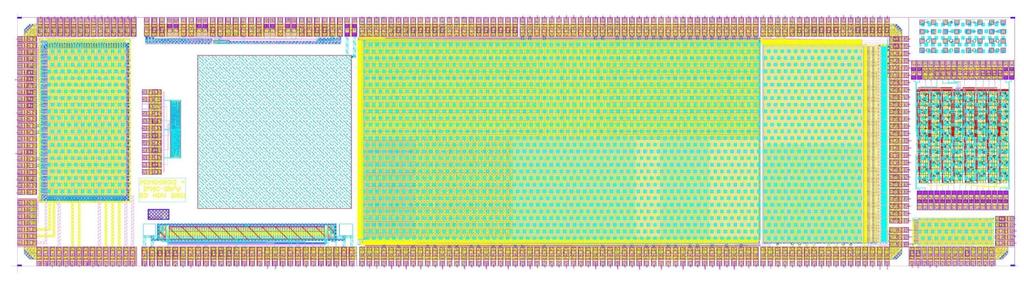
1 3.3 Discri-per-pix 80x25 array 16x80 µm JTAG structure SPAD Mimosa32: Tower CIS October 2011 submission: 4 Metal, MiM Capacitor, Quadruple Well (deep-n and deep-p wells), HR epi - Overall chip dimension: 3.3x13 = 43 mm 2 - Diodes&lifiers: 22 SF blocs for charge collection tests, 10 ampli blocs (block: 64rows x 16 columns), NMOS and PMOS based structures - Discriminators (two variety) equipped with 64 rows of pixels (4 variety of ampli?) - Novel discri-in-pixel structure ( frame readout time <10 µs) - Small blocs (LVDS I/O), novel ampli-shaper (AD-ts) - SPAD: CMOS SiPMs (InESS) Ramp generator Nwell diode 2x2 mm Diodes&Ampli: charge collection and radiation hardness study Discri (+pixels) 128 columns, two variety of discri Low power LVDS I/O AD-ts 1
2 2
3 SF0 SF00 20x40 µm 1 Diode 20x40 µm 2 Diodes 20x80 µm 1 Diode 20x80 µm 2 Diodes Amp1 Amp10 SF1 SF2 SF16 Mimosa32: Diodes&Ampli area Basic block: 16 columns x 64 rows Basic pitch: 20x20 µm, except four structures (20x40 and 20x80 µm) 16 parallel analog outputs, 5 bit (static) address)to connect single block to the output bus. Basic diode size: 3x3 µm (except Deep_Nwell, half-pinned ) Integr. time 32 µs (&2 MHz) A0 A1 A15 5 bit array address A16 A17 A31 Analog_out bus (x16) 3
4 SF structures: - P1: Nwell (octo, ~10 µm 2 ), 2T_ll, ELT - P2: Nwell_1 (octo, ~10 µm 2 ), 3T_ll, ELT - P3: Nwell_2 (TOWER design, ~10 µm 2 ), 3T_ll, ELT - P4: Nwell_1 (octo, ~10 µm 2 ), 3T_ll, SF_lin - P5: Nwell_1 (octo, ~10 µm 2 ), 3T_ll, SF_lin, bias_lin - P6: Nwell_1 (octo, ~10 µm 2 ), 3T_NMOS, SF_lin, bias_lin - P7: Dnwell (sq, ~20 µm 2 ), 3T_ll, ELT - P8: Nwell_1 (octo, ~10 µm 2 ), DeepPwellSmall, 3T_ll, ELT - P9: Nwell_1 (octo, ~10 µm 2 ), DeepPwellMedium, 3T_ll, ELT - P10: Nwell_1 (octo, ~10 µm 2 ), DeepPwellLarge, 3T_ll, ELT - P11: Half_Pinned (~9 µm 2 ), 3T_ll, ELT - P12: Half_Pinned+Nwell (9 µm 2 ), 3T_ll, ELT - P13: Nwell_gated(3x3 µm), 3T_ELT_reset_ll P14: Nwell_3.3 (octo, ~10 µm 2 ), 2T_ll, ELT - P15: Half_Pinned (sq, ~15 µm 2 ), 3T_ll, ELT - P16: Half_Pinned+Nwell (sq, ~15 µm 2 ), 3T_ll, ELT - P0: Nwell (sq. ~9 µm 2 ), 2T_ll, ELT - P00: 32xNwell + 32xNwell_NS (sq. ~9 µm 2 ), 3T_ll, ELT - Pitch 20x40 µm, 1diode - Pitch 20x40 µm, 2diodes - Pitch 20x80 µm, 1diode - Pitch 20x80 µm, 2diodes Ampli structures (preliminary): - AD_ncmos - AD_ncmos_FELT - AD_nmos - AD_nmos_FELT - AD_pcmos - AD_pmos - YD_nmos2 - YD_nmos3 - YD_pmos_4 - YD_pmos_5 4
5 Diodes&Ampli area: SF pixels - 3T readout (2T like readout) - 2T readout Vdiode (Vclamp) Vdda Vdiode (Vclamp) Vdda Reset (or LineReset) plus Global Reset Pixel SF-3T Pixel SF-2T Pixel Array Periphery Gnd Select (or LineSelect) Gnd Select (or LineSelect) Iref Out (or ColumnOut) Iref Out (or ColumnOut) Gnd Gnd 5
6 Diodes&Ampli area: clamping pixels (amplifiers) Vclamp Vdda Clamp (LineClamp) Clamping Pixel CS Amplifier PowerOn (LinePowerOn) Pixel Array Periphery Gnd Select (or LineSelect) Iref Out (or ColumnOut) Gnd 6
7 Sync Clock In Mimosa32: SF pixel array steering (clock frequency : 2 MHz) Sync Clock In Reset, Clamp PowerOn PowerOn LSelect LReset, LClamp LSelect GReset Individual Pixel Array: 16 columns x 64 rows (lines) Out 64 bit Shift Register: two hot bits Out 64 bit Shift Register: one hot bit Analog_out bus (x16) 7
8 SF pixel array steering (clock frequency : 2 MHz) Self-bias mode (Grst=1, Lrst=0): 3T reset transistors in diode setting (permanently on ) Integration time (64 clok pules) First row Last row First row, next frame Clock Sync Out In Out may be shorted to In on the PCB
9 SF pixel array steering (clock frequency : <2 MHz) Line-reset mode (Grst=0,): 3T reset transistors activated during line addressing by Lrst pulse. Integration time (64 clok pules) First row Last row First row, next frame Clock Sync Example of CDS implementation using Lrst function Signal = Frame2-Frame1, Frame5-Frame4 etc. Frame «0» Frame «1» Frame «2» Frame «3» Frame «4» Frame «5» Lrst 9
10 Discriminators area 128 columns x 64 rows Two varieties of discri, four pixels types Basic pitch: 20x20 µm 16 parallel digital outputs 3 bit (static) address to connect single block to the output bus Integration time: down to 10 µs Ampli1 Ampli2 Ampli3 Ampli4 DsA DsB DsA DsB DsA DsB DsA DsB Digital_Out (x16) 10
11 Sync Clock In Mimosa32: Ampli pixel array & discriminator steering (clock frequency : 100/16 MHz) Sync Clock In Reset, Clamp PowerOn PowerOn LSelect LReset, LClamp LSelect Individual Pixel Array: 16 columns x 64 rows (lines) Out Out Read, Calib, Latch 16 Column Discriminators 64 bit Shift Register: two hot bits 64 bit Shift Register: one hot bit Digital_out bus (x16) 11
12 Pixel (Ampli&Discri) array steering (clock frequency : 100/16 = 6.25 MHz) Integration time (64 clok pules) First row Last row First row, next frame Clock Sync Out (Pout) In (Pin) Out (Pout) may be shorted to In (Pin) on the PCB 12
13 Sensor steering signals: Ampli+Discri example Sequence corresponding to one (array) Clock Cycle (derived from 16 pulses of 100 MHz master clock) f CK =100 MHz PWRON Sel_Pix Clamp RD ( 1) Version 1 CALIB ( 2) LATCH 160 ns f CK =100 MHz PWRON Sel_Pix Clamp RD ( 1) Version 2 CALIB ( 2) LATCH 160 ns

 DAQ")
14 Sensor steering signals Power Analog Ref Array Address: static Digital Inputs Outputs (A&D) DAQ sync Outputs 14
15 Reference Analog Voltage Settings Definition Typical value from simulations Dynamic Range Resolution Iref (VLN) Column load transistor bias of pixels ~50 µa µa ~5 µa Vclp Clamping voltage of pixels ~1.2 V V 50 mv Vref1 Threshold value Vref2±30 mv 0.5 mv Vref2 Threshold common mode value of ~572.5 mv mv 5 mv discris. Vclp_discri Clamping voltage of discriminators ~975 mv mv 25 mv Vb1 Discriminators gain stage bias ~481.5 mv (to give 10 µa) mv 10 mv Vb2 Discriminators buffer stage bias ~438.5 mv (to give 5 µa) mv 10 mv All Analog Voltage Settings controlled by I 2 C DACs (or manual potentiometers) on AuxPCBs In addition: Vref (analog buffers baseline on ProxPCB_A, V) and Vcommon (Common Baseline Voltage on AuxPCB_A, only manual setting ~0V) 15
16 Annexe 16

17 Design status: back from fabrication! Tests preparation in progress 17
18 DAQ_ANALOG Mimosa32: Test PCB s design concept DAQ_DIGITAL DAQ_D DAQ_A CLK_A MK_SYNC_A 18
19 M32 tests goals ENC - Charge collection efficiency - Leakage current - Noise ENC -. - Irradiations (ionizing dose and equivalent neutron flux) -. - Tracking performance (S/N, efficiency, spatial resolution) M32 tests procedure - Correlated double sampling (digital or analog): NO diode reset between two consecutive frame readouts) - Signal = Frame2 Frame1-55 Fe photon spectrum (5.9 kev 1640 electrons): seed pixel, clustersation 55 Fe Spectrum example (M18) 19
A pixel chip for tracking in ALICE and particle identification in LHCb
 A pixel chip for tracking in ALICE and particle identification in LHCb K.Wyllie 1), M.Burns 1), M.Campbell 1), E.Cantatore 1), V.Cencelli 2) R.Dinapoli 3), F.Formenti 1), T.Grassi 1), E.Heijne 1), P.Jarron
ILC requirements Review on CMOS Performances: state of the art Progress on fast read-out sensors & ADC Roadmap for the coming years Summary
 Status on CMOS sensors Auguste Besson on behalf of DAPNIA/Saclay, LPSC/Grenoble, LPC/Clermont-F., DESY, Uni. Hamburg, JINR-Dubna & IPHC/Strasbourg contributions from IPN/Lyon, Uni. Frankfurt, GSI-Darmstadt,
PICOSECOND TIMING USING FAST ANALOG SAMPLING
 PICOSECOND TIMING USING FAST ANALOG SAMPLING H. Frisch, J-F Genat, F. Tang, EFI Chicago, Tuesday 6 th Nov 2007 INTRODUCTION In the context of picosecond timing, analog detector pulse sampling in the 10
The Alice Silicon Pixel Detector (SPD) Peter Chochula for the Alice Pixel Collaboration
 Peter Chochula for the Alice Pixel Collaboration") The Alice Silicon Pixel Detector (SPD) Peter Chochula for the Alice Pixel Collaboration The Alice Pixel Detector R 1 =3.9 cm R 2 =7.6 cm Main Physics Goal Heavy Flavour Physics D 0 K π+ 15 days Pb-Pb data
The Alice Silicon Pixel Detector (SPD) Peter Chochula for the Alice Pixel Collaboration The Alice Pixel Detector R 1 =3.9 cm R 2 =7.6 cm Main Physics Goal Heavy Flavour Physics D 0 K π+ 15 days Pb-Pb data
The ATLAS Pixel Chip FEI in 0.25µm Technology
 The ATLAS Pixel Chip FEI in 0.25µm Technology Peter Fischer, Universität Bonn (for Ivan Peric) for the ATLAS pixel collaboration The ATLAS Pixel Chip FEI Short Introduction to ATLAS Pixel mechanics, modules
Photodiode Detector with Signal Amplification
 107 Bonaventura Dr., San Jose, CA 95134 Tel: +1 408 432 9888 Fax: +1 408 432 9889 www.x-scanimaging.com Linear X-Ray Photodiode Detector Array with Signal Amplification XB8801R Series An X-Scan Imaging
A High-Speed CMOS Image Sensor with Column-Parallel Single Capacitor CDSs and Single-slope ADCs
 A High-Speed CMOS Image Sensor with Column-Parallel Single Capacitor CDSs and Single-slope ADCs LI Quanliang, SHI Cong, and WU Nanjian (The State Key Laboratory for Superlattices and Microstructures, Institute
DEPFET Active Pixel Sensors for the ILC
 DEPFET Active Pixel Sensors for the ILC Laci Andricek for the DEPFET Collaboration (www.depfet.org) The DEPFET ILC VTX Project steering chips Switcher thinning technology Simulation sensor development
ISC0904: 1k x 1k 18µm N-on-P ROIC. Specification January 13, 2012
 ISC0904 1k x 1k 18µm N-on-P ROIC Specification January 13, 2012 This presentation contains content that is proprietary to FLIR Systems. Information is subject to change without notice. 1 Version 1.00 January
RX40_V1_0 Measurement Report F.Faccio
 RX40_V1_0 Measurement Report F.Faccio This document follows the previous report An 80Mbit/s Optical Receiver for the CMS digital optical link, dating back to January 2000 and concerning the first prototype
Monolithic Thin Pixel Upgrade Testing Update. Gary S. Varner, Marlon Barbero and Fang Fang UH Belle Meeting, April 16 th 2004
 Monolithic Thin Pixel Upgrade Testing Update Gary S. Varner, Marlon Barbero and Fang Fang UH Belle Meeting, April 16 th 2004 Basic Technology: Standard CMOS CMOS Camera Because of large Capacitance, need
V6118 EM MICROELECTRONIC - MARIN SA. 2, 4 and 8 Mutiplex LCD Driver
 EM MICROELECTRONIC - MARIN SA 2, 4 and 8 Mutiplex LCD Driver Description The is a universal low multiplex LCD driver. The version 2 drives two ways multiplex (two blackplanes) LCD, the version 4, four
Status of readout electronic design in MOST1
 Status of readout electronic design in MOST1 Na WANG, Ke WANG, Zhenan LIU, Jia TAO On behalf of the Trigger Group (IHEP) Mini-workshop for CEPC MOST silicon project,23 November,2017,Beijing Outline Introduction
The hybrid photon detectors for the LHCb-RICH counters
 7 th International Conference on Advanced Technology and Particle Physics The hybrid photon detectors for the LHCb-RICH counters Maria Girone, CERN and Imperial College on behalf of the LHCb-RICH group
Conceps and trends for Front-end chips in Astroparticle physics
 Conceps and trends for Front-end chips in Astroparticle physics Eric Delagnes Fabrice Feinstein CEA/DAPNIA Saclay LPTA/IN2P3 Montpellier General interest performances Fast pulses : bandwidth > ~ 300 MHz
Front End Electronics
 CLAS12 Ring Imaging Cherenkov (RICH) Detector Mid-term Review Front End Electronics INFN - Ferrara Matteo Turisini 2015 October 13 th Overview Readout requirements Hardware design Electronics boards Integration
R&D on SOI Counting Pixel Chips
 KEK Seminar 28 January 2015 Tsukuba R&D on SOI Counting Pixel Chips Yunpeng Lu Institute of High Energy Physics(IHEP) Beijing, CHINA E-mail: yplu@ihep.ac.cn JUNO Exp. 20K ton liquid scint. 3% energy resolution(at
CCD Element Linear Image Sensor CCD Element Line Scan Image Sensor
 1024-Element Linear Image Sensor CCD 134 1024-Element Line Scan Image Sensor FEATURES 1024 x 1 photosite array 13µm x 13µm photosites on 13µm pitch Anti-blooming and integration control Enhanced spectral
Front End Electronics
 CLAS12 Ring Imaging Cherenkov (RICH) Detector Mid-term Review Front End Electronics INFN - Ferrara Matteo Turisini 2015 October 13 th Overview Readout requirements Hardware design Electronics boards Integration
A FOUR GAIN READOUT INTEGRATED CIRCUIT : FRIC 96_1
 A FOUR GAIN READOUT INTEGRATED CIRCUIT : FRIC 96_1 J. M. Bussat 1, G. Bohner 1, O. Rossetto 2, D. Dzahini 2, J. Lecoq 1, J. Pouxe 2, J. Colas 1, (1) L. A. P. P. Annecy-le-vieux, France (2) I. S. N. Grenoble,
Solid State Photon-Counters
 Solid State Photon-Counters GMAPD (Geiger Mode Avalanche PhotoDiode) SiPM (Silicon Photo-Multiplier) Single element Photon Counter Multi Pixel Photon Counter 1-cell n-cells charge = k charge = nk Giovanni
MIMOSA26 User Manual
 User Manual (Preliminary version) Institut Pluridisciplinaire Hubert Curien IN2P3-CNRS / UdS Strasbourg France CEA Saclay DAPNIA/SEDI March 2011 MIMOSA26 User Manual V.1.5 1 Document history Version Date
CCD 143A 2048-Element High Speed Linear Image Sensor
 A CCD 143A 2048-Element High Speed Linear Image Sensor FEATURES 2048 x 1 photosite array 13µm x 13µm photosites on 13µm pitch High speed = up to 20MHz data rates Enhanced spectral response Low dark signal
FRONT-END AND READ-OUT ELECTRONICS FOR THE NUMEN FPD
 FRONT-END AND READ-OUT ELECTRONICS FOR THE NUMEN FPD D. LO PRESTI D. BONANNO, F. LONGHITANO, D. BONGIOVANNI, S. REITO INFN- SEZIONE DI CATANIA D. Lo Presti, NUMEN2015 LNS, 1-2 December 2015 1 OVERVIEW
ADVANCE INFORMATION TC PIXEL CCD IMAGE SENSOR. description
 Very High-Resolution, 1/3-in Solid-State Image Sensor for NTSC Color Applications 340,000 Pixels per Field Frame Memory 658 (H) 496 (V) Active Elements in Image-Sensing Area Compatible With Electronic
Near infrared image sensor (0.9 to 1.7 µm) with high-speed data rate
 with high-speed data rate") IMAGE SENSOR InGaAs linear image sensor G99-56D/-5D Near infrared image sensor (.9 to.7 µm) with high-speed data rate HAMAMATSU provides high-speed, near infrared image sensors designed for detectors used
IMAGE SENSOR InGaAs linear image sensor G99-56D/-5D Near infrared image sensor (.9 to.7 µm) with high-speed data rate HAMAMATSU provides high-speed, near infrared image sensors designed for detectors used
Readout techniques for drift and low frequency noise rejection in infrared arrays
 Readout techniques for drift and low frequency noise rejection in infrared arrays European Southern Observatory Finger, G., Dorn, R.J, Hoffman, A.W., Mehrgan, H., Meyer, M., Moorwood, A.F.M., Stegmeier,
Atlas Pixel Replacement/Upgrade. Measurements on 3D sensors
 Atlas Pixel Replacement/Upgrade and Measurements on 3D sensors Forskerskole 2007 by E. Bolle erlend.bolle@fys.uio.no Outline Sensors for Atlas pixel b-layer replacement/upgrade UiO activities CERN 3D test
Report on 4-bit Counter design Report- 1, 2. Report on D- Flipflop. Course project for ECE533
 Report on 4-bit Counter design Report- 1, 2. Report on D- Flipflop Course project for ECE533 I. Objective: REPORT-I The objective of this project is to design a 4-bit counter and implement it into a chip
Artisan Technology Group is your source for quality new and certified-used/pre-owned equipment
 Artisan Technology Group is your source for quality new and certified-used/pre-owned equipment FAST SHIPPING AND DELIVERY TENS OF THOUSANDS OF IN-STOCK ITEMS EQUIPMENT DEMOS HUNDREDS OF MANUFACTURERS SUPPORTED
Multi-project Sensor Chip Design Global Pad Placement
 Institute of Integrated Sensor Systems Dept. of Eletrical Engineering and Information Technology Multi-project Sensor Chip Design Global Pad Placement Jiawei Yang February, 2009 Prof. Dr.-Ing. Andreas
The Readout Architecture of the ATLAS Pixel System
 The Readout Architecture of the ATLAS Pixel System Roberto Beccherle / INFN - Genova E-mail: Roberto.Beccherle@ge.infn.it Copy of This Talk: http://www.ge.infn.it/atlas/electronics/home.html R. Beccherle
The FEL detector development program at DESY. Heinz Graafsma DESY-Photon Science Detector Group WorkPackage Detectors for XFEL
 The FEL detector development program at DESY DESY-Photon Science Detector Group WorkPackage Detectors for XFEL EUROFEL-2009 Hard X-ray SASE Free Electron Lasers LINAC COHERENT LIGHT SOURCE LCLS 2009 2010
CCD220 Back Illuminated L3Vision Sensor Electron Multiplying Adaptive Optics CCD
 CCD220 Back Illuminated L3Vision Sensor Electron Multiplying Adaptive Optics CCD FEATURES 240 x 240 pixel image area 24 µm square pixels Split frame transfer 100% fill factor Back-illuminated for high
25.5 A Zero-Crossing Based 8b, 200MS/s Pipelined ADC
 25.5 A Zero-Crossing Based 8b, 200MS/s Pipelined ADC Lane Brooks and Hae-Seung Lee Massachusetts Institute of Technology 1 Outline Motivation Review of Op-amp & Comparator-Based Circuits Introduction of
Reading a GEM with a VLSI pixel ASIC used as a direct charge collecting anode. R.Bellazzini - INFN Pisa. Vienna February
 Reading a GEM with a VLSI pixel ASIC used as a direct charge collecting anode Ronaldo Bellazzini INFN Pisa Vienna February 16-21 2004 The GEM amplifier The most interesting feature of the Gas Electron
TG 3 Status Report. C. Cattadori on behalf of TG3
 TG 3 Status Report C. Cattadori on behalf of TG3 Status of FE circuits T [ns] Range[MeV] ENC rms [e-] R with crystal [kev] Output F-CSA104 Fully integrated 20 ns 0-11 MeV 270 @ LN (20 µs) 310 @ 20 C 5.4
Progress on the development of a detector mounted analog and digital readout system
 Progress on the development of a detector mounted analog and digital readout system for the ATLAS TRT Curt Baxter, Thurston Chandler, Nandor Dressnandt, Colin Gay, Bjorn Lundberg, Antoni Munar, Godwin
Performance of a double-metal n-on-n and a Czochralski silicon strip detector read out at LHC speeds
 Performance of a double-metal n-on-n and a Czochralski silicon strip detector read out at LHC speeds Juan Palacios, On behalf of the LHCb VELO group J.P. Palacios, Liverpool Outline LHCb and VELO performance
ZR x1032 Digital Image Sensor
 Description Features The PixelCam is a high-performance CMOS image sensor for digital still and video camera products. With its Distributed-Pixel Amplifier design the pixel response is independent of its
InGaAs linear image sensors
 Near infrared image sensor (0.9 to 1.7 μm) with 1024 pixels and high-speed line rate The is a 1024-channel, high-speed infrared image sensor designed for applications such as foreign object screening and
PIXEL2000, June 5-8, FRANCO MEDDI CERN-ALICE / University of Rome & INFN, Italy. For the ALICE Collaboration
 PIXEL2000, June 5-8, 2000 FRANCO MEDDI CERN-ALICE / University of Rome & INFN, Italy For the ALICE Collaboration CONTENTS: Introduction: Physics Requirements Design Considerations Present development status
Total Ionizing Dose Test Report. No. 14T-RTSX32SU-CQ256-D1RH41
 Total Ionizing Dose Test Report No. 14T-RTSX32SU-CQ256-D1RH41 March 9, 2014 Table of Contents I. Summary Table... 3 II. Total Ionizing Dose (TID) Testing... 3 A. Device-Under-Test (DUT) and Irradiation
Quadruple, 2:1, Mux Amplifiers for Standard-Definition and VGA Signals
 9-4457; Rev ; 2/9 Quadruple, 2:, Mux Amplifiers for General Description The MAX954/MAX9542 are quadruple-channel, 2: video mux amplifiers with input sync tip clamps. These devices select between two video
FMS3810/3815 Triple Video D/A Converters 3 x 8 bit, 150 Ms/s
 Triple Video D/A Converters 3 x 8 bit, 150 Ms/s Features 8-bit resolution 150 megapixels per second 0.2% linearity error Sync and blank controls 1.0V p-p video into 37.5Ω or 75Ω load Internal bandgap voltage
HAPD and Electronics Updates
 S. Nishida KEK 3rd Open Meeting for Belle II Collaboration 1 Contents Frontend Electronics Neutron Irradiation News from Hamamtsu 2 144ch HAPD HAPD (Hybrid Avalanche Photo Detector) photon bi alkali photocathode
Sensors for the CMS High Granularity Calorimeter
 Sensors for the CMS High Granularity Calorimeter Andreas Alexander Maier (CERN) on behalf of the CMS Collaboration Wed, March 1, 2017 The CMS HGCAL project ECAL Answer to HL-LHC challenges: Pile-up: up
Reading an Image using CMOS Linear Image Sensor. S.R.Shinthu 1, P.Maheswari 2, C.S.Manikandababu 3. 1 Introduction. A.
 International Journal of Inventions in Computer Science and Engineering, Volume 2 Issue 4 April 2015 Reading an Image using CMOS Linear Image Sensor S.R.Shinthu 1, P.Maheswari 2, C.S.Manikandababu 3 1,2
ECAL LED system update. A. Celentano
 ECAL LED system update A. Celentano 1 ECAL LMS overview (x 4) Design: individual bi-color LEDs mounted in front of each PbWO4 crystal. Main controllers (2 x) Driver Boards (8 x) Connection boards (4 x)
Complete 14-Bit, 56 MSPS Imaging Signal Processor AD9941
 Complete 14-Bit, 56 MSPS Imaging Signal Processor AD9941 FEATURES Differential sensor input with 1 V p-p input range 0 db/6 db variable gain amplifier (VGA) Low noise optical black clamp circuit 14-bit,
Note 5. Digital Electronic Devices
 Note 5 Digital Electronic Devices Department of Mechanical Engineering, University Of Saskatchewan, 57 Campus Drive, Saskatoon, SK S7N 5A9, Canada 1 1. Binary and Hexadecimal Numbers Digital systems perform
Chrontel CH7015 SDTV / HDTV Encoder
 Chrontel Preliminary Brief Datasheet Chrontel SDTV / HDTV Encoder Features 1.0 GENERAL DESCRIPTION VGA to SDTV conversion supporting graphics resolutions up to 104x768 Analog YPrPb or YCrCb outputs for
MM5452/MM5453 Liquid Crystal Display Drivers
 Liquid Crystal Display Drivers General Description The MM5452 is a monolithic integrated circuit utilizing CMOS metal gate, low threshold enhancement mode devices. It is available in a 40-pin molded package.
THE ATLAS Inner Detector [2] is designed for precision
![THE ATLAS Inner Detector [2] is designed for precision](/thumbs/79/79327554.jpg "THE ATLAS Inner Detector [2] is designed for precision") The ATLAS Pixel Detector Fabian Hügging on behalf of the ATLAS Pixel Collaboration [1] arxiv:physics/412138v1 [physics.ins-det] 21 Dec 4 Abstract The ATLAS Pixel Detector is the innermost layer of the
The ATLAS Pixel Detector Fabian Hügging on behalf of the ATLAS Pixel Collaboration [1] arxiv:physics/412138v1 [physics.ins-det] 21 Dec 4 Abstract The ATLAS Pixel Detector is the innermost layer of the
Development of Ultra-High-Density (UHD) Silicon Photomultipliers with improved Detection Efficiency
 Silicon Photomultipliers with improved Detection Efficiency") Development of Ultra-High-Density (UHD) Silicon Photomultipliers with improved Detection Efficiency Fabio Acerbi, Alberto Gola, Giovanni Paternoster, Claudio Piemonte, Nicola Zorzi http://iris.fbk.eu/silicon-photomultipliers
Development of Ultra-High-Density (UHD) Silicon Photomultipliers with improved Detection Efficiency Fabio Acerbi, Alberto Gola, Giovanni Paternoster, Claudio Piemonte, Nicola Zorzi http://iris.fbk.eu/silicon-photomultipliers
The Read-Out system of the ALICE pixel detector
 The Read-Out system of the ALICE pixel detector Kluge, A. for the ALICE SPD collaboration CERN, CH-1211 Geneva 23, Switzerland Abstract The on-detector electronics of the ALICE silicon pixel detector (nearly
The Readout Architecture of the ATLAS Pixel System. 2 The ATLAS Pixel Detector System
 The Readout Architecture of the ATLAS Pixel System Roberto Beccherle, on behalf of the ATLAS Pixel Collaboration Istituto Nazionale di Fisica Nucleare, Sez. di Genova Via Dodecaneso 33, I-646 Genova, ITALY
nc... Freescale Semiconductor, I
 Application Note Rev. 0, 2/2003 Interfacing to the HCS12 ATD Module by Martyn Gallop, Application Engineering, Freescale, East Kilbride Introduction Many of the HCS12 family of 16-bit microcontrollers
S6B CH SEGMENT DRIVER FOR DOT MATRIX LCD
 64 CH SEGMENT DRIVER FOR DOT MATRIX LCD June. 2000. Ver. 0.0 Contents in this document are subject to change without notice. No part of this document may be reproduced or transmitted in any form or by
VLSI Design: 3) Explain the various MOSFET Capacitances & their significance. 4) Draw a CMOS Inverter. Explain its transfer characteristics
 Explain the various MOSFET Capacitances & their significance. 4) Draw a CMOS Inverter. Explain its transfer characteristics") 1) Explain why & how a MOSFET works VLSI Design: 2) Draw Vds-Ids curve for a MOSFET. Now, show how this curve changes (a) with increasing Vgs (b) with increasing transistor width (c) considering Channel
1) Explain why & how a MOSFET works VLSI Design: 2) Draw Vds-Ids curve for a MOSFET. Now, show how this curve changes (a) with increasing Vgs (b) with increasing transistor width (c) considering Channel
64CH SEGMENT DRIVER FOR DOT MATRIX LCD
 64CH SEGMENT DRIVER FOR DOT MATRIX LCD INTRODUCTION The (TQFP type: S6B2108) is a LCD driver LSI with 64 channel output for dot matrix liquid crystal graphic display systems. This device consists of the
A TARGET-based camera for CTA
 A TARGET-based camera for CTA TeV Array Readout with GSa/s sampling and Event Trigger (TARGET) chip: overview Custom-designed ASIC for CTA, developed in collaboration with Gary Varner (U Hawaii) Implementation:
A new Scintillating Fibre Tracker for LHCb experiment
 A new Scintillating Fibre Tracker for LHCb experiment Alexander Malinin, NRC Kurchatov Institute on behalf of the LHCb-SciFi-Collaboration Instrumentation for Colliding Beam Physics BINP, Novosibirsk,
HARDROC, Readout chip of the Digital Hadronic Calorimeter of ILC
 HARDROC, Readout chip of the Digital Hadronic Calorimeter of ILC S. Callier a, F. Dulucq a, C. de La Taille a, G. Martin-Chassard a, N. Seguin-Moreau a a OMEGA/LAL/IN2P3, LAL Université Paris-Sud, Orsay,France
The Silicon Pixel Detector (SPD) for the ALICE Experiment
 for the ALICE Experiment") The Silicon Pixel Detector (SPD) for the ALICE Experiment V. Manzari/INFN Bari, Italy for the SPD Project in the ALICE Experiment INFN and Università Bari, Comenius University Bratislava, INFN and Università
The Silicon Pixel Detector (SPD) for the ALICE Experiment V. Manzari/INFN Bari, Italy for the SPD Project in the ALICE Experiment INFN and Università Bari, Comenius University Bratislava, INFN and Università
CCD Datasheet Electron Multiplying CCD Sensor Back Illuminated, 1024 x 1024 Pixels 2-Phase IMO
 CCD351-00 Datasheet Electron Multiplying CCD Sensor Back Illuminated, 1024 x 1024 Pixels 2-Phase IMO MAIN FEATURES 1024 x 1024 active pixels 10µm square pixels Variable multiplicative gain Frame rates
Flip-Flops A) Synchronization: Clocks and Latches B) Two Stage Latch C) Memory Requires Feedback D) Simple Flip-Flop Gate
 Synchronization: Clocks and Latches B) Two Stage Latch C) Memory Requires Feedback D) Simple Flip-Flop Gate") Lecture 19: November 5, 2001 Midterm in Class Wed. Nov 7 th Covers Material 6 th -10 th week including W#10 Closed Book, Closed Notes, Bring Calculator, Paper Provided Last Name A-K 2040 Valley LSB; Last
Lecture 19: November 5, 2001 Midterm in Class Wed. Nov 7 th Covers Material 6 th -10 th week including W#10 Closed Book, Closed Notes, Bring Calculator, Paper Provided Last Name A-K 2040 Valley LSB; Last
The ATLAS Pixel Detector
 The ATLAS Pixel Detector Fabian Hügging arxiv:physics/0412138v2 [physics.ins-det] 5 Aug 5 Abstract The ATLAS Pixel Detector is the innermost layer of the ATLAS tracking system and will contribute significantly
110 MHz 256-Word Color Palette 15-, 16-, and 24-Bit True Color Power-Down RAMDAC
 110 MHz 256-Word Color Palette 15-, 16-, and 24-Bit True Color Power-Down RAMDAC Designed specifically for high-performance color graphics, the RAM- DAC supports three true-color modes: 15-bit (5:5:5,
DATASHEET EL1883. Features. Applications. Ordering Information. Demo Board. Pinout. Sync Separator with Horizontal Output. FN7010 Rev 2.
 DATASHEET EL883 Sync Separator with Horizontal Output FN7 Rev 2. The EL883 video sync separator is manufactured using Elantec s high performance analog CMOS process. This device extracts sync timing information
CAEN Tools for Discovery
 Viareggio March 28, 2011 Introduction: what is the SiPM? The Silicon PhotoMultiplier (SiPM) consists of a high density (up to ~10 3 /mm 2 ) matrix of diodes connected in parallel on a common Si substrate.
TMC3503 Triple Video D/A Converter 8 bit, 80 Msps, 5V
 Triple Video D/A Converter 8 bit, 80 Msps, 5V Features 8-bit resolution 80, 50, and 30 megapixels per second ±0.5 LSB linearity error Sync, blank, and white controls Independent sync current output 1.0V
OBSOLETE. CMOS 80 MHz Monolithic (18) Color Palette RAM-DACs ADV478/ADV471
 Color Palette RAM-DACs ADV478/ADV471") a FEATURES Personal System/2* Compatible 80 MHz Pipelined Operation Triple 8-Bit (6-Bit) D/A Converters 256 24(18) Color Palette RAM 15 24(18) Overlay Registers RS-343A/RS-170 Compatible Outputs Sync on
a FEATURES Personal System/2* Compatible 80 MHz Pipelined Operation Triple 8-Bit (6-Bit) D/A Converters 256 24(18) Color Palette RAM 15 24(18) Overlay Registers RS-343A/RS-170 Compatible Outputs Sync on
Design and Simulation of a Digital CMOS Synchronous 4-bit Up-Counter with Set and Reset
 Design and Simulation of a Digital CMOS Synchronous 4-bit Up-Counter with Set and Reset Course Number: ECE 533 Spring 2013 University of Tennessee Knoxville Instructor: Dr. Syed Kamrul Islam Prepared by
Specifications for Thermopilearrays HTPA8x8, HTPA16x16 and HTPA32x31 Rev.6: Fg
 Principal Schematic for HTPA16x16: - 1 - Pin Assignment in TO8 for 8x8: Connect all reference voltages via 100 nf capacitors to VSS. Pin Assignment 8x8 Pin Name Description Type 1 VSS Negative power supply
A Multi-Channel Time-to-Digital Converter Chip for Drift Chamber Readout
 LBL 38039 A Multi-Channel Time-to-Digital Converter Chip for Drift Chamber Readout Talk presented at the EEE Nuclear Science Symposium and Medical maging Conference October 1995 Dinis M. Santos Aveiro
DIFFERENTIAL CONDITIONAL CAPTURING FLIP-FLOP TECHNIQUE USED FOR LOW POWER CONSUMPTION IN CLOCKING SCHEME
 DIFFERENTIAL CONDITIONAL CAPTURING FLIP-FLOP TECHNIQUE USED FOR LOW POWER CONSUMPTION IN CLOCKING SCHEME Mr.N.Vetriselvan, Assistant Professor, Dhirajlal Gandhi College of Technology Mr.P.N.Palanisamy,
Technology Scaling Issues of an I DDQ Built-In Current Sensor
 Technology Scaling Issues of an I DDQ Built-In Current Sensor Bin Xue, D. M. H. Walker Dept. of Computer Science Texas A&M University College Station TX 77843-3112 Tel: (979) 862-4387 Email: {binxue, walker}@cs.tamu.edu
IEEE TRANSACTIONS ON NUCLEAR SCIENCE, VOL. 52, NO. 5, OCTOBER
 IEEE TRANSACTIONS ON NUCLEAR SCIENCE, VOL. 52, NO. 5, OCTOBER 2005 2009 3-D Position Sensitive CdZnTe Spectrometer Performance Using Third Generation VAS/TAT Readout Electronics Feng Zhang, Zhong He, Senior
Lecture 14: Computer Peripherals
 Lecture 14: Computer Peripherals The last homework and lab for the course will involve using programmable logic to make interesting things happen on a computer monitor should be even more fun than the
High Performance TFT LCD Driver ICs for Large-Size Displays
 Name: Eugenie Ip Title: Technical Marketing Engineer Company: Solomon Systech Limited www.solomon-systech.com The TFT LCD market has rapidly evolved in the last decade, enabling the occurrence of large
OV µm Pixel Size Back Side Illuminated (BSI) 5 Megapixel CMOS Image Sensor
 5 Megapixel CMOS Image Sensor") OmniVision OV5642 1.4 µm Pixel Size Back Side Illuminated (BSI) 5 Megapixel CMOS Image Sensor Circuit Analysis of the Pixel Array, Row Control, Column Readout, Analog Front End, and Pipelined A/D Converter
OmniVision OV5642 1.4 µm Pixel Size Back Side Illuminated (BSI) 5 Megapixel CMOS Image Sensor Circuit Analysis of the Pixel Array, Row Control, Column Readout, Analog Front End, and Pipelined A/D Converter
FE-I4B wafer probing. ATLAS IBL General Meeting February David-Leon Pohl, Malte Backhaus, Marlon Barbero, Jörn Große-Knetter.
 FE-I4B wafer probing ATLAS IBL General Meeting February 15-17 2012 1 of 16 FE-I4A wafer probing summary 20 FE-I4A wafers fully probed (80% Bonn, 20% Berkeley) 2 unprobed wafers for diced chips 4 at Aptasic
NT Output LCD Segment/Common Driver NT7701. Features. General Description. Pin Configuration 1 V1.0
 160 Output LCD Segment/Common Driver Features (Segment mode)! Shift Clock frequency : 14 MHz (Max.) (VDD = 5V ± 10%) 8 MHz (Max.) (VDD = 2.5V - 4.5V)! Adopts a data bus system! 4-bit/8-bit parallel input
High ResolutionCross Strip Anodes for Photon Counting detectors
 High ResolutionCross Strip Anodes for Photon Counting detectors Oswald H.W. Siegmund, Anton S. Tremsin, Robert Abiad, J. Hull and John V. Vallerga Space Sciences Laboratory University of California Berkeley,
PERFORMANCE ANALYSIS OF AN EFFICIENT TIME-TO-THRESHOLD PWM ARCHIECTURE USING CMOS TECHNOLOGY
 PERFORMANCE ANALYSIS OF AN EFFICIENT TIME-TO-THRESHOLD PWM ARCHIECTURE USING CMOS TECHNOLOGY T. Jaya Bharathi and N. Mathan VLSI Design, Department of Electronics and Communication Engineering, Sathyabama
MUHAMMAD NAEEM LATIF MCS 3 RD SEMESTER KHANEWAL
 1. A stage in a shift register consists of (a) a latch (b) a flip-flop (c) a byte of storage (d) from bits of storage 2. To serially shift a byte of data into a shift register, there must be (a) one click
ROM MEMORY AND DECODERS
 ROM MEMORY AND DECODERS INEL427 - Spring 22 RANDOM ACCESS MEMORY Random Access Memory (RAM) read and write memory volatile Static RAM (SRAM) store information as long as power is applied will not lose
HT9B92 RAM Mapping 36 4 LCD Driver
 RAM Mapping 36 4 LCD Driver Feature Logic Operating Voltage: 2.4V~5.5V Integrated oscillator circuitry Bias: 1/2 or 1/3; Duty: 1/4 Internal LCD bias generation with voltage-follower buffers External pin
M66004SP/FP M66004SP/FP MITSUBISHI DIGITAL ASSP ASSP 16-DIGIT 5X7-SEGMENT VFD CONTROLLER 16-DIGIT 5 7-SEGMENT VFD CONTROLLER
 ASSP M664SP/FP M664SP/FP 6-DIGIT 5X7-SEGMENT FD CONTROLLER 6-DIGIT 5 7-SEGMENT FD CONTROLLER DESCRIPTION The M664 is a 6-digit 5 7-segment vacuum fluorescent display (FD) controller using the silicon gate
Report from the Tracking and Vertexing Group:
 Report from the Tracking and Vertexing Group: October 10, 2016 Sally Seidel, Petra Merkel, Maurice Garcia- Sciveres Structure of parallel session n Silicon Sensor Fabrication on 8 wafers (Ron Lipton) n
CCD Signal Processor For Electronic Cameras AD9801
 a FEATURES 10-Bit, 18 MSPS A/D Converter 18 MSPS Full-Speed CDS Low Noise, Wideband PGA Internal Voltage Reference No Missing Codes Guaranteed +3 V Single Supply Operation Low Power CMOS: 185 mw 48-Pin
LHCb and its electronics. J. Christiansen On behalf of the LHCb collaboration
 LHCb and its electronics J. Christiansen On behalf of the LHCb collaboration Physics background CP violation necessary to explain matter dominance B hadron decays good candidate to study CP violation B
THE WaveDAQ SYSTEM FOR THE MEG II UPGRADE
 Stefan Ritt, Paul Scherrer Institute, Switzerland Luca Galli, Fabio Morsani, Donato Nicolò, INFN Pisa, Italy THE WaveDAQ SYSTEM FOR THE MEG II UPGRADE DRS4 Chip 0.2-2 ns Inverter Domino ring chain IN Clock
HCF4027B DUAL J-K MASTER SLAVE FLIP-FLOP
 DUAL J-K MASTER SLAVE FLIP-FLOP SET RESET CAPABILITY STATIC FLIP-FLOP OPERATION - RETAINS STATE INDEFINETELY WITH CLOCK LEVEL EITHER HIGH OR LOW MEDIUM-SPEED OPERATION - 16MHz (Typ. clock toggle rate at
IEEE copyright notice
 This paper is a preprint (IEEE accepted status). It has been published in IEEE Xplore Proceedings for 2017 13th Conference on Ph.D. Research in Microelectronics and Electronics (PRIME) DOI: 10.1109/PRIME.2017.7974100
12-Bit Serial Daisy-Chain CMOS D/A Converter DAC8143
 a FEATURES Fast, Flexible, Microprocessor Interfacing in Serially Controlled Systems Buffered Digital Output Pin for Daisy-Chaining Multiple DACs Minimizes Address-Decoding in Multiple DAC Systems Three-Wire
Analog to Digital Conversion
 Analog to Digital Conversion What the heck is analog to digital conversion? Why do we care? Analog to Digital Conversion What the heck is analog to digital conversion? Why do we care? A means to convert
Complete 10-Bit, 25 MHz CCD Signal Processor AD9943
 a FEATURES 25 MSPS Correlated Double Sampler (CDS) 6 db to 40 db 10-Bit Variable Gain Amplifier (VGA) Low Noise Optical Black Clamp Circuit Preblanking Function 10-Bit, 25 MSPS A/D Converter No Missing
Scintillation Tile Hodoscope for the PANDA Barrel Time-Of-Flight Detector
 Scintillation Tile Hodoscope for the PANDA Barrel Time-Of-Flight Detector William Nalti, Ken Suzuki, Stefan-Meyer-Institut, ÖAW on behalf of the PANDA/Barrel-TOF(SciTil) group 12.06.2018, ICASiPM2018 1