Multi-project Sensor Chip Design Global Pad Placement
|
|
|
- Hollie Joseph
- 5 years ago
- Views:
Transcription
1 Institute of Integrated Sensor Systems Dept. of Eletrical Engineering and Information Technology Multi-project Sensor Chip Design Global Pad Placement Jiawei Yang February, 2009 Prof. Dr.-Ing. Andreas König
2 Overview 1. Introduction Task 2. Parts of the Project Global Schematic Global layout Simulation Pins Pads selection Package Pads Placement 3. Conclusion Signal pad Power pad
3 Task This global task is to place the I/O pads and global pads for the Multiproject Sensor Chip.
4 Task
5 Individual Project Project 2: Designed by Abhay Project 6: Designed by Kuan Shang Project 3: Designed by Mahesh Project 4: Designed by Jiawei Yang Project 1: Designed by Juergen Hornberger Project 5: Designed by Robert Freier Project 8: Designed by Hetteries Martin (links to the ppt of each project can be added later)
6 Global Task Placing, Routing, global simulation: Juergen Hornberger Global decoder cells Rows/columns: Abhay Analog MUX design and layout: Mahesh Placements of I/O pads and Global pads: Jiawei Yang Source follower load placements: Robert Freier Reference voltage: Kuan Shang

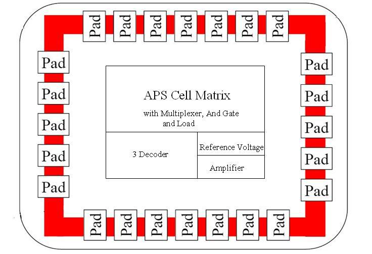
7 Global Schematic Row Decoder P2 P6 P3 P4 P1 P5 P8 Column Decoder Reference voltage Project Select Amplifier

8 Layout P2 P6 P3 P4 P1 Row Decoder Amplifier Column Decoder P5 P7 Project Decoder Reference voltage
 Column Selected by Column Address Decoder Column 2, input signal: 0001 (LSB Cbit4) VDD, Shutter, Reset: 3.3v IREF: 11.")
9 Simulation Simulation from schematic Project Selected by Project Select Decoder Project 4, input signal: 011(LSB Pbit3) Row Selected by Row Address Decoder Row 2, input signal: (LSB Rbit5) Column Selected by Column Address Decoder Column 2, input signal: 0001 (LSB Cbit4) VDD, Shutter, Reset: 3.3v IREF: 11.7uA Result
10 Simulation Result Project4

11 Simulation Result Offset voltage A( m, v)

12 Simulation Result Readout Time A( m, )

13 Simulation Result Project1

14 Simulation Result Offset voltage A(2.3m, 2.278v)

15 Simulation Result Readout Time A( m, 2.278v)
16 Result Input Output Project VDD Row Decoder Input Column Decoder Input Project Decoder Input Rest Shutter IREF Output Voltage Readout Time Project4 3.3v v 3.3v 11.7uA v 540ns Project1 3.3v v 3.3v 11.7uA 2.278v 1520ns
17 Signal pad Signal pad die placement considerations: The logic located on the die that will connect to the pad. Bonding wire angles. Cross-talk between pads. The analog pad should be as close as to the analog signal. ESD considerations charge concentrates at points, like in comers of the die pads placed in the corners of the die may be more susceptible to ESD, so use VSS pads in the die corners.
18 Power pad Power pad die placement considerations: Don't place different power rails next to each other. Power pads should be close to fast switching outputs with high slew rates, particularly if those output pads drive large loads. The ground pad of the digital device and the Analog device should be separated ( if necessary).
19 Pad Placement Strategy Counts the number of pins. Conclusion the pads number and types. Select the package according to the number of pads. Considering the shape of the package and the circuit. Considering the bonding rules. Considering the distance between the pads. Considering the whole circuit structure and path delay, in order to reduce the interconnection length and circuit delay. Minimum core/chip area consumption Pad placement
20 Pad Selection Device Pin Name Pin used Pin type Pad select Row Select Decoder Rbit 5 digital input ISP_3B Project Select Decoder Pbit 3 digital input ISP_3B Column Select Decoder Cbit 4 digital input ISP_3B Global Shutter 1 digital input ISP_3B Global RES (reset) 1 digital input ISP_3B Global vdd! 1 VDD AVDDALLP Global gnd! 1 Ground AGNDALLP Reference Voltage IREF 1 analog input APRIO200P Project5 Vmode Vconfigure Vin0 Vin1 Vin2 Vin3 Vin4 Vin5 8 digital input BBC8P_3B Project8 Output 8 digital output BBC8P_3B
21 Pad Placement The total pins are 34. Project 5 and 8 can share the 8 pins by bidirectional pads. Total pads: 26 Select DIL_28 package Pad finger: The circuit layout is rectangle Pad Placement: 4 sides, The die area: x
22 Pin and Pad Pin Name Pad Name Rbit1/Rbit2/Rbit3/Rbit4/Rbit5 Rbit1/Rbit2/Rbit3/Rbit4/Rbit5 Pbit1/Pbit2/Pbit3 Cbit1/Cbit2/Cbit3/Cbit4 Shutter RES (reset) vdd! gnd! IREF Vmode /Vconfigure /Vin0 /Vin1/Vin2 /Vin3 /Vin4 /Vin5 Output1/Output2/Output3/Output4/Out put5/output6/output7/output8 Pbit1/Pbit2/Pbit3 Cbit1/Cbit2/Cbit3/Cbit4 Shutter RES vdd! gnd! IREF IO1/IO2/IO3/IO4/IO5/IO6/IO7/IO8 IO1/IO2/IO3/IO4/IO5/IO6/IO7/IO8

23 Pad Placement Pbit2 Pbit3

24 Pad frame Pbit2 Pbit3

25 Bonding Pattern 45 degree 4.5mm

26 Layout Check The hot nwell error from project 3, others from the standard amplifier and the standard corner used in the project.
27 Conclusion The project is to place the I/O pads and global pads for the Multiproject Sensor Chip. It is no necessary in this project to separate digital ground and analog ground. In order to put the analog output as close as to the pad, reorganize the layout. Minimum the cost, project 5 and 8 share 8 bit I/O pads by using bidirectional pad.
28 Image Sensor Design Thank You for your attention!

29 Project Selection Simulation

30 Row Selection Simulation

31 Column Selection Simulation
ISC0904: 1k x 1k 18µm N-on-P ROIC. Specification January 13, 2012
 ISC0904 1k x 1k 18µm N-on-P ROIC Specification January 13, 2012 This presentation contains content that is proprietary to FLIR Systems. Information is subject to change without notice. 1 Version 1.00 January
12-bit Wallace Tree Multiplier CMPEN 411 Final Report Matthew Poremba 5/1/2009
 12-bit Wallace Tree Multiplier CMPEN 411 Final Report Matthew Poremba 5/1/2009 Project Overview This project was originally titled Fast Fourier Transform Unit, but due to space and time constraints, the
EL302 DIGITAL INTEGRATED CIRCUITS LAB #3 CMOS EDGE TRIGGERED D FLIP-FLOP. Due İLKER KALYONCU, 10043
 EL302 DIGITAL INTEGRATED CIRCUITS LAB #3 CMOS EDGE TRIGGERED D FLIP-FLOP Due 16.05. İLKER KALYONCU, 10043 1. INTRODUCTION: In this project we are going to design a CMOS positive edge triggered master-slave
Introduction to CMOS VLSI Design (E158) Lecture 11: Decoders and Delay Estimation
 Lecture 11: Decoders and Delay Estimation") Harris Introduction to CMOS VLSI Design (E158) Lecture 11: Decoders and Delay Estimation David Harris Harvey Mudd College David_Harris@hmc.edu Based on EE271 developed by Mark Horowitz, Stanford University
Harris Introduction to CMOS VLSI Design (E158) Lecture 11: Decoders and Delay Estimation David Harris Harvey Mudd College David_Harris@hmc.edu Based on EE271 developed by Mark Horowitz, Stanford University
Timing EECS141 EE141. EE141-Fall 2011 Digital Integrated Circuits. Pipelining. Administrative Stuff. Last Lecture. Latch-Based Clocking.
 EE141-Fall 2011 Digital Integrated Circuits Lecture 2 Clock, I/O Timing 1 4 Administrative Stuff Pipelining Project Phase 4 due on Monday, Nov. 21, 10am Homework 9 Due Thursday, December 1 Visit to Intel
MT8812 ISO-CMOS. 8 x 12 Analog Switch Array. Features. Description. Applications
 MT882 8 x 2 Analog Switch Array Features Internal control latches and address decoder Short set-up and hold times Wide operating voltage: 4.5V to 4.5V 4Vpp analog signal capability R ON 65 max. @ V DD
Boolean, 1s and 0s stuff: synthesis, verification, representation This is what happens in the front end of the ASIC design process
 (Lec 11) From Logic To Layout What you know... Boolean, 1s and 0s stuff: synthesis, verification, representation This is what happens in the front end of the ASIC design process High-level design description
IC Mask Design. Christopher Saint Judy Saint
 IC Mask Design Essential Layout Techniques Christopher Saint Judy Saint McGraw-Hill New York Chicago San Francisco Lisbon London Madrid Mexico City Milan New Delhi San Juan Seoul Singapore Sydney Toronto
Report on 4-bit Counter design Report- 1, 2. Report on D- Flipflop. Course project for ECE533
 Report on 4-bit Counter design Report- 1, 2. Report on D- Flipflop Course project for ECE533 I. Objective: REPORT-I The objective of this project is to design a 4-bit counter and implement it into a chip
Digital Electronics Lab #4 February 12, 2008
 Mission Overview Your mission is to help develop a Load Before Launch Sequencer (LBLS) for the USS Harry S. Truman (CVN-75). The purpose of the LBLS is to alert the Yellow Shirts (the people who flag the
Computer Systems Architecture
 Computer Systems Architecture Fundamentals Of Digital Logic 1 Our Goal Understand Fundamentals and basics Concepts How computers work at the lowest level Avoid whenever possible Complexity Implementation
A FOUR GAIN READOUT INTEGRATED CIRCUIT : FRIC 96_1
 A FOUR GAIN READOUT INTEGRATED CIRCUIT : FRIC 96_1 J. M. Bussat 1, G. Bohner 1, O. Rossetto 2, D. Dzahini 2, J. Lecoq 1, J. Pouxe 2, J. Colas 1, (1) L. A. P. P. Annecy-le-vieux, France (2) I. S. N. Grenoble,
L12: Reconfigurable Logic Architectures
 L12: Reconfigurable Logic Architectures Acknowledgements: Materials in this lecture are courtesy of the following sources and are used with permission. Frank Honore Prof. Randy Katz (Unified Microelectronics
Discussion of New Equipment
 Mission Overview Your mission is to help develop a Load Before Launch Sequencer (LBLS) for the USS Harry S. Truman (CVN-75). The purpose of the LBLS is to alert the Yellow Shirts (the people who flag the
Mimosa32: Tower CIS October 2011 submission: 4 Metal, MiM Capacitor, Quadruple Well (deep-n and deep-p wells), HR epi
, HR epi") 3.3 Discri-per-pix 80x25 array 16x80 µm JTAG structure SPAD Mimosa32: Tower CIS October 2011 submission: 4 Metal, MiM Capacitor, Quadruple Well (deep-n and deep-p wells), HR epi - Overall chip dimension:
3.3 Discri-per-pix 80x25 array 16x80 µm JTAG structure SPAD Mimosa32: Tower CIS October 2011 submission: 4 Metal, MiM Capacitor, Quadruple Well (deep-n and deep-p wells), HR epi - Overall chip dimension:
Design and Simulation of a Digital CMOS Synchronous 4-bit Up-Counter with Set and Reset
 Design and Simulation of a Digital CMOS Synchronous 4-bit Up-Counter with Set and Reset Course Number: ECE 533 Spring 2013 University of Tennessee Knoxville Instructor: Dr. Syed Kamrul Islam Prepared by
Scan. This is a sample of the first 15 pages of the Scan chapter.
 Scan This is a sample of the first 15 pages of the Scan chapter. Note: The book is NOT Pinted in color. Objectives: This section provides: An overview of Scan An introduction to Test Sequences and Test
MT8814AP. ISO-CMOS 8 x 12 Analog Switch Array. Features. -40 to 85 C. Description. Applications
 MT884 8 x 2 Analog Switch Array Features Internal control latches and address decoder Short set-up and hold times Wide operating voltage: 4.5 to 3.2 2pp analog signal capability R ON 65Ω max. @ DD =2,
MT8806 ISO-CMOS 8x4AnalogSwitchArray
 MT886 ISO-CMOS 8x4AnalogSwitchArray Features Internal control latches and address decoder Short set-up and hold times Wide operating voltage: 4.5 V to 3.2 V 2Vpp analog signal capability R ON 65 max. @
L11/12: Reconfigurable Logic Architectures
 L11/12: Reconfigurable Logic Architectures Acknowledgements: Materials in this lecture are courtesy of the following people and used with permission. - Randy H. Katz (University of California, Berkeley,
External Hardware Trigger Settings for RICOH Stereo Cameras
 External Hardware Trigger Settings for RICOH Stereo Cameras User s Guide RICOH Industrial Solutions Inc. 1/10 Contents 1. FUNCTIONAL OVERVIEW... 3 [Timing Diagram]... 3 2. POWER CONNECTOR... 4 [Connector
OFC & VLSI SIMULATION LAB MANUAL
 DEVBHOOMI INSTITUTE OF TECHNOLOGY FOR WOMEN, DEHRADUN - 24847 DEPARTMENT OF ELECTRONICS AND COMMUNICATION ENGINEERING Prepared BY: Ajay Kumar Gautam Asst. Prof. Electronics & Communication Engineering
CSE140L: Components and Design Techniques for Digital Systems Lab. CPU design and PLDs. Tajana Simunic Rosing. Source: Vahid, Katz
 CSE140L: Components and Design Techniques for Digital Systems Lab CPU design and PLDs Tajana Simunic Rosing Source: Vahid, Katz 1 Lab #3 due Lab #4 CPU design Today: CPU design - lab overview PLDs Updates
Cascadable 4-Bit Comparator
 EE 415 Project Report for Cascadable 4-Bit Comparator By William Dixon Mailbox 509 June 1, 2010 INTRODUCTION... 3 THE CASCADABLE 4-BIT COMPARATOR... 4 CONCEPT OF OPERATION... 4 LIMITATIONS... 5 POSSIBILITIES
Sitronix ST CH Segment Driver for Dot Matrix LCD. !"Dot matrix LCD driver with two 40 channel
 ST Sitronix ST7063 80CH Segment Driver for Dot Matrix LCD Functions Features!"Dot matrix LCD driver with two 40 channel outputs!"bias voltage (V1 ~ V4)!"input/output signals #"Input : Serial display data
LM16X21A Dot Matrix LCD Unit
 LCD Data Sheet FEATURES STC (Super Twisted igh Contrast) Yellow Green Transmissive Type Low Power Consumption Thin, Lightweight Design Permits Easy Installation in a Variety of Equipment General Purpose
JRC ( JTAG Route Controller ) Data Sheet
 Data Sheet") JRC ( JTAG Route Controller ) Data Sheet ATLAS TGC Electronics Group September 5, 2002 (version 1.1) Author : Takashi Takemoto Feature * JTAG signal router with two inputs and seven outputs. * Routing
JRC ( JTAG Route Controller ) Data Sheet ATLAS TGC Electronics Group September 5, 2002 (version 1.1) Author : Takashi Takemoto Feature * JTAG signal router with two inputs and seven outputs. * Routing
PICOSECOND TIMING USING FAST ANALOG SAMPLING
 PICOSECOND TIMING USING FAST ANALOG SAMPLING H. Frisch, J-F Genat, F. Tang, EFI Chicago, Tuesday 6 th Nov 2007 INTRODUCTION In the context of picosecond timing, analog detector pulse sampling in the 10
CCD220 Back Illuminated L3Vision Sensor Electron Multiplying Adaptive Optics CCD
 CCD220 Back Illuminated L3Vision Sensor Electron Multiplying Adaptive Optics CCD FEATURES 240 x 240 pixel image area 24 µm square pixels Split frame transfer 100% fill factor Back-illuminated for high
MT x 12 Analog Switch Array
 MT885 8 x 2 Analog Switch Array Features Internal control latches and address decoder Short set-up and hold times Wide operating voltage: 4.5V to 3.2V 2Vpp analog signal capability R ON 65 max. @ V DD
OV µm Pixel Size Back Side Illuminated (BSI) 5 Megapixel CMOS Image Sensor
 5 Megapixel CMOS Image Sensor") OmniVision OV5642 1.4 µm Pixel Size Back Side Illuminated (BSI) 5 Megapixel CMOS Image Sensor Circuit Analysis of the Pixel Array, Row Control, Column Readout, Analog Front End, and Pipelined A/D Converter
OmniVision OV5642 1.4 µm Pixel Size Back Side Illuminated (BSI) 5 Megapixel CMOS Image Sensor Circuit Analysis of the Pixel Array, Row Control, Column Readout, Analog Front End, and Pipelined A/D Converter
A pixel chip for tracking in ALICE and particle identification in LHCb
 A pixel chip for tracking in ALICE and particle identification in LHCb K.Wyllie 1), M.Burns 1), M.Campbell 1), E.Cantatore 1), V.Cencelli 2) R.Dinapoli 3), F.Formenti 1), T.Grassi 1), E.Heijne 1), P.Jarron
Specifications for Thermopilearrays HTPA8x8, HTPA16x16 and HTPA32x31 Rev.6: Fg
 Principal Schematic for HTPA16x16: - 1 - Pin Assignment in TO8 for 8x8: Connect all reference voltages via 100 nf capacitors to VSS. Pin Assignment 8x8 Pin Name Description Type 1 VSS Negative power supply
V6118 EM MICROELECTRONIC - MARIN SA. 2, 4 and 8 Mutiplex LCD Driver
 EM MICROELECTRONIC - MARIN SA 2, 4 and 8 Mutiplex LCD Driver Description The is a universal low multiplex LCD driver. The version 2 drives two ways multiplex (two blackplanes) LCD, the version 4, four
The Alice Silicon Pixel Detector (SPD) Peter Chochula for the Alice Pixel Collaboration
 Peter Chochula for the Alice Pixel Collaboration") The Alice Silicon Pixel Detector (SPD) Peter Chochula for the Alice Pixel Collaboration The Alice Pixel Detector R 1 =3.9 cm R 2 =7.6 cm Main Physics Goal Heavy Flavour Physics D 0 K π+ 15 days Pb-Pb data
The Alice Silicon Pixel Detector (SPD) Peter Chochula for the Alice Pixel Collaboration The Alice Pixel Detector R 1 =3.9 cm R 2 =7.6 cm Main Physics Goal Heavy Flavour Physics D 0 K π+ 15 days Pb-Pb data
64CH SEGMENT DRIVER FOR DOT MATRIX LCD
 64CH SEGMENT DRIVER FOR DOT MATRIX LCD INTRODUCTION The (TQFP type: S6B2108) is a LCD driver LSI with 64 channel output for dot matrix liquid crystal graphic display systems. This device consists of the
CS/EE 6710 Digital VLSI Design CAD Assignment #3 Due Thursday September 21 st, 5:00pm
 CS/EE 6710 Digital VLSI Design CAD Assignment #3 Due Thursday September 21 st, 5:00pm Overview: In this assignment you will design a register cell. This cell should be a single-bit edge-triggered D-type
NT Output LCD Segment/Common Driver NT7701. Features. General Description. Pin Configuration 1 V1.0
 160 Output LCD Segment/Common Driver Features (Segment mode)! Shift Clock frequency : 14 MHz (Max.) (VDD = 5V ± 10%) 8 MHz (Max.) (VDD = 2.5V - 4.5V)! Adopts a data bus system! 4-bit/8-bit parallel input
VLSI Design: 3) Explain the various MOSFET Capacitances & their significance. 4) Draw a CMOS Inverter. Explain its transfer characteristics
 Explain the various MOSFET Capacitances & their significance. 4) Draw a CMOS Inverter. Explain its transfer characteristics") 1) Explain why & how a MOSFET works VLSI Design: 2) Draw Vds-Ids curve for a MOSFET. Now, show how this curve changes (a) with increasing Vgs (b) with increasing transistor width (c) considering Channel
1) Explain why & how a MOSFET works VLSI Design: 2) Draw Vds-Ids curve for a MOSFET. Now, show how this curve changes (a) with increasing Vgs (b) with increasing transistor width (c) considering Channel
SSD1305. Advance Information. 132 x 64 Dot Matrix OLED/PLED Segment/Common Driver with Controller
 SOLOMON SYSTECH SEMICONDUCTOR TECHNICAL DATA SSD1305 Advance Information 132 x 64 Dot Matrix OLED/PLED Segment/Common Driver with Controller This document contains information on a new product. Specifications
TKK S ASIC-PIIRIEN SUUNNITTELU
 Design TKK S-88.134 ASIC-PIIRIEN SUUNNITTELU Design Flow 3.2.2005 RTL Design 10.2.2005 Implementation 7.4.2005 Contents 1. Terminology 2. RTL to Parts flow 3. Logic synthesis 4. Static Timing Analysis
psasic Timing Generator
 psasic Timing Generator Fukun Tang psasic Design Review July 1-2 2009 University of Chicago 1 Diagram of 40Gs/s Sampling Chip CLOCK (80MHz) IN(1:32) Timing Generator with 2 DLLs interleaved PD CP LF φ1
Large Area, High Speed Photo-detectors Readout
 Large Area, High Speed Photo-detectors Readout Jean-Francois Genat + On behalf and with the help of Herve Grabas +, Samuel Meehan +, Eric Oberla +, Fukun Tang +, Gary Varner ++, and Henry Frisch + + University
DIGITAL CIRCUIT LOGIC UNIT 9: MULTIPLEXERS, DECODERS, AND PROGRAMMABLE LOGIC DEVICES
 DIGITAL CIRCUIT LOGIC UNIT 9: MULTIPLEXERS, DECODERS, AND PROGRAMMABLE LOGIC DEVICES 1 Learning Objectives 1. Explain the function of a multiplexer. Implement a multiplexer using gates. 2. Explain the
Thiscontrolerdatasheetwasdownloadedfrom htp:/ SSD1331. Advance Information
 SOLOMON SYSTECH SEMICONDUCTOR TECHNICAL DATA Crystalfontz Thiscontrolerdatasheetwasdownloadedfrom htp:/www.crystalfontz.com/controlers/ SSD1331 Advance Information 96RGB x 64 Dot Matrix OLED/PLED Segment/Common
A High-Speed CMOS Image Sensor with Column-Parallel Single Capacitor CDSs and Single-slope ADCs
 A High-Speed CMOS Image Sensor with Column-Parallel Single Capacitor CDSs and Single-slope ADCs LI Quanliang, SHI Cong, and WU Nanjian (The State Key Laboratory for Superlattices and Microstructures, Institute
Reaction Game Kit MitchElectronics 2019
 Reaction Game Kit MitchElectronics 2019 www.mitchelectronics.co.uk CONTENTS Schematic 3 How It Works 4 Materials 6 Construction 8 Important Information 9 Page 2 SCHEMATIC Page 3 SCHEMATIC EXPLANATION The
25.5 A Zero-Crossing Based 8b, 200MS/s Pipelined ADC
 25.5 A Zero-Crossing Based 8b, 200MS/s Pipelined ADC Lane Brooks and Hae-Seung Lee Massachusetts Institute of Technology 1 Outline Motivation Review of Op-amp & Comparator-Based Circuits Introduction of
Copyright 2011 by Enoch Hwang, Ph.D. and Global Specialties. All rights reserved. Printed in Taiwan.
 Copyright 2011 by Enoch Hwang, Ph.D. and Global Specialties All rights reserved. Printed in Taiwan. No part of this publication may be reproduced, stored in a retrieval system or transmitted, in any form
HMC-C078. SDLVAs. Features. Typical Applications. General Description. Functional Diagram
 HMC-C8 v. MODULE w/ LIMITED RF OUTPUT, - GHz Typical Applications The HMC-C8 is ideal for: EW, ELINT & IFM Receivers DF Radar Systems ECM Systems Broadband Test & Measurement Power Measurement & Control
Developing Standard Cells for TSMC 0.25 µm Technology with MOSIS DEEP Rules
 Developing Standard Cells for TSMC 0.25 µm Technology with MOSIS DEEP Rules Dong S. Ha, Jos B. Sulistyo, and Jonathan Perry Virginia Tech VLSI for Telecommunication Laboratory Bradley Department of Electrical
Laboratory 11. Required Components: Objectives. Introduction. Digital Displays and Logic (modified from lab text by Alciatore)
") Laboratory 11 Digital Displays and Logic (modified from lab text by Alciatore) Required Components: 2x lk resistors 1x 10M resistor 3x 0.1 F capacitor 1x 555 timer 1x 7490 decade counter 1x 7447 BCD to
Laboratory 11 Digital Displays and Logic (modified from lab text by Alciatore) Required Components: 2x lk resistors 1x 10M resistor 3x 0.1 F capacitor 1x 555 timer 1x 7490 decade counter 1x 7447 BCD to
Analogue output module DAO 081
 ANALOGUE OUTPUT MODULE DAO 081 Analogue output module DAO 081 for eight ±10 V DC outputs This analogue output module is used for driving components capable of being analogue driven (e.g. proportional pressure
Electrical & Computer Engineering ECE 491. Introduction to VLSI. Report 1
 Electrical & Computer Engineering ECE 491 Introduction to VLSI Report 1 Marva` Morrow INTRODUCTION Flip-flops are synchronous bistable devices (multivibrator) that operate as memory elements. A bistable
Testing Digital Systems II
 Testing Digital Systems II Lecture 2: Design for Testability (I) structor: M. Tahoori Copyright 2010, M. Tahoori TDS II: Lecture 2 1 History During early years, design and test were separate The final
Logic Devices for Interfacing, The 8085 MPU Lecture 4
 Logic Devices for Interfacing, The 8085 MPU Lecture 4 1 Logic Devices for Interfacing Tri-State devices Buffer Bidirectional Buffer Decoder Encoder D Flip Flop :Latch and Clocked 2 Tri-state Logic Outputs
EVALUATION KIT AVAILABLE 12.5Gbps Settable Receive Equalizer +2.5V +3.3V V CC1 V CC. 30in OF FR-4 STRIPLINE OR MICROSTRIP TRANSMISSION LINE SDI+ SDI-
 19-2713; Rev 1; 11/03 EVALUATION KIT AVAILABLE 12.5Gbps Settable Receive Equalizer General Description The driver with integrated analog equalizer compensates up to 20dB of loss at 5GHz. It is designed
Complete 14-Bit, 56 MSPS Imaging Signal Processor AD9941
 Complete 14-Bit, 56 MSPS Imaging Signal Processor AD9941 FEATURES Differential sensor input with 1 V p-p input range 0 db/6 db variable gain amplifier (VGA) Low noise optical black clamp circuit 14-bit,
EN2911X: Reconfigurable Computing Topic 01: Programmable Logic. Prof. Sherief Reda School of Engineering, Brown University Fall 2014
 EN2911X: Reconfigurable Computing Topic 01: Programmable Logic Prof. Sherief Reda School of Engineering, Brown University Fall 2014 1 Contents 1. Architecture of modern FPGAs Programmable interconnect
Lecture 18 Design For Test (DFT)
") Lecture 18 Design For Test (DFT) Xuan Silvia Zhang Washington University in St. Louis http://classes.engineering.wustl.edu/ese461/ ASIC Test Two Stages Wafer test, one die at a time, using probe card production
Lecture 18 Design For Test (DFT) Xuan Silvia Zhang Washington University in St. Louis http://classes.engineering.wustl.edu/ese461/ ASIC Test Two Stages Wafer test, one die at a time, using probe card production
ZR x1032 Digital Image Sensor
 Description Features The PixelCam is a high-performance CMOS image sensor for digital still and video camera products. With its Distributed-Pixel Amplifier design the pixel response is independent of its
S6B CH SEGMENT DRIVER FOR DOT MATRIX LCD
 64 CH SEGMENT DRIVER FOR DOT MATRIX LCD June. 2000. Ver. 0.0 Contents in this document are subject to change without notice. No part of this document may be reproduced or transmitted in any form or by
ASNT8140. ASNT8140-KMC DC-23Gbps PRBS Generator with the (x 7 + x + 1) Polynomial. vee. vcc qp. vcc. vcc qn. qxorp. qxorn. vee. vcc rstn_p.
 Polynomial. vee. vcc qp. vcc. vcc qn. qxorp. qxorn. vee. vcc rstn_p.") ASNT8140-KMC DC-23Gbps PRBS Generator with the (x 7 + x + 1) Polynomial Full-length (2 7-1) pseudo-random binary sequence (PRBS) generator DC to 23Gbps output data rate Additional output delayed by half
ASNT8140-KMC DC-23Gbps PRBS Generator with the (x 7 + x + 1) Polynomial Full-length (2 7-1) pseudo-random binary sequence (PRBS) generator DC to 23Gbps output data rate Additional output delayed by half
Asynchronous IC Interconnect Network Design and Implementation Using a Standard ASIC Flow
 Asynchronous IC Interconnect Network Design and Implementation Using a Standard ASIC Flow Bradley R. Quinton*, Mark R. Greenstreet, Steven J.E. Wilton*, *Dept. of Electrical and Computer Engineering, Dept.
Optimization of memory based multiplication for LUT
 Optimization of memory based multiplication for LUT V. Hari Krishna *, N.C Pant ** * Guru Nanak Institute of Technology, E.C.E Dept., Hyderabad, India ** Guru Nanak Institute of Technology, Prof & Head,
SLG7NT4445. Reset IC with Latch and MUX. GreenPAK 2 TM. Pin Configuration
 GreenPAK 2 TM General Description Silego GreenPAK 2 SLG7NT4445 is a low power and small form device. The SoC is housed in a 2.5mm x 2.5mm TDFN package which is optimal for using with small devices. Features
RX40_V1_0 Measurement Report F.Faccio
 RX40_V1_0 Measurement Report F.Faccio This document follows the previous report An 80Mbit/s Optical Receiver for the CMS digital optical link, dating back to January 2000 and concerning the first prototype
HMC814LC3B FREQ. MULTIPLIERS - ACTIVE - SMT. SMT GaAs MMIC x2 ACTIVE FREQUENCY MULTIPLIER, GHz OUTPUT. Features. Typical Applications
 Typical Applications The is ideal for: Clock Generation Applications: SONET OC-192 & SDH STM-64 Point-to-Point & VSAT Radios Test Instrumentation Military & Space Sensors Functional Diagram Features High
2.6 Reset Design Strategy
 2.6 Reset esign Strategy Many design issues must be considered before choosing a reset strategy for an ASIC design, such as whether to use synchronous or asynchronous resets, will every flipflop receive
MAHARASHTRA STATE BOARD OF TECHNICAL EDUCATION (Autonomous)
") Subject Code: 17320 Model Answer Page 1 of 32 Important Instructions to examiners: 1) The answers should be examined by key words and not as word-to-word as given in the Model answer scheme. 2) The model
Subject Code: 17320 Model Answer Page 1 of 32 Important Instructions to examiners: 1) The answers should be examined by key words and not as word-to-word as given in the Model answer scheme. 2) The model
FMS3810/3815 Triple Video D/A Converters 3 x 8 bit, 150 Ms/s
 Triple Video D/A Converters 3 x 8 bit, 150 Ms/s Features 8-bit resolution 150 megapixels per second 0.2% linearity error Sync and blank controls 1.0V p-p video into 37.5Ω or 75Ω load Internal bandgap voltage
Performance Driven Reliable Link Design for Network on Chips
 Performance Driven Reliable Link Design for Network on Chips Rutuparna Tamhankar Srinivasan Murali Prof. Giovanni De Micheli Stanford University Outline Introduction Objective Logic design and implementation
ELEC 4609 IC DESIGN TERM PROJECT: DYNAMIC PRSG v1.2
 ELEC 4609 IC DESIGN TERM PROJECT: DYNAMIC PRSG v1.2 The goal of this project is to design a chip that could control a bicycle taillight to produce an apparently random flash sequence. The chip should operate
CMD195. DC-20 GHz SPDT Non-reflective Switch. Features. Functional Block Diagram. Description
 Features Positive gain slope High isolation Fast switching speed Non-reflective design Small die size Functional Block Diagram B A 3 4 5 2 RFC A B 6 Description The is a broadband nonreflective GaAs MMIC
Features. = +25 C, Vdd = +7V, Idd = 820 ma [1]
![Features. = +25 C, Vdd = +7V, Idd = 820 ma [1]](/thumbs/82/87000439.jpg "Features. = +25 C, Vdd = +7V, Idd = 820 ma [1]") Typical Applications The is ideal for use as a power amplifier for: Point-to-Point Radios Point-to-Multi-Point Radios Test Equipment & Sensors Military End-Use Space Functional Diagram Features Saturated
Typical Applications The is ideal for use as a power amplifier for: Point-to-Point Radios Point-to-Multi-Point Radios Test Equipment & Sensors Military End-Use Space Functional Diagram Features Saturated
DOGM GRAPHIC SERIES 132x32 DOTS
 DOGM GRAPHIC SERIES 132x32 DOTS 6.2009 flexible display content! EA DOGM132B-5 + EA LED55x31-W TECHNICAL DATA EA DOGM132W-5 + EA LED55x31-A EA DOGM132W-6 + EA LED55x31-W * HIGH-CONTRAST LCD SUPERTWIST
HVDD H1 H2 HVSS RG XV2 XV1 XSG1 XV3 XSG2 XV4
 1 A1 PROs A1 PROs Ver1.0 Ai5412 Timing Controller for CCD Monochrome Camera Description The Ai5412 is a timing and sync one chip controller IC with auto IRIS function for B/W CCD camera systems, which
Complete 10-Bit, 25 MHz CCD Signal Processor AD9943
 a FEATURES 25 MSPS Correlated Double Sampler (CDS) 6 db to 40 db 10-Bit Variable Gain Amplifier (VGA) Low Noise Optical Black Clamp Circuit Preblanking Function 10-Bit, 25 MSPS A/D Converter No Missing
ECT 224: Digital Computer Fundamentals Digital Circuit Simulation & Timing Analysis
 ECT 224: Digital Computer Fundamentals Digital Circuit Simulation & Timing Analysis 1) Start the Xilinx ISE application, open Start All Programs Xilinx ISE 9.1i Project Navigator or use the shortcut on
TMC3503 Triple Video D/A Converter 8 bit, 80 Msps, 5V
 Triple Video D/A Converter 8 bit, 80 Msps, 5V Features 8-bit resolution 80, 50, and 30 megapixels per second ±0.5 LSB linearity error Sync, blank, and white controls Independent sync current output 1.0V
110 MHz 256-Word Color Palette 15-, 16-, and 24-Bit True Color Power-Down RAMDAC
 110 MHz 256-Word Color Palette 15-, 16-, and 24-Bit True Color Power-Down RAMDAC Designed specifically for high-performance color graphics, the RAM- DAC supports three true-color modes: 15-bit (5:5:5,
ECE 372 Microcontroller Design
 E.g. Port A, Port B Used to interface with many devices Switches LEDs LCD Keypads Relays Stepper Motors Interface with digital IO requires us to connect the devices correctly and write code to interface
Low Power, 16-Bit Buffered Sigma-Delta ADC AD7790
 Low Power, 16-Bit Buffered Sigma-Delta ADC AD7790 FEATURES Power Supply: 2.5 V to 5.25 V operation Normal: 75 µa maximum Power-down: 1 µa maximum RMS noise: 1.1 µv at 9.5 Hz update rate 16-bit p-p resolution
INTRODUCTION (EE2499_Introduction.doc revised 1/1/18)
") INTRODUCTION (EE2499_Introduction.doc revised 1/1/18) A. PARTS AND TOOLS: This lab involves designing, building, and testing circuits using design concepts from the Digital Logic course EE-2440. A locker
INTRODUCTION (EE2499_Introduction.doc revised 1/1/18) A. PARTS AND TOOLS: This lab involves designing, building, and testing circuits using design concepts from the Digital Logic course EE-2440. A locker
VLSI Chip Design Project TSEK06
 VLSI Chip Design Project TSEK06 Project Description and Requirement Specification Version 1.1 Project: High Speed Serial Link Transceiver Project number: 4 Project Group: Name Project members Telephone
Complete 10-Bit/12-Bit, 25 MHz CCD Signal Processor AD9943/AD9944
 a FEATURES 25 MSPS Correlated Double Sampler (CDS) 6 db to 40 db 10-Bit Variable Gain Amplifier (VGA) Low Noise Optical Black Clamp Circuit Preblanking Function 10-Bit (AD9943), 12-Bit (AD9944), 25 MSPS
NT Output LCD Segment/Common Driver. Features. General Description. Pin Configuration 1 V1.0 NT7702
 240 Output LCD Segment/Common Driver Features (Segment mode)! Shift Clock frequency: 20 MHz (Ma.) (VDD = 5 V ± 10%)! Adopts a data bus system! 4-bit/8-bit parallel input modes are selectable with a mode
ADDRESSING THE CHALLENGES OF IOT DESIGN JEFF MILLER, PRODUCT MARKETING MANAGER, MENTOR GRAPHICS
 ADDRESSING THE CHALLENGES OF IOT DESIGN JEFF MILLER, PRODUCT MARKETING MANAGER, MENTOR GRAPHICS A M S D E S I G N & V E R I F I C A T I O N W H I T E P A P E R w w w. m e n t o r. c o m INTRODUCTION Internet
EEC 116 Fall 2011 Lab #5: Pipelined 32b Adder
 EEC 116 Fall 2011 Lab #5: Pipelined 32b Adder Dept. of Electrical and Computer Engineering University of California, Davis Issued: November 2, 2011 Due: November 16, 2011, 4PM Reading: Rabaey Sections
SR1320AD DC TO 20GHZ GAAS SP3T SWITCH
 FEATURES: Low Insertion Loss: 1.6dB at 20GHz High Isolation: 42dB at 20GHz Excellent Return Loss 19ns Switching Speed GaAs phemt Technology PACKAGE - BARE DIE, 1.91MM X 2.11MM X 0.10MM 100% RoHS Compliant
CSE140L: Components and Design Techniques for Digital Systems Lab. FSMs. Tajana Simunic Rosing. Source: Vahid, Katz
 CSE140L: Components and Design Techniques for Digital Systems Lab FSMs Tajana Simunic Rosing Source: Vahid, Katz 1 Flip-flops Hardware Description Languages and Sequential Logic representation of clocks
University of Pennsylvania Department of Electrical and Systems Engineering. Digital Design Laboratory. Lab8 Calculator
 University of Pennsylvania Department of Electrical and Systems Engineering Digital Design Laboratory Purpose Lab Calculator The purpose of this lab is: 1. To get familiar with the use of shift registers
Adding Analog and Mixed Signal Concerns to a Digital VLSI Course
 Session Number 1532 Adding Analog and Mixed Signal Concerns to a Digital VLSI Course John A. Nestor and David A. Rich Department of Electrical and Computer Engineering Lafayette College Abstract This paper
Samsung VTU11A0 Timing Controller
 Samsung VTU11A0 1891 Robertson Road, Suite 500, Ottawa, ON K2H 5B7 Canada Tel: 613-829-0414 chipworks.com Some of the information in this report may be covered by patents, mask and/or copyright protection.
High Performance TFT LCD Driver ICs for Large-Size Displays
 Name: Eugenie Ip Title: Technical Marketing Engineer Company: Solomon Systech Limited www.solomon-systech.com The TFT LCD market has rapidly evolved in the last decade, enabling the occurrence of large
NORTHWESTERN UNIVERSITY TECHNOLOGICAL INSTITUTE
 NORTHWESTERN UNIVERSITY TECHNOLOGICL INSTITUTE ECE 270 Experiment #8 DIGITL CIRCUITS Prelab 1. Draw the truth table for the S-R Flip-Flop as shown in the textbook. Draw the truth table for Figure 7. 2.
Note 5. Digital Electronic Devices
 Note 5 Digital Electronic Devices Department of Mechanical Engineering, University Of Saskatchewan, 57 Campus Drive, Saskatoon, SK S7N 5A9, Canada 1 1. Binary and Hexadecimal Numbers Digital systems perform
ASNT8142-KMC Generator of DC-to-23Gbps PRBS with Selectable Polynomials
 ASNT8142-KMC Generator of DC-to-23Gbps PRBS with Selectable Polynomials Full-length (2 15-1) or (2 7-1) pseudo-random binary sequence (PRBS) generator Selectable power of the Polynomial DC to 23Gbps output
Maintenance/ Discontinued
 A/D, D/C Converters for Image Signal Processing MN657011H Low Power 8-Bit, 3-Channel CMOS D/A Converter for Image Processing Overview The MN657011H is an 8-bit, 3-channel CMOS digitalto-analog converter
TSL3301CL LINEAR OPTICAL SENSOR ARRAY WITH ANALOG-TO-DIGITAL CONVERTER TAOS141 JULY 2011
 102 1 Sensor Element Organization 300 Dots-per-Inch Pixel Pitch High Sensitivity On-Chip 8-Bit Analog-to-Digital Conversion Three-Zone Programmable Offset (Dark Level) and Gain High Speed Serial Interface