GSM TELEPHONE SGH-D807 GSM TELEPHONE. CONTENTS 1. Safety Precautions. 2. General Introduction. 3. Specification. 4.
|
|
|
- Suzanna Hawkins
- 5 years ago
- Views:
Transcription

1 GSM TELEPHONE SGH-D807 GSM TELEPHONE CONTENTS 1. Safety Precautions 2. General Introduction 3. Specification 4. Product Function 5. Circuit Description 6. Test Command & Test Procedure 7. Array course control 8. Exploded View and Parts List 9. Disassembly and Assembly instructions 10. MAIN Electrical Parts List 11. Flow Chart of Troubleshooting 12. PCB Diagrams 13. Block Diagrams 14. Reference data
2 This Service Manual is a property of Samsung Electronics Co.,Ltd. Any unauthorized use of Manual can be punished under applicable International and/or domestic law. c Samsung Electronics Co.,Ltd. Code.: GH A Rev.1.0
3 Contents 1. Safety Precautions 1-1. Repair Precaution ESD(Electrostatically Sensitive Devices) Precaution General Introduction 3. Specification 3-1. GSM General Specification GSM TX power class EDGE TX Power Level Product Function 5. Circuit Description 6. Test Command & Test Procedure 6-1. Calibration Equipment Calibration Program Tx Power Tune up Procedure Array course control 7-1. Downloading Binary Files Pre-requisition for Downloading S/W Downloader Program How to Download Exploded View and Parts List 8-1. Cellular phone Exploded View Cellular phone Parts list Disassembly and Assembly instructions 9-1. Disassembly Assembly KIT Assembly Window Disassembly
4 10. MAIN Electrical Parts List Contents 11. Flow Chart of Troubleshooting Baseband Power ON Initial Sim Part Microphone Part Speaker Part_1(MP3, SPEAKER PHONE) Speaker Part_2(RECEIVER) Charging Part RF GSM850/EGSM RX DCS RX PCS RX GSM850/EGSM TX DCS/PCS TX PCB Diagrams 13. Block Diagrams 14. Reference data
5 1. Safety Precautions 1-1. Repair Precaution Repair in Shield Box, during detailed tuning. Take specially care of tuning or test, because specipicty of cellular phone is sensitive for surrounding interference(rf noise). Be careful to use a kind of magnetic object or tool, because performance of parts is damaged by the influence of manetic force. Surely use a standard screwdriver when you disassemble this product, otherwise screw will be worn away. Use a thicken twisted wire when you measure level. A thicken twisted wire has low resistance, therefore error of measurement is few. Repair after separate Test Pack and Set because for short danger (for example an overcurrent and furious flames of parts etc) when you repair board in condition of connecting Test Pack and tuning on. Take specially care of soldering, because Land of PCB is small and weak in heat. Surely tune on/off while using AC power plug, because a repair of battery charger is dangerous when tuning ON/OFF PBA and Connector after disassembing charger. Don't use as you pleases after change other material than replacement registered on SEC System. Otherwise engineer in charge isn't charged with problem that you don't keep this rules. 1-1
6 Safety Precautions 1-2. ESD(Electrostatically Sensitive Devices) Precaution Several semiconductor may be damaged easilly by static electricity. Such parts are called by ESD(Electrostatically Sensitive Devices), for example IC,BGA chip etc. Read Precaution below. You can prevent from ESD damage by static electricity. Remove static electricity remained your body before you touch semiconductor or parts with semiconductor. There are ways that you touch an earthed place or wear static electricity prevention string on wrist. Use earthed soldering steel when you connect or disconnect ESD. Use soldering removing tool to break static electricity., otherwise ESD will be damaged by static electricity. Don't unpack until you set up ESD on product. Because most of ESD are packed by box and aluminum plate to have conductive power,they are prevented from static electricity. You must maintain electric contact between ESD and place due to be set up until ESD is connected completely to the proper place or a circuit board. 1-2
7 2. General Introduction TheSGH-D807QuadBandphonefunctionsasdigitalphoneworkinginGSM (Global System for Mobile communications)850,egsm900, DCS1800 and PCS(PersonalCommunication System)1900 modes. <Specification> Dimension : 99.9x52.0x15.4 mm (with Standard Battery) LCD : QCIF( ) TFT, 2.12" R/F band : GSM850 / EGSM 900 / DCS1800 / PCS1900 Vocoder : EFR + FR + HR + AMR Antenna : Intenna type SIM : 3 Voltage operation BLUETOOTH : VER 1.2 <GPRS/EGPRS Factor> MS Class : Class B GPRS Phase : GSM Phase II+ Multi-slot : GPRS/EGPRS Class 10 (2 Up-link, 4 Down-link, 5 Sum) SMG : SMG #31 Coding scheme : CS1 - CS4(GPRS), MCS5 - MCS9(EGPRS) support Power class : GSM850 - Class 4 (2W) EGSM900 DCS1800 PCS Class 4 (2W) - Class 1 (1W) - Class 1 (1W) WAP 2.0 Browser SIM AT(Application Toolkit) 40 Polyphonic Ringtone <BasicPackage> Handset + Standard Battery + TA + User Guide < Option Item > Battery : Li-Ion, 880mA Travel Adapter Ear Microphone Bluetooth Headset Bluetooth Hands Free Kit Car Charger/Adapter 2-1
8 3. Specification 3-1. GSM General Specification GSM850 EGSM900 DCS1800 PCS1900 Freq. Band[MHz] Uplink/Downlink 824~ ~ ~ ~ ~ ~ ~ ~1990 ARFCN range 128~251 0~124& 975~ ~ ~810 Tx/Rx spacing 45 MHz 45 MHz 95 MHz 80 MHz Mod. Bit rate/ Bit Period GPRS EDGE Kbps us Kbps us Kbps us Kbps us Kbps us Kbps us Kbps us Kbps us Time Slot Period/Frame Period us ms us ms us ms us ms Modulation GPRS 0.3 GMSK 0.3 GMSK 0.3 GMSK 0.3 GMSK EDGE 8 PSK 8 PSK 8 PSK 8 PSK MS Power GPRS 33 dbm~5 dbm 33 dbm~5 dbm 30 dbm~0 dbm 30 dbm~0 dbm EDGE 27~5 dbm 27~5 dbm 26~0 dbm 26~0 dbm Power Level GPRS 5~19(class4) 5~19(class4) 0~15(class1) 0~15(class1) EDGE 8~19(class E2) 8~19(class E2) 2~15(class E2) 2~15(class E2) Sensitivity -102 dbm -102 dbm -100 dbm -102 dbm TDMA Mux Cell Radius 35 Km 35 Km 2 Km 2 Km 3-1
9 Specification 3-2. GSM TX power class TX Power control level GSM850 TX Power control level EGSM900 TX Power control level DCS1800 TX Power control level PCS ±2 dbm 5 33±2 dbm 0 30±3 dbm 0 30±3 dbm 6 31±2 dbm 6 31±2 dbm 1 28±3 dbm 1 28±3 dbm 7 29±2 dbm 7 29±2 dbm 2 26±3 dbm 2 26±3 dbm 8 27±2 dbm 8 27±2 dbm 3 24±3 dbm 3 24±3 dbm 9 25±2 dbm 9 25±2 dbm 4 22±3 dbm 4 22±3 dbm 10 23±2 dbm 10 23±2 dbm 5 20±3 dbm 5 20±3 dbm 11 21±2 dbm 11 21±2 dbm 6 18±3 dbm 6 18±3 dbm 12 19±2 dbm 12 19±2 dbm 7 16±3 dbm 7 16±3 dbm 13 17±2 dbm 13 17±2 dbm 8 14±3 dbm 8 14±3 dbm 14 15±2 dbm 14 15±2 dbm 9 12±4 dbm 9 12±4 dbm 15 13±2 dbm 15 13±2 dbm 10 10±4 dbm 10 10±4 dbm 16 11±2 dbm 16 11±2 dbm 11 8±4 dbm 11 8±4 dbm 17 9±2 dbm 17 9±2 dbm 12 6±4 dbm 12 6±4 dbm 18 7±2 dbm 18 7±2 dbm 13 4±4 dbm 13 4±4 dbm 19 5±2 dbm 19 5±2 dbm 14 2±5 dbm 14 2±5 dbm 15 0±5 dbm 15 0±5 dbm 3-2
10 Specification 3-3. EDGE TX Power Level TX Power control level GSM850 TX Power contro l level EGSM900 TX Power control level DCS1800 TX Power control level PCS ±3 dbm 9 25±3 dbm 8 27±3 dbm 9 25±3 dbm 2 26±3 dbm 2 26±3 dbm 3 24±3 dbm 10 23±3 dbm 10 23±3 dbm 3 24±3dBm 4 22±3 dbm 11 21±3 dbm 11 21±3 dbm 4 22±3dBm 5 20±3 dbm 12 19±3 dbm 12 19±3 dbm 5 20±3dBm 6 18±3 dbm 13 17±3 dbm 13 17±3 dbm 6 18±3dBm 7 16±3 dbm 14 15±3 dbm 14 15±3 dbm 7 16±3dBm 8 14±3 dbm 15 13±3 dbm 15 13±3 dbm 8 14±3dBm 9 12±4 dbm 16 11±5 dbm 16 11±5 dbm 9 12±4dBm 10 10±4 dbm 17 9±5 dbm 17 9±5 dbm 10 10±4dBm 11 8±4 dbm 18 7±5 dbm 18 7±5 dbm 11 8±4dBm 12 6±4 dbm 19 5±5 dbm 19 5±5 dbm 12 6±4dBm 13 4±4 dbm 13 4±4dBm 14 2±5 dbm 14 2±5dBm 15 0±5 dbm 15 0±5dBm 3-3
11 4. Product Function Main Function -1.3MegaPixelCamera - Instant Messaging Capability - Multimedia Capability - Bluetooth Wireless Technology - Voice Command Feature - Speakerphone Capability - Personal Assistant feature provides alarms, calendar, calculator, timer, stopwatch, record audio, world time, and converter. 4-1
12 5. Circuit Description < RF Circuit Description of SGH-D807 > 1. FEM (DUF400) ==> Switching Tx, Rx path for GSM850, EGSM900, DCS1800 and PCS1900 controlled by logic. Integration of GSM850, EGSM900, DCS1800 and PCS1900 RX SAW Filters. To convert Electromagnetic Field Wave to Acoustic Wave and the pass the specific frequency band. - for filtering the frequency band 824 ~ 849 / 869 ~ 894 MHz - for filtering the frequency band 880 ~ 915 / 925 ~ 960 MHz - for filtering the frequency band 1710 ~ 1785 / 1805 ~ 1880 MHz - for filtering the frequency band 1850 ~ 1910 / 1930 ~ 1990 MHz 2. FEM Control Logic ==> Truth Table VC1 VC2 VC3 GSM850 Rx Mode L L H EGSM900 Rx Mode L L L GSM850/EGSM900 Tx Mode L H L DCS/PCS Rx Mode L L L DCS/PCS Tx Mode H L L 3. VC-TCXO(TCX400) ==> To generate the 26 MHz reference clock to drive the logic and RF. After additional process, the reference clock applies to the U401 VCXOB pin to modulate TXIQ and demodulate RXIQ. 4. HD155154NP (U405) ==> The HD155154NP is a RF tranceiver IC for GS850, EGSM900 DCS1800 and PCS1900 QUAD band cellular systems, and incorporates EDGE tranceiver capabillity, and integrates most of the low power silicon functions of a tranceiver. The HD155154NP incorporates triple RF LNAs, direct conversion mixers which are IQ demodulator, an auto offset calibrated programmable gain amplifier with baseband filter for both IQ chains, RF architecture for the transmitter. Moreover the HD155154NP includes power mode controller to optimize the power consumption. These functions can operate down to 2.7V and are housed in a 48-pin DPE QFN SMD package. 5-1
13 Circuit Description - RX Function Differential Low ise Amplifiers Direct Conversion mixer and IQ demodulator with 90 degree phase splitter. Auto offset calibrated programmable gain amplifier with baseband filter(pga) - TX Function I/Q modulator with 90 degree phase splitter Offset PLL - Phase comparator included fast lock system (Digital phase detector) Polar loop - Lineariser - Voltage gain amplifier - Inverse voltage gain amplifier - Down converter - AM detector PLL Synthesiser - RF Synthesiser for RX/TX RF local included fast lock system - 400kHz comparison frequency to achieve faster lock-up time 5. POWER AMP (PAM406) ==> The PF09025B is a high-power, high-efficiency power amplifier module with integrated power control Quad band Polar Loop Amplifier for GSM850 (824 to 849 MHz), GSM900(880 to 915 MHz), DCS1800(1710 to 1785 MHz) and PCS1900 (1850 to 1910 MHz). For 3.5 V normal operation Built in LDO Superb output linearity High gain 3-stage amplifier : +5dBm input typical GPRS / EGPRS Operation Compatible Small package : 8.0 X 8.0 mm 5-2
14 Circuit Description < Baseband Circuit description of SGH-D807 > 1. CSP2750 (UCD101) ==> The CSP2750 has two major logical components power management and conversion signal processing. The PSC component is responsible for all power-related functionality, including the following; Power management for RF, BB and ancillary devices within the GSM/GPRS Battery-charge management Reset control SIM card voltage-level shifting The CSP component is responsible for the following ; Intraframe event scheduling Voice band processing, including voice band ADC and DAC Analog baseband processing, including baseband ADC and DAC Providing RF interface for Trident digital baseband device Transmitter Power control Automatic frequency control A5 ciphering Low-power sleep mode and wake-up control The CSP2750 has the following major physical components; Timing and control unit RF serial interface Low-power sleep mode controller Baseband Transmitter / Receiver Voice input and output 5-3
15 Circuit Description 2. WM8955L(UCD503) ==> The WM8955L is a low power, high quality stereo DAC with intergrated headphone and loudspwaker amplifiers, designed to reduce external component requirements in portable digital audio application. The on-chip headsphone amplifiers can deliver 40mW into a 16Ω load. Advanced on-chip digital signal processing performs bass and treble tone comtrol. The WM8955L can operate as a master or a slave, and include an on-chip PLL. It can use most master clock frequencies commonly found in portable systems, including USB,GSM, CDMA or PDC clocks, or standard 256fs, clockrates. Different audio sample rates such as 48khz, 44.1khz, 8khz and many other are supported. The WM8955L operates on supply voltages from 1.8V up to 3.6V, although the digital core can operates on a separate supply down to 1.42V, saving power. Different section of the chip can also be powered down under software control. 3. HPE(UCP201) ==> The Trident-HPE digital baseband processor is a complete system IC designed for wireless terminals that includes two digital signal processor(dsp) cores optimized for low-power communications applications and a powerful, highperformance, industry-standard microcontroller core along with a rich set of peripherals. The Trident-HPE digital baseband processor achieves best-in-class signal processing performance while maintaining the efficient software code density, low power consumption, and small physical size required for GSM/GPRS terminals ARM946E-S microcontroller core; 101 MHz system bus, 16 kbyte instruction and 16kbyte data caches. 8 kbyte tightly coupled zero wait-state instruction and 4kbyte tightly coupled zero waitstate data memory direct memory access controller for transparent transfer between memory and peripherals. External Memory interface with asynchronous burst mode support Synchronous serial port supporting Programmable 48-bit general-purpose IO unit, keyboard interface, programmable interval timer and real-time clock. 5-4
16 Circuit Description SD/MMC controller that supports interfacing to secure digital/multimedia memory card. Two DSP16000 dual-mac DSP cores; Up to 404 million MACs per second at 101 MHz. Memory complement; - DSP0 : 144K X 16-bit ROM, 40k X 16-bit RAM. - DSP1 : 96K X 16-bit ROM, 16k X 16-bit RAM. JTAG boundary scan and integrated H/W developement system Low power; Ultralow leakage process technology for best-in-class standby power Flexible power management modes to allow for maximum active power management Interprocessor communication hardware support between ARM, DSP0 and DSP1. Supported by Trident-HPE digital baseband processor software and hardware developementtoolsaswellasindustry standard ARM software and hardware developement tools Two on-chip, programmable, PLL clock synthesizers; - one for ARM and DSP, the other one for USB. 5-5
17 6. Test Command & Test Procedure 6-1. Calibration Equipment - HP DC Power Supply - Test Jig - Configuration HP8960 RF DC POWER SUPPLY + GPIB + -- TEST JIG Serial GPIB Serial P C 6-2. Calibration Program - Samsung internal software 6-1
18 Test Command & Test Procedure 6-3. Tx Power Tune up Procedure - GMSK 1) Procedure: a. Calibraion equipment HP8960 and the cell phone are connected through RF cable. b. Target power ( required power level according to the specification which should be set by calibration program) is set to equipment as power level (ex: GSM 5 level is 32.5 dbm). c. Activate phone in Tx_Mode_Only. d. HP8960 equipment measures transmitted power through rf test cable from the phone and reports measured level to calibration program. e. The program compares measured power with the target power. f. The calibration program decides power code which is defined in advance in the program and writes the codes to the flash memory in the phone. 2) Target value is defined according to the value of GSM specification. See the TX power level definition table below. 3) Target values of the peak level of the phone are set normally in conducted mode - GSM850 5 level : 32.5 dbm - EGSM900 5 level : 32.5 dbm - DCS 0 level : 29.5 dbm - PCS 0 level : 30.2 dbm (Tolerance : -2 db ~ +1 db ) 4) Accuracy All the TX level from the phone after tuned-up satisfy the GSM specification 5) TX ramp mask specification applied to the calibration program : 6-2
19 Test Command & Test Procedure - 8PSK 1) Procedure: a. Calibraion equipment HP8960 and the cell phone are connected through RF cable. b. Target power ( required power level according to the specification which should be set by calibration program) is set to equipment as power level (ex: GSM 8 level is 27 dbm). c. Activate phone in Cont_8psk_Tx_Mode_Only. d. HP8960 equipment measures transmitted power through rf test cable from the phone and reports measured level to calibration program. e. The program compares measured power with the target power. f. The calibration program decides power code which is defined in advance in the program and writes the codes to the flash memory in the phone. 6-3
20 Test Command & Test Procedure 2) Target value is defined according to the value of EGPRS specification. See the TX power level definition table below. 3) Target values of the peak level of the phone are set normally in conducted mode - GSM850 8 level : 27 dbm - EGSM900 8 level : 27 dbm - DCS 2 level : 26 dbm - PCS 2 level : 26 dbm (Tolerance : -2 db ~ +1 db ) 4) Accuracy All the TX level from the phone after tuned-up satisfy the EGPRS specification 5) TX ramp mask specification applied to the calibration program : 6-4
 - Optiflash version 4.")
21 7. Array course control D807 DATA Cable and JTAG Software Downloading 7-1. Downloading Binary Files A binary file for downloading D gsmstack.s Pre-requisition for Downloading Downloader Program(Optiflash.exe) - Optiflash version 4.16 T1 S01 D807 Mobile Phone Data Cable Binary file 7-1
22 Array course control 7-3. S/W Downloader Program Optiflash application Path: version(d807ucfb6)\utils\sibley_optiflash\optiflash.exe 7-4. How to Download 1 Connect the data cable and press '*(star)' key on the keypad simultaneously. 2 Run Optiflash application (Optiflash.exe) 7-2


23 Array course control 3 File open Select an existing load file ( usually, gsmstack.s3 ) 7-3

 Misc.")
24 Array course control 3 Option Click 'Settings',Displayasbelow. * Generic Specify Hardware Platform: Select amodelandplatform(usb) Misc.Settings : Check the 'Debug Mode' and 'Erase All Unused Regions' 7-4

25 Array course control * COM Port Select com port - if you don't know the usb port, please see the control pannel. (Device Manager Hardware Port) 7-5


26 Array course control * Flash and Verify Click 'Browse' button - file to load and verify Check the reserved memory regions 4 All procedures are done, Click 'Flash' Button. 7-6


27 Array course control 5 Pop up the window as below. Type the "yes" and Click 'OK' 6 Start Download. Display status of downloading progress. 7-7

28 Array course control 7 Display "All is well" and the D807 will reboot automatically. 8 After download.. You do "Full service reset" by pressing key button "*2767*3855#". You can see S/W version by pressing key button "*#9998*1234#". 7-8
29 8. Exploded View and Parts List 8-1. Cellular phone Exploded View QFR06 QFU01 QKP01 QME06 QME01 QFR01 QMI03 QLC01 QPC01 QKP02 QME02 QCR32 QCA01 QCR32 QMP01 QCA05 QFL01 QCR17 QCR05 QAN05 QSC01 QAN02 QCH05 QRE01 QRF03 QVO01 QBA01 QRF01 QBA00 QCR06 8-3
30 Exploded View and Parts List 8-2. Cellular phone Parts list QAN02 INTENNA-SGHD807 GH A QAN05 ASSY MEC-RUBBER INTENNA CONTAC GH A QBA00 PMO-BATT COVER V1 GH A QBA01 INNER BATTERY PACK-800MAH,BLK, GH A QCA01 UNIT-CAMERA GH A QCA05 ASSY MEC-CAMERA DECO GH A QCH05 PMO-MICRO SD COVER GH A QCR04 SCREW-MACHINE QCR05 SCREW-MACHINE QCR17 SCREW-MACHINE QCR32 SCREW-MACHINE QCR32 SCREW-MACHINE QFL01 ASSY MEC-SLIDE LOWER HINGE GH A QFR01 ASSY MEC-CASE FRONT GH A QFR06 PMO-CASE FRONT U BUSH GH A QFU01 ASSY CASE-SLIDE UPPER GH A QKP01 ASSY MEC-KEYPAD(CIN/ZK) GH A QKP02 ASSY MEC-KEYPAD SUB GH A QLC01 MEA-LCD MODULE KIT GH A QME01 UNIT-3X4 KEY FPCB ASSY GH A QME02 UNIT-NAVY KEY FPCB GH A QME06 UNIT-MODULE SPEAKER GH A QMI03 ASSY MEC-MIC HOLDER GH A QMP01 PBA MAIN-SGHD807 GH A QPC01 MEA-SLIDE FPCB KIT GH A QRE01 ASSY MEC-CASE REAR GH A QRF01 PMO-RF COVER 2 GH A QRF03 PMO-EARJACK COVER GH A QSC01 RMO-LOWER SCREW CAP GH A QVO01 PMO-VOLUM KEY GH A 8-2
31 Exploded View and Parts List CBF INTERFACE-SGHE900,DLC,B_TY GH A ADAPTOR-SGHE900,BLK,PHIL,B_TYP GH A S/W CD-SGH-D807 PC STUDIO 3.0 GH A UNIT-EARPHONE,SGHE900,BLK,D-TY GH A LABEL(P)-INTENNA WARNING LABEL GH A MPR-BOHO VINYL MAIN WIN GH A MPR-TAPE MAIN CONN COVER GH A MPR-TAPE MAIN FPCB SHIELD GH A MPR-TAPE LCD CONN BASE GH A MPR-TAPE INS COVER MAIN GH A MPR-TAPE TEST POINT GH A LABEL(R)-WATER SOAK GH A AS-WINDOWS SVC GH A AS-SPK GASKET(T.0.5) GH A LABEL(R)-WATER SOAK T_MOBILE GH A MPR-BOHO VINYL FUNCTION GH A MPR-TAPE LCD CONN COVER GH A MPR-TAPE KEY FPCB CONN GH A MPR-TAPE FRONT SCREW GH A MPR-VINYL BOHO UPPER B GH A MPR-VINYL BOHO FRONT BUS GH A MPR-TAPE CONN COVER GH A MPR-TAPE SPRING ANCHOR GH A MPR-TAPE MAIN FPCB SHIELD GH A MPR-GASK TAPE GH A ASSY MEC-RUBBER KEY FPCB GH A MPR-TAPE UPPER LCD GH A MANUAL USERS-ROGERS ENGLISH GH A MANUAL USERS-ROGERS FRENCH GH A MANUAL USERS-ROGERS QRC GH A BAG PE LABEL(R)-MAIN(RWC) GH B CUSHION-CASE(CIN) GH A BOX(P)-UNIT MAIN(CKD-CHINA) GH A 8-3


32 9. Disassembly and Assembly instructions 9-1. Disassembly 1 2 Unscrew 4 places of the Rear 3 4 Open the Ear Cover. Open the lower part of Rear's right side using stick for disassembly. 5 6 Pull stick for disassembly and opens Rear's right side Hook Open the Rear's left side Hook. Push the Rear and unlock top portion Hook 2 places, disassemble the Rear. 9-1


33 Disassembly and Assembly instructions 7 8 Unscrew 2 places of PBA. Down Slide Remove the PBA carafully Remove the Key Connector. Control the Slide and makes the FPCB longest. 9-2 Remove a electric conduction Tape and a insulation Tape on the FPCB Connector using tweezers.


34 Disassembly and Assembly instructions Open the cover of the Connector Pull out the Slide FPCB carefully in using wide surface of a tweezers. the Connector Remove a insulation Tape and a electric conduction Tape that is covering Screw Unscrew 6 places of Front. disassemble the Front. 9-3 Remove the Screw Cap that is covering the Slide Lower.


35 Disassembly and Assembly instructions Unscrew on the Slide Lower Push stick for disassembly with the picture in the Slide's corner Pull out the Hook of the Lower's top portion and disassemble Slide Lower Remove the FPCB's fixing Tape. Remove the Connector's fixing Tape. Open the Connector cover. 9-4


36 Disassembly and Assembly instructions Pull out the Slide FPCB. Remove the Connector insulation Tape Remove the ESD electric conduction Tape disassemble the SPK Module. disassemble the Camera Module. disassemble the Sub Key PBA. 9-5

37 Disassembly and Assembly instructions 31 disassemble the LCD Module. 9-6

38 Disassembly and Assembly instructions 9-2. Assembly AssembletheLCDandSub Keypad to Front. 4 Assemble the Sub Key PBA, Camera, SPK gradually. 5 After the ESD electric conduction Tape sticking, attach a insulation tape on Connector. 6 Assemble the LCD's FPCB. Attach a insulation Tape according to Main FPCB's white surface. Attach a electric conduction Tape according to gilding end line. Attach as do not pass over the FPCB's gilding part. 9-7


39 Disassembly and Assembly instructions Inserts two places of Hook's lower part and assembles Slide Lower. 10 Attach Screw Cap in 2 places of the top portion after screw on the Slide Lower's 6 places. 11 screw on the Front's 6 places. 12 Attach a insulation Tape and a electric conduction Tape on a screw. Combine the FPCB with the PBA. Sets in white surface of FPCB on Connector, and set a insulation Tape in gilding surface. Then, a insulation Tape attaches electric conduction Tape. 9-8


40 Disassembly and Assembly instructions Connect the 3*4 Key Connector. Combine fix Screw 2 places of the PBA Assemble the Rear Hook's top portion Assemble the Set's right side Hook. Assemble the Set's left side Hook. 9-9

41 Disassembly and Assembly instructions 9-3. KIT Assembly Attach LCD on Upper's inside. State that LCD sticks on inside Take care so that ESD electric conduction Tape may not reach with surrounding Chip. Connect Sub Key PBA, Camera, Spk to sequential connector. After attach ESD electric conduction Tapes, attach insulation tapes according to base line that is written to LCD. (All connectors should be covered.) 9-10

42 Disassembly and Assembly instructions Attach a insulation Tape according to the Main FPCB's white surface.then, attach a Assemble the SLIDE FPCB with the electric conduction Tape depending on Connector. end line which do gilding Must not pass over the FPCB's gilding part The Lower assembly and the Screw combine. Combine a Screw after assemble the Front. Attach a insulation Tape and a electric Combine the FPCB with the PBA. conduction Tape on the base line. 9-11
43 Disassembly and Assembly instructions 19 Place a insulation Tape according to the FPCB's white surface on the Connector correctly. Attach electric conduction Tape on gilding surface. 9-12


44 Disassembly and Assembly instructions 9-4. Window Disassembly 1 2 Infix tweezers in middle groove of the Put end of tweezers at groove until the LCD top portion. WINDOW goes up little bit. 3 4 Lift the window, at the same time put tweezers into the window's right side 5 6 Lift the window, at the same time puts tweezers into the window's left side. Lift the WINDOW between the gab using a finger. Lift WINDOW with two hands slightly. 9-13


45 Disassembly and Assembly instructions 7 Check that the WINDOW's end segment has the step. There is no step at the opposite, and assembles the Window with the step locating in the LCD top portion. 8 The Wide surface among steps sticks directly with the LCD, and assembles the WINDOW to under portion direction after set end of the LCD top portion with the WINDOW. 9 After assemble finally the LCD's under portion, confirm whether the GAB does not happen between the WINDOW and the LCD 9-14
46 10. MAIN Electrical Parts List SEC CODE Design LOC Discription STATUS AN400 DIODE-ZENER SA ANT401 DIODE-ZENER SA ANT402 DIODE-ZENER SA BAT100 DIODE-ZENER SA BTC502 DIODE-TVS SA C100 DIODE-TVS SA C101 DIODE-TVS SA C102 DIODE-TVS SA C103 DIODE-TVS SA C104 DIODE-TVS SA C105 DIODE-TVS SA C106 DIODE-TVS SA C107 DIODE-TVS SA C108 DIODE-TVS SA C109 DIODE-TVS SA C110 TR-DIGITAL SA C111 IC-CMOS LOGIC SA C112 IC-CMOS LOGIC SA C113 IC-CMOS LOGIC SA C114 IC-CMOS LOGIC SA C115 IC-CMOS LOGIC SA C116 IC-ANALOG MULTIPLEX SA C117 IC-ANALOG SWITCH SA C118 IC-D/A CONVERTER SA C119 IC-EL DRIVER SA C120 IC-HALL EFFECT S/W SA C121 IC-MCP SA C122 IC-AUDIO AMP SA C123 IC-POWER AMP SA C124 IC-POSI.FIXED REG. SA C125 IC-POSI.FIXED REG. SA C126 IC-POSI.FIXED REG. SA C127 IC-POSI.FIXED REG. SA C128 IC-POSI.FIXED REG. SA C129 IC-POSI.FIXED REG. SA C130 IC-POWER SUPERVISOR SA C133 IC-POWER SUPERVISOR SA C135 IC-BATTERY SA C136 IC-DC/DC CONVERTER SA C137 IC-TRANSCEIVER SA C138 IC-SWITCH SA C139 IC-TRANSCEIVER SA 10-1
47 Main Electrical Parts List SEC CODE Design LOC Discription STATUS C200 THERMISTOR-NTC SA C201 VARISTOR SA C202 VARISTOR SA C203 VARISTOR SA C204 VARISTOR SA C205 VARISTOR SA C206 VARISTOR SA C207 R-CHIP SA C208 R-CHIP SA C209 R-CHIP SA C210 R-CHIP SA C211 R-CHIP SA C212 R-CHIP SA C213 R-CHIP SA C214 R-CHIP SA C215 R-CHIP SA C216 R-CHIP SA C217 R-CHIP SA C218 R-CHIP SA C219 R-CHIP SA C220 R-CHIP SA C221 R-CHIP SA C222 R-CHIP SA C223 R-CHIP SA C224 R-CHIP SA C225 R-CHIP SA C226 R-CHIP SA C227 R-CHIP SA C228 R-CHIP SA C229 R-CHIP SA C230 R-CHIP SA C300 R-CHIP SA C301 R-CHIP SA C302 R-CHIP SA C303 R-CHIP SA C304 R-CHIP SA C305 R-CHIP SA C306 R-CHIP SA C307 R-CHIP SA C308 R-CHIP SA C309 R-CHIP SA C310 R-CHIP SA 10-2
48 Main Electrical Parts List SEC CODE Design LOC Discription STATUS C311 R-CHIP SA C312 R-CHIP SA C313 R-CHIP SA C315 R-CHIP SA C318 R-CHIP SA C319 R-CHIP SA C320 R-CHIP SA C321 R-CHIP SA C322 R-CHIP SA C323 R-CHIP SA C324 R-CHIP SA C325 R-CHIP SA C329 R-CHIP SA C330 R-CHIP SA C331 R-CHIP SA C333 R-CHIP SA C334 R-CHIP SA C335 R-CHIP SA C336 R-CHIP SA C337 R-CHIP SA C338 R-CHIP SA C339 R-CHIP SA C340 R-CHIP SA C341 R-CHIP SA C342 R-CHIP SA C344 R-CHIP SA C345 R-CHIP SA C346 R-CHIP SA C347 R-CHIP SA C348 R-CHIP SA C400 R-CHIP SA C401 R-CHIP SA C404 R-CHIP SA C405 R-CHIP SA C406 R-CHIP SA C407 R-CHIP SA C408 R-CHIP SA C409 R-CHIP SA C410 R-CHIP SA C411 R-CHIP SA C412 R-CHIP SA C414 R-CHIP SA 10-3
49 Main Electrical Parts List SEC CODE Design LOC Discription STATUS C415 R-CHIP SA C416 R-CHIP SA C417 R-CHIP SA C418 R-CHIP SA C419 R-CHIP SA C420 R-CHIP SA C421 R-CHIP SA C422 R-CHIP SA C423 R-CHIP SA C424 R-CHIP SA C425 R-CHIP SA C426 R-CHIP SA C427 R-CHIP SA C428 R-CHIP SA C429 R-CHIP SA C430 R-CHIP SA C431 R-CHIP SA C432 R-CHIP SA C433 R-CHIP SA C434 R-CHIP SA C435 R-CHIP SA C436 R-CHIP SA C438 R-CHIP SA C439 R-CHIP SA C440 R-CHIP SA C441 R-CHIP SA C442 R-CHIP SA C443 R-CHIP SA C444 R-CHIP SA C445 R-CHIP SA C446 R-CHIP SA C447 R-CHIP SA C448 R-CHIP SA C449 R-CHIP SA C450 R-CHIP SA C451 R-CHIP SA C452 R-CHIP SA C453 R-CHIP SA C454 R-CHIP SA C455 R-CHIP SA C456 R-CHIP SA C457 R-CHIP SA 10-4
50 Main Electrical Parts List SEC CODE Design LOC Discription STATUS C458 R-CHIP SA C459 R-CHIP SA C500 C-CER,CHIP SA C501 C-CER,CHIP SA C502 C-CER,CHIP SA C504 C-CER,CHIP SA C505 C-CER,CHIP SA C506 C-CER,CHIP SA C508 C-CER,CHIP SA C509 C-CER,CHIP SA C510 C-CER,CHIP SA C512 C-CER,CHIP SA C513 C-CER,CHIP SA C514 C-CER,CHIP SA C515 C-CER,CHIP SA C517 C-CER,CHIP SA C518 C-CER,CHIP SA C519 C-CER,CHIP SA C520 C-CER,CHIP SA C522 C-CER,CHIP SA C523 C-CER,CHIP SA C524 C-CER,CHIP SNA C525 C-CER,CHIP SNA C527 C-CER,CHIP SNA C529 C-CER,CHIP SA C530 C-CER,CHIP SA C531 C-CER,CHIP SA C532 C-CER,CHIP SA C533 C-CER,CHIP SA C534 C-CER,CHIP SA C535 C-CER,CHIP SA C536 C-CER,CHIP SA C537 C-CER,CHIP SA C538 C-CER,CHIP SA C539 C-CER,CHIP SA C540 C-CER,CHIP SA C541 C-CER,CHIP SA C542 C-CER,CHIP SA C545 C-CER,CHIP SNA C547 C-CER,CHIP SA C548 C-CER,CHIP SA C549 C-CER,CHIP SA 10-5
51 Main Electrical Parts List SEC CODE Design LOC Discription STATUS C550 C-CER,CHIP SA C551 C-CER,CHIP SA CD200 C-CER,CHIP SA CN300 C-CER,CHIP SA D504 C-CER,CHIP SA DUF400 C-CER,CHIP SA F301 C-CER,CHIP SA F302 C-CER,CHIP SA F303 C-CER,CHIP SA F304 C-CER,CHIP SA HDC301 C-CER,CHIP SA IFC501 C-CER,CHIP SA L100 C-CER,CHIP SA L101 C-CER,CHIP SA L102 C-CER,CHIP SA L200 C-CER,CHIP SA L401 C-CER,CHIP SA L403 C-CER,CHIP SA L404 C-CER,CHIP SA L405 C-CER,CHIP SA L406 C-CER,CHIP SA L407 C-CER,CHIP SA L408 C-CER,CHIP SA L409 C-CER,CHIP SA L410 C-CER,CHIP SA L412 C-CER,CHIP SA L500 C-CER,CHIP SA L501 C-CER,CHIP SA L502 C-CER,CHIP SA L503 C-CER,CHIP SA L504 C-CER,CHIP SA OSC200 C-CER,CHIP SA OSC301 C-CER,CHIP SA PAM406 C-CER,CHIP SA Q100 C-CER,CHIP SA Q101 C-CER,CHIP SA R100 C-CER,CHIP SA R101 C-CER,CHIP SA R102 C-CER,CHIP SA R103 C-CER,CHIP SA R104 C-CER,CHIP SA R105 C-CER,CHIP SA 10-6
52 Main Electrical Parts List SEC CODE Design LOC Discription STATUS R106 C-CER,CHIP SA R107 C-CER,CHIP SA R108 C-CER,CHIP SA R109 C-CER,CHIP SA R110 C-CER,CHIP SA R111 C-CER,CHIP SA R112 C-CER,CHIP SA R113 C-CER,CHIP SA R116 C-CER,CHIP SA R117 C-CER,CHIP SA R118 C-CER,CHIP SA R120 C-CER,CHIP SA R122 C-CER,CHIP SA R123 C-CER,CHIP SA R200 C-CER,CHIP SA R201 C-CER,CHIP SA R202 C-CER,CHIP SA R203 C-CER,CHIP SA R204 C-CER,CHIP SA R205 C-CER,CHIP SA R206 C-CER,CHIP SA R207 C-CER,CHIP SA R209 C-CER,CHIP SA R210 C-CER,CHIP SA R211 C-CER,CHIP SA R212 C-CER,CHIP SA R213 C-CER,CHIP SA R214 C-CER,CHIP SA R215 C-CER,CHIP SA R216 C-CER,CHIP SA R218 C-CER,CHIP SA R219 C-CER,CHIP SA R220 C-CER,CHIP SA R301 C-CER,CHIP SA R302 C-CER,CHIP SA R303 C-CER,CHIP SA R304 C-CER,CHIP SA R305 C-CER,CHIP SA R306 C-CER,CHIP SA R307 C-CER,CHIP SA R308 C-CER,CHIP SA R309 C-CER,CHIP SA 10-7
53 Main Electrical Parts List SEC CODE Design LOC Discription STATUS R310 C-CER,CHIP SA R400 C-CER,CHIP SA R401 C-CER,CHIP SA R402 C-CER,CHIP SA R403 C-CER,CHIP SA R404 C-CER,CHIP SA R405 C-CER,CHIP SA R406 C-CER,CHIP SA R407 C-CER,CHIP SA R408 C-CER,CHIP SA R409 C-CER,CHIP SA R410 C-CER,CHIP SA R411 C-CER,CHIP SA R412 C-CER,CHIP SA R413 C-CER,CHIP SA R417 C-CER,CHIP SA R418 C-CER,CHIP SA R419 C-CER,CHIP SA R420 C-CER,CHIP SA R421 C-CER,CHIP SA R422 C-CER,CHIP SA R423 C-CER,CHIP SA R424 C-CER,CHIP SA R425 C-CER,CHIP SA R426 C-CER,CHIP SA R427 C-CER,CHIP SA R428 C-CER,CHIP SA R429 C-CER,CHIP SA R430 C-CER,CHIP SA R431 C-CER,CHIP SA R432 C-CER,CHIP SA R433 C-CER,CHIP SA R434 C-CER,CHIP SA R437 C-CER,CHIP SA R500 C-CER,CHIP SA R501 C-CER,CHIP SA R502 C-CER,CHIP SA R503 C-CER,CHIP SA R504 C-CER,CHIP SA R505 C-CER,CHIP SA R508 C-CER,CHIP SA R511 C-CER,CHIP SA 10-8
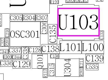
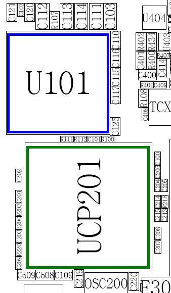
54 Main Electrical Parts List SEC CODE Design LOC Discription STATUS R512 C-CER,CHIP SA R513 C-CER,CHIP SA R514 C-CER,CHIP SA R515 C-CER,CHIP SA R516 C-CER,CHIP SA R517 C-CER,CHIP SA R518 C-CER,CHIP SA R519 C-CER,CHIP SA R520 C-CER,CHIP SA R521 C-CER,CHIP SA R522 C-CER,CHIP SA R523 C-CER,CHIP SA R524 C-CER,CHIP SA R525 C-CER,CHIP SA R527 C-CER,CHIP SA R529 C-CER,CHIP SA R530 C-CER,CHIP SA R531 C-CER,CHIP SA R532 C-CER,CHIP SA R533 C-CER,CHIP SA R536 C-CER,CHIP SA R537 C-CER,CHIP SA R538 C-CER,CHIP SA R539 C-CER,CHIP SA R540 C-CER,CHIP SA R541 C-TA,CHIP SA R542 C-TA,CHIP SA R543 C-TA,CHIP SA R544 C-TA,CHIP SA R546 C-TA,CHIP SA R547 C-TA,CHIP SA RFS400 C-TA,CHIP SA SIM100 C-TA,CHIP SA SW301 C-TA,CHIP SA SW302 C-TA,CHIP SA TCX400 C-TA,CHIP SA U100 C-TA,CHIP SA U102 C-TA,CHIP SA U103 C-TA,CHIP SA U107 C-TA,CHIP SA U108 C-TA,CHIP SA U202 INDUCTOR-SMD SA 10-9
55 Main Electrical Parts List SEC CODE Design LOC Discription STATUS U203 INDUCTOR-SMD SA U204 INDUCTOR-SMD SA U205 INDUCTOR-SMD SA U206 INDUCTOR-SMD SA U300 INDUCTOR-SMD SA U301 INDUCTOR-SMD SA U303 INDUCTOR-SMD SA U304 INDUCTOR-SMD SA U400 INDUCTOR-SMD SA U401 INDUCTOR-SMD SA U402 INDUCTOR-SMD SA U403 CRYSTAL-SMD SA U404 CRYSTAL-SMD SA U405 OSCILLATOR-VCTCXO SA U500 FILTER-EMI/ESD SA U501 FILTER-EMI/ESD SA U502 FILTER-EMI/ESD SA U504 FILTER-EMI/ESD SA UCD101 DUPLEXER-FEM SA UCD503 BEAD-SMD SA UCP201 BEAD-SMD SA UME200 BEAD-SMD SA V500 BEAD-SMD SA V501 BEAD-SMD SA V502 BEAD-SMD SA V503 BEAD-SMD SA V504 SWITCH-TACT SA V505 SWITCH-TACT SA ZD101 CONNECTOR-COAXIAL SA ZD201 CONNECTOR-FPC/FFC/PIC SA ZD202 CONNECTOR-CARD EDGE SA ZD203 CONNECTOR-CARD EDGE SA ZD204 SOCKET-INTERFACE SA ZD301 HEADER-BOARD TO BOARD SA ZD302 HEADER-BATTERY SA ZD303 ANTENNA-CHIP SA ZD304 BATTERY-LI(2ND) SA ZD305 BLUETOOTH MODULE SA GH A ZD500 IC MICOM SA GH A ZD501 IC ASIC SA GH A ZD502 NPR-ANTENNA CONTACT SA GH A ZD504 NPR-ANTENNA CONTACT SA 10-10
56 11. Flow Chart of Troubleshooting 11-1.Baseband Power ON 'Power On' does not work Check the current consumption Current consumption >= 100mA Download again Check the Vbat Voltage Voltage >=3.3V Charge the Battery Check the pin of U101 1 Pin#J12 >= 2.8V Check U101 and C115 2 Pin#A13 and pin#a14>=2.8v pin#c12 = 1.8V Check U101, U103 3 ChecktheclocksignalatC414 Freq = 26MHz Vrms >=300mV Vpp 900mV 4 Check the clock generation circuit (related to 3pin of TCX400, C407, R404) Check the initial operation END 11-1
57 DSP_DB(0:15) DSP_AB(0:8) DSP_IO DSP_RWN FLASH_RESET XOENA TX_BAND_SEL RX_SEL ANT_BAND_SEL SERLE SERDAT SERCLK TRXIP TRXIN TRXQP TRXQN DSP_DB(15) DSP_DB(14) DSP_DB(13) DSP_DB(12) DSP_DB(11) DSP_DB(10) DSP_DB(9) DSP_DB(8) DSP_DB(7) DSP_DB(6) DSP_DB(5) DSP_DB(4) DSP_DB(3) DSP_DB(2) DSP_DB(1) DSP_DB(0) DSP_AB(8) DSP_AB(7) DSP_AB(6) DSP_AB(5) DSP_AB(4) DSP_AB(3) DSP_AB(2) DSP_AB(1) DSP_AB(0) D2 D3 E3 E2 F3 F2 F1 F4 G4 G3 H5 J6 J5 K3 K1 K5 M1 N2 L5 K6 L2 E6 F5 A4 B3 A2 C2 DB15 DB14 DB13 DB12 DB11 DB10 DB9 DB8 DB7 DB6 DB5 DB4 DB3 DB2 DB0 AB8 AB6 AB4 AB2 AB0 RWN OCTL0 OCTL2 OCTL4 OCTL6 SERLE2 SERCK R108 TTY_DETECT VCCD_2_9 C102 U101 C125 VCCA_2_8 VCCD_1_8 VCCD_2_9 C101 C100 R100 VDD34 C11 VDD12 J13 UP_CLK N9 UP_RST R10 UP_IO P10 SIM_IO J11 SIM_RST K11 VSIM K12 VRTC H11 VIB_DRV F15 VLDO_7 C12 VLDO_6 A14 VL5S_B C9 VL5S_A D10 VLDO_5 B10 VL4S_B B11 VL4S_A A12 VLDO_4 B12 VLDO_3 A13 VLDO_2 J12 VLDO_1 G11 VACC F14 CSN_PSC R112 SDI_PSC K8 M7 VEXT E14 VBAT E13 CH_ISEN F12 CH_RES D14 VREF A10 CREF E9 VBAT VBAT C120 UP_SDO UP_SCLK UP_CS UP_SDI R107 R111 C103 KEYBL2 SIMCLK SIMDATA SIMRST INTRQ PWR_KEEP RST C105 C106 VBAT ICHRG C117 RTCALARM C107 C108 V1_8_EN GSM_TX_EN DCS_TX_EN C118 VCCA_2_8 C110 C111 VSYN_2_9 R106 R105 U102 C104 C112 VPAC_2_9 VRF_2_9 C113 VCCD_2_9 C114 VCLOCK C G G C115 C116 8 G SIM100 7 G 5 VRTC_1_5 C109 R101 M100 Flow Chart of Troubleshooting POS 1 NEG NC6 2 NC5 1 GNDS17 K10 GNDS16 J10 GNDS15 J9 GNDS14 J8 GNDS13 J7 GNDS12 H9 GNDS11 H8 GNDS10 H7 GNDS9 H6 GNDS8 G10 GNDS7 G9 GNDS6 G8 GNDS5 G7 GNDS4 F10 GNDS3 F9 GNDS2 F8 GNDS1 F7 AUX_ADC3 D13 GND_OCTL B4 VDD_OCTL C4 GNDV P13 VDDV L11 GNDB F6 VDDB A6 GNDD M10 VDDD N11 VSS4 P6 VSS3 R2 VSS2 K4 VSS1 G5 VDD_IO2 J4 VDD_IO1 N5 VDD3 N6 VDD2 M3 VDD1 J3 GND_HCUR F11 GND_PSC2 K15 GND_PSC1 B15 GNDQ E8 VDD67 B13 VDD5 C10 SIM_CLK K14 K2 DB1 K7 AB7 M2 AB5 N1 AB3 P1 AB1 L3 I O LED2_DRV G12 LED1_DRV G13 RING_DRV F13 R3 RESETN_CSP SCLK_PSC L8 C5 OCTL1 E5 OCTL3 G6 OCTL5 A3 OCTL7 SDO_PSC N7 CH_BDRV E11 B1 SERLE1 AFC TXP RXTXIP RXTXIN RXTXQP RXTXQN VXVCM VREGP VREGN XOENAQ MC INTRQ VIB_RNG_EN C1 SERDA ADC_AUX2 D15 ADC_AUX1 E10 RTC_ALMN H10 RAREF2 RAREF1 AOUTAP AOUTAN AOUTBP AOUTBN MICINP MICINN MICOUTP MICOUTN AUXINP AUXINN AUXOUTP AUXOUTN DAICK DAIRN DAIDI DAIDO RTC_CLK ADC_AUX4 DINTR PWR_SW2 PWR_SW1N PSW1_BUF RESET_O MODE PWR_KEEP D9 E7 B5 B6 D7 D6 C7 C6 P11 N12 R12 P12 N14 M14 N15 P15 M15 L14 K13 L13 R13 M13 R14 R4 P4 L6 M6 N4 D1 R6 P5 P3 C14 C15 L7 K9 N10 M9 L10 L9 C121 AOUTAP AOUTAN AOUTBP AOUTBN MICINP MICINN MICOUTP MICOUTN AUXINP AUXINN AUXOUTP AUXOUTN CLK32K XOENAQ CLK13M_MC AFC VAPC DSP_INT JIG_ON PWR_ON PSW1_BUF 11-2
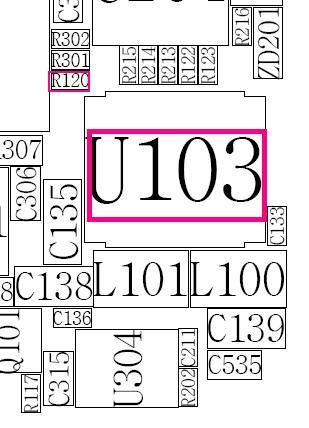
58 2 GND OUT 3 VCON 1 VCC 4 Flow Chart of Troubleshooting VRF_2_9 R401 13MHZ_BB R400 C400 CLK13M_TR R402 C401 CLK13M_MC TCX400 R434 CLK13M_WM AFC C407 R404 CLK26M_RF C408 C409 VCCD_1_6 VCCD_1_8 VBAT V1_8_EN U103 L101 1 VIN2 2 SW2 FB2 16 EN2 15 R120 C136 C138 3 PGND2 4 VDD EN1 14 NPOR2 13 R122 5 SGND NPOR1 12 R123 L100 6 PGND1 7 SW1 SCL 11 SDA 10 8 VIN1 FB1 9 C133 C139 C
59 Flow Chart of Troubleshooting VCLOCK L401 C412 U403 26M_REF_CLK C414 1 NC 2 A 3 GND 6 VCC NC 5 Y4 C415 R407 C416 8 VCC 1 _PR U404 CK 7 2 _CLR D Q _Q GND 4 13MHZ_BB 11-4

60 Flow Chart of Troubleshooting
61 Flow Chart of Troubleshooting Initial Initial Failure The pin #C12 of U101 = 1.8V and the pin #J12 of U101 = 1 Check the U101 (if it has some problem, it is to be replaced.) 2.8V? 1 Is the pin #K9 of U101 "Low High"? Check the U101 (if it has some problem, it is to be replaced.) There is kHz wave forms at the C216 and 2 Check the UCP201 C217 3 Is the pin #14 & #15 of U103 "High"? Check the U103, R120 The voltage is "High" at the C110,C115,C116 4 Check the U101 LCD display is O.K? Check the LCD part Sound is O.K? Check the Audio part END 11-6
62 P4 T2 5 B19 19 C18 17 E16 F16 E17 3 R4 U2 3 P3 2 N4 2 M3 1 M R17 K7 6 7 J6 5 J4 8 H6 4 H1 3 G6 4 H2 15 J13 13 L12 13 L15 14 M14 14 H19 F19 H P19 5 V17 V19 U16 U19 17 R13 SIMCLK SIMIO PIO07_USB_SUSP PIO11_USB_VMI PIO13_USB_VMO PIO36_USB_OEN PIO37_USB_DATA SPRXD0 SPTXD0_I2SD RIO_PIO01 DTR0_PIO03 TX0 CTS0_PIO29 PIO42_IRDARX TX1 KEYBRD1 KEYBRD3 KEYBRD5 KEYBRD7 KEYBRD9 KEYBRD11_PSW1_BUF PIO08_MCI_CMD PIO22_MCI_DAT1 PIO24_MCI_DAT3 PIO40_MCI_DAT_EN X1RTC X2RTC RTCALARMN PIO20_SYSCLKREQ PIO10 PIO25 PIO26 PIO27 PIO32 NC2 NC1 2 1 V SSA_U F1 8 VDDA_U F17 V SSA_D R1 1 V DDA_D T1 1 VSS18 M12 V SS17 M1 1 VSS16 M10 V SS15 M 9 VSS14 M8 V SS13 L 8 V SS12 L 7 V SS11 K 8 VSS10 J12 V SS9 H1 2 VSS8 H11 V SS7 H1 0 V SS6 H 9 V SS5 H 8 VSS4 G9 V SS3 G 8 VSS2 A18 V SS1 A 2 VDD_CORE8 V13 V DD_CORE7 V 7 N18 V DD_CORE5 M 2 VDD_CORE4 H18 V DD_CORE3 G 2 VDD_CORE2 B13 V B 8 VDD_IO_1P8_18 W18 VDD_IO_1P8_17 W8 VDD_IO_1P8_16 U12 V DD_IO_1P8_15 U 5 VDD_IO_1P8_14 U1 V DD_IO_1P8_13 T1 8 VDD_IO_1P8_12 P1 V DD_IO_1P8_11 L1 6 V DD_IO_1P8_10 L 4 V DD_IO_1P8_9 F 1 VDD_IO_1P8_8 D18 V DD_IO_1P8_7 D 9 VDD_IO_1P8_6 C14 V DD_IO_1P8_5 C 1 VDD_IO_1P8_4 B16 V DD_IO_1P8_3 B1 2 VDD_IO_1P8_2 B6 V DD_IO_1P8_1 B 4 VRTC G18 CKI W12 R ESTN G1 5 T MS W1 4 TRSTN R12 Flow Chart of Troubleshooting VCCD_1_6 VCCD_1_8 VRTC_1_5 C200 A(0:25) R203 CLK13M_TR TR_RST D(0:15) CP_WEN CP_OEN CHG_DET FLASH_RESET ROM1_CS ROM2_CS RAM1_CS RAM2_CS MV_CS LOWER_BYTE UPPER_BYTE D(0) D(1) D(2) D(3) D(4) D(5) D(6) D(7) D(8) D(9) D(10) D(11) D(12) D(13) D(14) D(15) A(0) A(1) A(2) A(3) A(4) A(5) A(6) A(7) A(8) A(9) A(10) A(11) A(12) A(13) A(14) A(15) A(16) A(17) A(18) A(19) A(20) A(21) A(22) A(23) A(24) A(25) SIMCLK SIMDATA SIMRST B7 C8 D8 A6 C6 C5 D7 E7 C4 C2 A3 B3 B1 D6 D5 D3 E8 F8 E6 D2 E4 E3 F5 F4 F3 F2 A8 E9 F9 G10 G11 F11 E11 G12 D11 E12 C12 A12 F12 D12 E13 D13 D14 B14 E14 H14 A14 C15 G14 J14 D15 C16 F15 B17 H16 A17 A_A0 A_A1 A_A2 A_A3 A_A4 A_A5 A_A6 A_A7 A_A8 A_A9 A_A10 A_A11 A_A12 A_A13 A_A14 A_A15 A_A16 A_A17 A_A18 A_A19 A_A20 A_A21 A_A22 A_A23 A_A24 PIO35_A_A25_BOOTSEL A_D0 A_D1 A_D2 A_D3 A_D4 A_D5 A_D6 A_D7 A_D8 A_D9 A_D10 A_D11 A_D12 A_D13 A_D14 A_D15 A_WEN A_OEN PIO30_WAITN FLASHRSTN A_CS0N A_CS1N A_CS2N A_CS3N A_CS4N A_CS5N A_CS6N A_CS7N A_BE0N A_BE1N P PIO14_SIMRS T C PIO09_USB_VP I D PIO12_USB_VP O R SPCLK 0 T SPFS 0 P DSR0_PIO0 2 N RTS0_PIO0 4 M RX0_IRQ2 8 N DCD0_PIO4 4 R PIO41_IRDAT X L RX1_IRQ2 8 J KEYBRD 0 VDD_CORE6 J KEYBRD 2 J KEYBRD 4 H KEYBRD 6 DD_CORE1 UCP201 H KEYBRD 8 G KEYBRD1 0 J PIO38_MCI_CL K K PIO21_MCI_DAT 0 L PIO23_MCI_DAT 2 L PIO39_MCI_CMD_E N N PIO43_MCI_DAT0_E N G OSC32OU T P PIO19_PWRKEE P G PWM1_PIO4 6 TDO TDI TCK CKO_IACK IOBIT1_PIO06 IOBIT0_PIO05 SPFS1_PIO15 SPTXD1_I2SD_PIO16 SPRXD1_PIO17 SPCLK1_PIO18 INT0 IO RWN D_D15 D_D14 D_D13 D_D12 D_D11 W PIO2 8 D_D10 D_D9 D_D8 D_D7 D_D6 D_D5 D_D4 D_D3 D_D2 D_D1 D_D0 D_A8 D_A7 D_A6 D_A5 D_A4 D_A3 D_A2 D_A1 D_A0 TEST3 TEST2 TEST1 CPTSTSTOP_CKO ATDO_PWM2 ATDI_RTS1 ATCK_CTS1 ATMS_PIO45 PIO31_IRQ6 PIO00_IRQ5 IRQ4 IRQ3 IRQ2 IRQ1 PIO47 PIO34 PIO33 T12 V14 U14 N12 N11 V12 N15 N16 M17 M18 T15 W6 V6 P11 N10 N9 N8 P9 P8 R9 T9 T8 U8 V8 R8 T7 R7 T6 U6 R6 N6 V4 T5 U4 V3 W3 W2 V1 V16 T14 U15 T17 T13 L5 M4 K12 P12 P16 P18 P17 M19 M16 J16 R14 U18 R220 DSP_TMS DSP_TDO DSP_TDI DSP_TCK PCM_SYNC PCM_TXD PCM_RXD PCM_CLK DSP_INT DSP_IO DSP_RWN CP_TDO CP_TDI CP_TCK CP_TMS WM_SDIN WM_CS MV_INT FLIP_SNS JACK_INT INTRQ WM_SCLK USB_CON CF DSP_DB(15) DSP_DB(14) DSP_DB(13) DSP_DB(12) DSP_DB(11) DSP_DB(10) DSP_DB(9) DSP_DB(8) DSP_DB(7) DSP_DB(6) DSP_DB(5) DSP_DB(4) DSP_DB(3) DSP_DB(2) DSP_DB(1) DSP_DB(0) DSP_AB(8) DSP_AB(7) DSP_AB(6) DSP_AB(5) DSP_AB(4) DSP_AB(3) DSP_AB(2) DSP_AB(1) DSP_AB(0) DSP_DB(0:15) DSP_AB(0:8) USB_SUSP USB_DET CAM_IC_RESET USB_VPO USB_VMO USB_OEN USB_DATA UP_SCLK UP_SDO UP_SDI UP_CS CHG_EN BT_EN T_FLASH_ON AS4 EAR_SWITCH AS2 CODEC_PDN CARD_DETECT AMP_EN BL_CONT XOENAQ PWR_KEEP CLK32K RTCALARM DEBUG_RTS DEBUG_TXD DEBUG_RXD DEBUG_CTS OSC MAIN_EL_EN MOT_EN EL_IC_EN C219 C220 SDS_TXD SDS_RXD KEY_COL(0:4) PSW1_BUF KEY_ROW(0:5) KEY_COL(0) KEY_COL(1) KEY_COL(2) KEY_COL(3) KEY_COL(4) KEY_ROW(0) KEY_ROW(1) KEY_ROW(2) KEY_ROW(3) KEY_ROW(4) KEY_ROW(5) MCI_DAT0_EN MCI_DAT_EN MCI_CMD_EN MCI_DAT0 MCI_CMD MCI_CLK 11-7

63 Flow Chart of Troubleshooting
64 Flow Chart of Troubleshooting Sim Part "Insert SIM is displayed on the LCD Check the SIM connector's (SIM100) connection to SIM card 1 Resolder or change SIM100 2 Check the voltage at pin#1 of SIM100 >= 2.8V? Check the U101 Is there any signals pin#2,#3,#4 of? 3 Check the UCP201 Check the SIM Card END
65 Flow Chart of Troubleshooting Microphone Part Microphone does not work Is the assembled status of microphone O.K? Reassembled the microphone Check the reference voltage on mic path C V? Is microphone ok? 1 Resolder or change R500,R501,R502,R505,R514,R517, C502,C505 2 Check U101 END 11-10
66 Flow Chart of Troubleshooting MICOUTP R500 R501 C502 MICINP MICINN MICOUTN R505 R502 C505 C503 R504 C508 C509 MAIN_MIC_P MAIN_MIC_N VCCA_2_8 R514 AUXOUTP AUXINP R516 R518 C514 R519 R517 AUXINN AUXOUTN R524 R523 C519 C516 EAR_MIC_P EAR_MIC_N R521 C515 R520 C
67 Flow Chart of Troubleshooting Speaker Part_1(MP3, SPEAKER PHONE) There is no sound from the Speaker Is the terminal of Speaker O.K? Replace the Speaker Are there any signals at the L500, L501 1 Check U501 MP3 Whatisthetypeof sound from the Speaker SPEAKER PHONE Is there any signals at the pin#12 and pin#13 of UCD503? Is there any signals at C506, C512? 2 Check UCD503 The pin #5, #7 of U500 is "High" The pin #5, #7 of U500 is "High" 3 Check U101 4 Check UCP201 END 11-12
68 VSS VSS VDD VDD GND VDD VDD VDD VDD Flow Chart of Troubleshooting VBAT C500 L NC C504 AMP_OUT_N 19 NC VOM 12 AMP_IN_P AMP_IN_N C506 C512 R503 R512 1 VREF 2 VIM 3 VIP U501 VSS 11 VSS 10 VOP 9 L501 C510 4 EN AMP_OUT_P AMP_EN R515 R546 R547 R513 C513 VBAT C517 VBAT L504 C501 AOUTAP R511 U500 1 NO2 10 VCC 2 NO1 COM2 9 R508 AOUTAN SPK_N SPK_P 3 COM1 NC2 8 AMP_OUT_P AMP_OUT_N 4 NC1 IN2 7 C551 5 IN1 GND 11 GND 6 C550 AS2 R
69 PLLGND MONOOUT OUT3 ROUT1 LOUT1 HPGND ROUT2 LOUT2 SCLK SDIN LINEINL LINEINR GND GND GND CSB MODE MONOIN+ MONOIN- Flow Chart of Troubleshooting VCCD_1_8 R525 R527 C520 C522 AOUTAN AOUTAP WM_CS WM_SDIN WM_SCLK CLK13M_WM R543 R544 C533 C GND 37 NC5 38 NC4 1 MCLK 2 DCVDD 3 DBVDD 4 DGND 5 BCLK UCD503 NC HPDETECT NC VMID 20 VREF AGND 19 C529 C532 C530 C531 VDAC_3_1 PCM_CLK PCM_TXD PCM_SYNC R532 R531 6 DACDAT 7 DACLRC 8 CLKOUT AVDD HPVDD 17 C536 C537 R533 AMP_IN_N AMP_IN_P MP3_L MP3_R 11-14

70 Flow Chart of Troubleshooting
71 Flow Chart of Troubleshooting Speaker Part_2(RECEIVER) There is no sound from the Speaker Is the terminal of Speaker O.K? Replace the Speaker Are there any signals at the PIN#3, #9 of U500 1 Check U500 The pin #5, #7 of U500 is "Low" 2 Check UCP201 Are there any signals at the PIN#2, #10 of U500 3 Check U101 4 Check UCP201 END 11-16

72 Flow Chart of Troubleshooting
73 Flow Chart of Troubleshooting Charging Part Abnormal charging part The pin #1 of U108 is VEXT 뵃 5V? Check IF501 1 The pin #6 of U108 is "LOW"? Check UCP201 2 Charging Current is 350mA~650mA? Check U108 3 Check The Battery END 11-18

74 Flow Chart of Troubleshooting
75 GND ZD ZD ZD502 ZD Flow Chart of Troubleshooting VBAT USB_5V VEXT_5V VCCD_1_8 R536 R537 IFC501 EAR_MIC_P EAR_MIC_N EAR_R EAR_GND EAR_L EAR_SWITCH JACK_INT TTY_DETECT SDS_TXD SDS_RXD JIG_ON_IF USB_DPLS USB_DMNS R538 R539 R V500 C541 V505 C547 C542 C NC 22 NC 23 NC 24 NC NC 25 NC 26 NC 27 NC 28 V501 V502 V503 V504 VEXT_5V VBAT ICHRG U108 1 IN BATT 8 2 VL ACOK 7 3 GND EN 6 4 ISET CHG 5 CHG_EN C137 C124 C123 R110 9 C122 R
76 Flow Chart of Troubleshooting RF GSM850/EGSM RX NORMAL CONDITION catch the channel? 1 CHECK ANT401, R405 contact? DUF400 Check Pin1-65dBm? 2 C421, RFS400 resolder or change DUF400 Check Pin10, 11-65dBm? 3 DUF400 resolder or change U405 Check Pin6, 7-65dBm? 4 C431, C436, L406 resolder or change U405 Check Pin1, 31, 48 : 2.9V? 5 U101 pin A13, B10, C112, C114 resolder or change U405 Check Pin35 : 26Mhz? Vp-p : 950mV? 6 TCX400 resolder or change U405 Check Pin25, 26, 27, 28 Vp-p : 120mV? 7 U405 resolder or change 8 U101 CHECK!! 11-21

77 Flow Chart of Troubleshooting
78 Flow Chart of Troubleshooting DCS RX NORMAL CONDITION catch the channel? 1 CHECK ANT401, R405contact? DUF400 Check Pin1-65dBm? 2 C421, RFS400 resolder or change DUF400 Check Pin12, 13-65dBm? 3 DUF400 resolder or change U405 Check Pin4, 5-65dBm? 4 C429, C430, L405 resolder or change U405 Pin1, 31, 48 : 2.9V? 5 U101 pin A13, B10, C113, C115 resolder or change U405 Check Pin35 : 26Mhz? Vp-p : 950mV? 6 TCX400 resolder or change U405 Check Pin25, 26, 27, 28 Vp-p : 120mV? 7 U405 resolder or change 8 U101 CHECK!! 11-23
79 Flow Chart of Troubleshooting
80 Flow Chart of Troubleshooting PCS RX NORMAL CONDITION catch the channel? 1 CHECK ANT401, R405contact? DUF400 Check Pin1-65dBm? 2 C421, RFS400 resolder or change DUF400 Check Pin14, 15-65dBm? 3 DUF400 resolder or change U405 Check Pin2, 3-65dBm? 4 C427, C428, L404 resolder or change U405 Pin1, 31, 48 : 2.9V? 5 U101 pin A13, B10, C113, C115 resolder or change U405 Check Pin35 : 26Mhz? Vp-p : 950mV? 6 TCX400 resolder or change U405 Check Pin25, 26, 27, 28 Vp-p : 120mV? 7 U405 resolder or change 8 U101 CHECK!! 11-25
81 Flow Chart of Troubleshooting GSM850/EGSM TX PAM406 pin 13 : about 32dBm? DUF400 pin 8 : 2.6V? 1 U101 check & change 2 C421,RFS400 R405,ANT401 check & change PAM406 pin13: about 32dBm? 3 DUF400 check & change PAM406 pin16, 17: 3.7V? BATTERY check & change PAM406 pin 6 : 2.9V? 4 U405 pin21 check PAM406 pin7 about 5dBm? PAM406 pin 2,3 : 3V? 5 PAM406 check & change 1 U101 check U405 pin16,41,31,29 : 2.9V? 7 U101 pin A13, B10, C112, C114 check or resolder U405 pin35 : 26MHz? Vp-p : 950mV? 6 TCX400 check or resolder U405 pin25,26,27,28 Vp-p=1V? 1 U101 check or resolder 8 U405 check or resolder 11-26

82 Flow Chart of Troubleshooting
83 Flow Chart of Troubleshooting DCS/PCS TX U404 pin 13 : about 30dBm? DUF400 pin 3 : 2.6V? 1 U101 check & change 2 C421,RFS400 R405,ANT401 check & change PAM406 pin19: about 30dBm? 3 DUF400 check & change PAM406 pin16, 17: 3.7V? BATTERY check & change PAM406 pin 6 : 2.9V? 4 U405 pin21 check PAM406 pin1 about 5dBm? 5 PAM406 pin 2 : 0V? pin 3 : 3V? PAM406 check & change 1 U101 check U405 pin16,41,31,29 : 2.9V? 7 U101 pin A13, B10, C112, C114 check or resolder U405 pin35 : 26MHz? Vp-p : 950mV? 6 TCX400 check or resolder U405 pin25,26,27,28 Vp-p=1V? 1 U101 check or resolder 8 U405 check or resolder 11-28
84 DEBUG_RTS DEBUG_CTS DEBUG_TXD DEBUG_RXD R413 CLK26M_RF 26M_REF_CLK SERDAT SERCLK R435 R436 C406 VSYN_2_9 C443 VBT_1_8 SERLE VSYN_2_9 R403 RESETB UART_CTS UART_RTS UART_RX U401 PCM_OUT UART_TX PCM_SYNC VDD_1.8V PIO_0 VDD_REG PIO_1 VDD_UART PIO_2 PIO_3 GND PIO_4_UART_TX2 GND PIO_5_UART_RTS2 GND PIO_6_UART_CTS2 GND PIO_7_UART_RX2 GND TRXIP TRXIN TRXQP TRXQN ANT PCM_CLK PCM_IN C426 C448 C449 TXON_B5 DCS_PAM_IN GSM_PAM_IN R437 0 C418 C417 VRF_2_9 R418 PCM_CLK PCM_TXD PCM_RXD PCM_SYNC R428 R432 R410 R408 R417 R409 R427 R R429 AN VCCVCXO VCXOB VCXOOUT1 SDATA CLK VCCBB CPIFSYN VCCIFSYN IOUT/IIN VSYN_2_9 IOUTB/IINB QOUT/QIN QOUTB/QINB 24 R VPAC_2_9 C453 C457 C C419 C U C VRF_2_9 C450 XOENA BT_EN C C458 VRF_2_ NC NC 54 VCCLNA 1 PCSLNAI 2 PCSLNAIB 3 DCSLNAI GSMLNAI 4 DCSLNAIB 5 6 GSMLNAIB 7 14 VCCTX1 8 DMIXIN 9 13 C404 R406 C422 C452 VBAT VCLOCK R423 R430 C410 VRF_2_9 C451 3 VBAT VIN C425 U400 2 R411 GND 6 GND 6 NC 5 U402 NC 5 3 VIN VOUT 4 VAPC R412 VRF_2_9 DCS_PAM_IN GSM_PAM_IN TXON_B5 R421 C405 C411 C442 C455 VBT_1_8 26M_REF_CLK C427 C428 C429 C430 C431 C436 VPAC_2_9 C454 AFC C415 PA_COU_OUT 7 PIN_GSM 3 VREG 6 TX_ON 17 VBAT L404 L405 L406 C414 C408 VCLOCK L401 C446 PAM A POUT_XCS 19 COUPLEROUT_GSM 12 COUPLEROUT_XCS 20 BAND 2 TCX400 U403 R407 VCC 8 U404 VCC CK 7 _CLR D 6 5 Q _Q GND 4 C447 VBAT Y 4 C456 6 VRF_2_9 R401 C412 C416 C409 L412 TX_BAND_SEL 13MHZ_BB C407 13MHZ_BB L411 R404 L410 R400 R402 R434 R426 L407 R424 C439 C400 C401 7 R425 DUF400 GSM850/EGSM-TX 10 GSM850/EGSM-RX1 11 GSM850/EGSM-RX2 14 PCS_RX1 15 PCS_RX2 5 DCS/PCSTX C438 1 ANT DCS_RX1 DCS_RX2 G G G G G G G G G G R419 R422 VC3 CLK13M_TR CLK13M_MC CLK13M_WM CLK26M_RF C421 47PF 47PF 47PF R420 L403 L402 R405 PA_COU_OUT ANT C413 DCS_TX_EN GSM_TX_EN RX_SEL ANT401 ANT402 1 RFS400 A C Flow Chart of Troubleshooting G 4 G VC1 3 8 VC2 4 3 VCC OUT NC 5 VCON 1 2 GND 1 NC 3 GND 1 _PR 1 PIN_XCS POUT_GSM 13 5 VRAMP 16 VBAT VLDO 15 NC N N NC 8 G 10 G 11 G G G 2 G 24 G 25 G 4 C C C445 2 GND VOUT 4 1 STBY 1 STBY GND G 52 DMIXINB 10 BIASDAC 11 LDO_CONT PF C444 G G G CAPI VCCMIX AMDETO AM_CONT CAPIB RAMPDAC CAPQ VCCTXVCO CAPQB TXOUTG VCCRFLO TXOUTD VCCRFVCO TXVCOGB L409 VCCRFSYN TXVCOG L408 CPRFSYN TXON FLOCK VCCTX2 PMBW LE PMDETO VCXOOUT2 C435 C440 C
85 12. PCB Diagrams 12-1 AN400 ANT401 ANT402 ANT_J BTC502 CD200 D504 DUF400 G1 G2 G3 IFC501 M100 Q100 RFS400 RST SIM100 SW302 SW301 TCK TDI TDOTMS TP201 TP301 TP302 TP303 TP_GND U102 U107 U202 U400 U401 U402 U500 U501 U502 U504 UCD503 V501 V502 V503 V504 WEN ZD302 ZD305 ZD502 ZD504
86 PCB Diagrams 12-2 CN300 F301 F302 F303 F304 GND_J HDC301 JIG_ON_J OSC200 OSC301 PAM406 Q101 SDS_RXD_J SDS_TXD_J SOC302 TCX400 U100 U101 U103 U108 U203 U204 U205 U U 1 U30 U303 U304 U403 U404 U405 UCP201 UME200 USB_5V_J USB_DMNS_J USB_DPLS_J V500 V505 VBAT_J ZD201 ZD202 ZD203 ZD204 ZD301 ZD303 ZD304 ZD306 ZD500 ZD501

87 13. Block Diagrams RF Solution Block Diagram 13-1
GSM TELEPHONE SGH-D900 GSM TELEPHONE CONTENTS. 1. Safety Precautions. 2. Specification. 3. Product Function. 4. Array course control
 GSM TELEPHONE SGH-D900 GSM TELEPHONE CONTENTS 1. Safety Precautions 2. Specification 3. Product Function 4. Array course control 5. Exploded View and Parts List 6. MAIN Electrical Parts List 7. Block Diagrams
SERVICE Manual GSM TELEPHONE SGH-E Specification. 2. Flow Chart of Troubleshooting. 3. Exploded Views and Parts List. 4. Electrical Parts List
 GSM TELEPHONE SGH-E310 SERVICE Manual GSM TELEPHONE CONTENTS 1. Specification 2. Flow Chart of Troubleshooting 3. Exploded Views and Parts List 4. Electrical Parts List 5. Block Diagrams 6. PCB Diagrams
UMTS TELEPHONE SGH-L760 UMTS TELEPHONE CONTENTS. 1. Safety Precautions. 2. Specification. 3. Product Function. 4. Array course control
 UMTS TELEPHONE SGH-L760 UMTS TELEPHONE CONTENTS 1. Safety Precautions 2. Specification 3. Product Function 4. Array course control 5. Exploded View and Parts List 6. MAIN Electrical Parts List 7. Block
GSM TELEPHONE SGH-X500 GSM TELEPHONE CONTENTS. 1. Safety Precautions. 2. Specification. 3. Product Function. 4. Array course control
 GSM TELEPHONE SGH-X500 GSM TELEPHONE CONTENTS 1. Safety Precautions. Specification 3. Product Function 4. Array course control 5. Exploded View and Parts List 6. Disassembly and Assembly instructions 7.
SERVICE Manual GSM TELEPHONE SGH-E Specification. 2. Flow Chart of Troubleshooting. 3. Exploded Views and Parts List. 4. Electrical Parts List
 GSM TELEPHONE SGH-E300 SERVICE Manual GSM TELEPHONE CONTENTS 1. Specification 2. Flow Chart of Troubleshooting 3. Exploded Views and Parts List 4. Electrical Parts List 5. Block Diagrams 6. PCB Diagrams
GSM TELEPHONE. SGH-i710 GSM TELEPHONE CONTENTS. 1. Safety Precautions. 2. Specification. 3. Operation Instruction and Installation
 GSM TELEPHONE SGH-i710 GSM TELEPHONE CONTENTS 1. Safety Precautions 2. Specification 3. Operation Instruction and Installation 4. Array course control 5. Exploded View/Disassembly and Assembly Instructions
SGH-M Specification. 2. Exploded View and Parts list. 3. Chart of Troubleshooting. 4. Array course control. 5. Block Diagrams. 6.
 GSM TELEPHONE SGH-M300 GSM TELEPHONE CONTENTS 1. Specification 2. Exploded View and Parts list 3. Chart of Troubleshooting 4. Array course control 5. Block Diagrams 6. PCB Diagrams 7. MAIN Electrical Parts
GSM TELEPHONE SGH-T619 GSM TELEPHONE CONTENTS. 1. Safety Precautions. 2. Specification. 3. Product Function. 4. Array course control
 GSM TELEPHONE SGH-T619 GSM TELEPHONE CONTENTS 1. Safety Precautions 2. Specification 3. Product Function 4. Array course control 5. Exploded View/Disassembly and Assembly Instructions 6. MAIN Electrical
GSM TELEPHONE SGH-J700 GSM TELEPHONE CONTENTS. 1. Safety Precautions. 2. Specification. 3. Product Function. 4. Array course control
 GSM TELEPHONE SGH-J700 GSM TELEPHONE CONTENTS 1. Safety Precautions 2. Specification 3. Product Function 4. Array course control 5. Exploded View and Parts List 6. Main Electrical Parts List 7. Block Diagrams
SGH-M Specification. 2. Exploded View and Parts list. 3. Chart of Troubleshooting. 4. Array course control. 5. Block Diagrams. 6.
 GSM TELEPHONE SGH-M300 GSM TELEPHONE CONTENTS 1. Specification 2. Exploded View and Parts list 3. Chart of Troubleshooting 4. Array course control 5. Block Diagrams 6. PCB Diagrams 7. MAIN Electrical Parts
GSM TELEPHONE SGH-X550 GSM TELEPHONE CONTENTS. 1. Safety Precautions. 2. Specification. 3. Operation Instruction and Installation
 GSM TELEPHONE SGH-X550 GSM TELEPHONE CONTENTS 1. Safety Precautions 2. Specification 3. Operation Instruction and Installation 4. Array course control 5. Exploded View/Disassembly and Assembly Instructions
GSM TELEPHONE SGH-E380 GSM TELEPHONE CONTENTS. 1. Safety Precautions. 2. Specification. 3. Product Function. 4. Array course control
 GSM TELEPHONE SGH-E380 GSM TELEPHONE CONTENTS 1. Safety Precautions 2. Specification 3. Product Function 4. Array course control 5. Exploded View and Parts List 6. MAIN Electrical Parts List 7. Block Diagrams
GSM TELEPHONE SGH-G600 GSM TELEPHONE CONTENTS. 1. Safety Precautions. 2. Specification. 3. Product Function. 4. Array course control
 GSM TELEPHONE SGH-G600 GSM TELEPHONE CONTENTS 1. Safety Precautions 2. Specification 3. Product Function 4. Array course control 5. Exploded View and Part List 6. MAIN Electrical Parts List 7. Block Diagrams
GSM TELEPHONE. SGH-D900i CONTENTS. 1. Safety Precautions. 2. Specification. 3. Operation Instruction and Installation. 4. Array course control
 GSM TELEPHONE SGH-D900i GSM TELEPHONE CONTENTS 1. Safety Precautions 2. Specification 3. Operation Instruction and Installation 4. Array course control 5. Exploded View/Disassembly and Assembly Instructions
GSM TELEPHONE SGH-P310 GSM TELEPHONE CONTENTS. 1. Safety Precautions. 2. Specification. 3. Product Function. 4. Array course control
 GSM TELEPHONE SGH-P310 GSM TELEPHONE CONTENTS 1. Safety Precautions 2. Specification 3. Product Function 4. Array course control 5. Exploded View and Parts List 6. MAIN Electrical Parts List 7. Block Diagrams
GSM TELEPHONE SGH-D830 GSM TELEPHONE CONTENTS. 1. Safety Precautions. 2. Specification. 3. Product Function. 4. Array course control
 GSM TELEPHONE SGH-D830 GSM TELEPHONE CONTENTS 1. Safety Precautions 2. Specification 3. Product Function 4. Array course control 5. Exploded View and Parts List 6. MAIN Electrical Parts List 7. Block Diagrams
SERVICE Manual GSM TELEPHONE SGH-E Specification. 2. Exploded Views and Parts List. 3. Electrical Parts List. 4. Flow Chart of Troubleshooting
 GSM TELEPHONE SGH-E400 SERVICE Manual GSM TELEPHONE CONTENTS 1. Specification 2. Exploded Views and Parts List 3. Electrical Parts List 4. Flow Chart of Troubleshooting 5. Block Diagrams 6. PCB Diagrams
1. GSM General Specification
 SERVICE Manual ELECTRONICS 1. GSM General Specification GSM900 Phase 1 EGSM 900 Phase 2 DCS1800 Phase 1 PCS1900 Freq. Band[MHz] Uplink/Downlink 890~915 935~960 880~915 925~960 1710~1785 1805~1880 1850~1910
GALILEO Timing Receiver
 GALILEO Timing Receiver The Space Technology GALILEO Timing Receiver is a triple carrier single channel high tracking performances Navigation receiver, specialized for Time and Frequency transfer application.
Memec Spartan-II LC User s Guide
 Memec LC User s Guide July 21, 2003 Version 1.0 1 Table of Contents Overview... 4 LC Development Board... 4 LC Development Board Block Diagram... 6 Device... 6 Clock Generation... 7 User Interfaces...
V6118 EM MICROELECTRONIC - MARIN SA. 2, 4 and 8 Mutiplex LCD Driver
 EM MICROELECTRONIC - MARIN SA 2, 4 and 8 Mutiplex LCD Driver Description The is a universal low multiplex LCD driver. The version 2 drives two ways multiplex (two blackplanes) LCD, the version 4, four
RF4432F27 wireless transceiver module
 RF4432F27 wireless transceiver module 1. Description RF4432F27 is 500mW RF module embedded with amplifier and LNA circuit. High quality of component, tightened inspection and long term test make this module
SA9504 Dual-band, PCS(CDMA)/AMPS LNA and downconverter mixers
/AMPS LNA and downconverter mixers") INTEGRATED CIRCUITS Supersedes data of 1999 Aug 4 1999 Oct 8 DESCRIPTION The is an integrated receiver front-end for 900 MHz Cellular (AMPS) and 1.9 GHz PCS (CDMA) phones. This dual-band receiver circuit
INTEGRATED CIRCUITS Supersedes data of 1999 Aug 4 1999 Oct 8 DESCRIPTION The is an integrated receiver front-end for 900 MHz Cellular (AMPS) and 1.9 GHz PCS (CDMA) phones. This dual-band receiver circuit
RF4432 wireless transceiver module
 RF4432 wireless transceiver module 1. Description RF4432 adopts Silicon Lab Si4432 RF chip, which is a highly integrated wireless ISM band transceiver. The features of high sensitivity (-121 dbm), +20
A MISSILE INSTRUMENTATION ENCODER
 A MISSILE INSTRUMENTATION ENCODER Item Type text; Proceedings Authors CONN, RAYMOND; BREEDLOVE, PHILLIP Publisher International Foundation for Telemetering Journal International Telemetering Conference
N720 Specifications Version 1.4
 N720 Hardware User Guide () N720 Specifications Version 1.4 Copyright Copyright 2017 Neoway Technology Co., Ltd. All rights reserved. No part of this document may be reproduced or transmitted in any form
EEM Digital Systems II
 ANADOLU UNIVERSITY DEPARTMENT OF ELECTRICAL AND ELECTRONICS ENGINEERING EEM 334 - Digital Systems II LAB 3 FPGA HARDWARE IMPLEMENTATION Purpose In the first experiment, four bit adder design was prepared
SignalTap Plus System Analyzer
 SignalTap Plus System Analyzer June 2000, ver. 1 Data Sheet Features Simultaneous internal programmable logic device (PLD) and external (board-level) logic analysis 32-channel external logic analyzer 166
TABLE OF CONTENTS. Instructions:
 TABLE OF CONTENTS Instructions: 1 Overview 1 2 Main technical parameters 1 3 Display and keyboard 2 3.1 Display Window 2 3.2 Indicator 4 4. Operation 4 4.1 Power 4 4.2 Zero 4 Modified 4 4.3 Modified 4
Assembly Level Service Guide
 Assembly Level Service Guide This guide describes how to service the Agilent 53150A, 53151A, and 53152A Microwave Frequency Counters. The information in this guide applies to instruments having the number
Semiconductor Devices. Microwave Application Products. Microwave Tubes and Radar Components
 Microwave Application Products Microwave Tubes and Radar Components Our semiconductor products are mostly analog semiconductors classified broadly into three groups: Bipolar ICs, MOS ICs, and Microwave
USER'S MANUAL. Getting started with ALEXAN ATMEL AT89C2051/AT89C4051 Training Module - 1
 USER'S MANUAL Getting started with ALEXAN ATMEL AT89C05/AT89C405 Training Module - Version.0 Copyright 006 Ace Electronic Technology Inc. All Rights Reserved Alexan 05/405 TM- v..0 Page of 7 About This
GSM TELEPHONE SGH-D Specification. 2. Circuit Description. 3. Exploded Views and Parts List. 4. Electrical Parts List. 5.
 GSM TELEPHONE SGH-D820 1. Specification 2. Circuit Description 3. Exploded Views and Parts List 4. Electrical Parts List 5. Block Diagrams 6. PCB Diagrams 7. Flow Chart of Troubleshooting This Service
ANALOG I/O MODULES AD268 / DA264 / TC218 USER S MANUAL
 UM-TS02 -E026 PROGRAMMABLE CONTROLLER PROSEC T2-series ANALOG I/O MODULES AD268 / DA264 / TC218 USER S MANUAL TOSHIBA CORPORATION Important Information Misuse of this equipment can result in property damage
MSP430-HG2231 development board Users Manual
 MSP0-HG development board Users Manual All boards produced by Olimex are ROHS compliant Revision Initial, June 0 Copyright(c) 0, OLIMEX Ltd, All rights reserved Page INTRODUCTION: MSP0-HG is header board
RF V W-CDMA BAND 2 LINEAR PA MODULE
 3 V W-CDMA BAND 2 LINEAR PA MODULE Package Style: Module, 10-Pin, 3 mm x 3 mm x 1.0 mm Features HSDPA and HSPA+ Compliant Low Voltage Positive Bias Supply (3.0 V to 4.35 V) +28.5 dbm Linear Output Power
apple Service Source Apple Cinema HD Display 23" LCD (ADC) 11 April Apple Computer, Inc. All rights reserved.
 11 April Apple Computer, Inc. All rights reserved.") apple Service Source Apple Cinema HD Display 23" LCD (ADC) 11 April 2003 2003 Apple Computer, Inc. All rights reserved. apple Service Source Take Apart Apple Cinema HD Display 23" LCD (ADC) 2003 Apple
apple Service Source Apple Cinema HD Display 23" LCD (ADC) 11 April 2003 2003 Apple Computer, Inc. All rights reserved. apple Service Source Take Apart Apple Cinema HD Display 23" LCD (ADC) 2003 Apple
MONITOR POWER Shiloh Road Alpharetta, Georgia (770) FAX (770) Toll Free
 FAX (770) Toll Free") Instruction Manual Model 2099-10xx 10MHz Frequency Source April 2014, Rev. H MENU INTERNAL LEVEL = +10dBm MONITOR POWER 1 2 MODEL 2099 FREQUENCY SOURCE CROSS TECHNOLOGIES INC. ALARM OVEN REMOTE EXECUTE
Instruction Manual Model 2099-10xx 10MHz Frequency Source April 2014, Rev. H MENU INTERNAL LEVEL = +10dBm MONITOR POWER 1 2 MODEL 2099 FREQUENCY SOURCE CROSS TECHNOLOGIES INC. ALARM OVEN REMOTE EXECUTE
SingMai Electronics SM06. Advanced Composite Video Interface: HD-SDI to acvi converter module. User Manual. Revision 0.
 SM06 Advanced Composite Video Interface: HD-SDI to acvi converter module User Manual Revision 0.4 1 st May 2017 Page 1 of 26 Revision History Date Revisions Version 17-07-2016 First Draft. 0.1 28-08-2016
PLL1920M LED LCD Monitor
 PLL1920M LED LCD Monitor USER'S GUIDE www.planar.com Content Operation Instructions...1 Safety Precautions...2 First Setup...3 Front View of the Product...4 Rear View of the Product...5 Installation...6
TV-1800C (PAL B / G,H) TV-1800D (PAL I) TV-1800I (PAL B / G) TV-1800N (PAL B / G,H)
 TV-1800D (PAL I) TV-1800I (PAL B / G) TV-1800N (PAL B / G,H)") < TUNING > (without price) TV-1800C (PAL B / G,H) TV-1800D (PAL I) TV-1800I (PAL B / G) TV-1800N (PAL B / G,H) (KX-523) DEC. 1996 R CONTENTS Page SPECIFICATIONS... 1 BLOCK DIAGRAM... 2 CIRCUIT OPERATIONS...
< TUNING > (without price) TV-1800C (PAL B / G,H) TV-1800D (PAL I) TV-1800I (PAL B / G) TV-1800N (PAL B / G,H) (KX-523) DEC. 1996 R CONTENTS Page SPECIFICATIONS... 1 BLOCK DIAGRAM... 2 CIRCUIT OPERATIONS...
INSTALLATION MANUAL FT-FOTR-1VDE-ST-S
 INSTALLATION MANUAL FT-FOTR-1VDE-ST-S 1-Channel Digital Duplex Baseband Video Transmitter and Receiver With Reverse Data Transmission & Ethernet Transmission v1.0 4/5/11 1 PACKAGE CONTENTS This package
Overview of BDM nc. The IEEE JTAG specification is also recommended reading for those unfamiliar with JTAG. 1.2 Overview of BDM Before the intr
 Application Note AN2387/D Rev. 0, 11/2002 MPC8xx Using BDM and JTAG Robert McEwan NCSD Applications East Kilbride, Scotland As the technical complexity of microprocessors has increased, so too has the
IC-F300/F400/S SERIES PRECAUTIONS
 SCRAMBLER UNIT INSTALLATION INSTRUCTIONS UT-109/UT-110 Rev.1.2 Thank you for purchasing the UT-109/UT-110 SCRAMBLER UNIT. The UT-109 and UT-110 are designed for Icom F series VHF/UHF FM transceivers. Please
Alice EduPad Board. User s Guide Version /11/2017
 Alice EduPad Board User s Guide Version 1.02 08/11/2017 1 Table OF Contents Chapter 1. Overview... 3 1.1 Welcome... 3 1.2 Launchpad features... 4 1.3 Alice EduPad hardware features... 4 Chapter 2. Software
OPTICAL POWER METER WITH SMART DETECTOR HEAD
 OPTICAL POWER METER WITH SMART DETECTOR HEAD Features Fast response (over 1000 readouts/s) Wavelengths: 440 to 900 nm for visible (VIS) and 800 to 1700 nm for infrared (IR) NIST traceable Built-in attenuator
MASTR II BASE STATION 12/24V POWER SUPPLY 19A149979P1-120 VOLT/60 Hz 19A149979P2-230 VOLT/50 Hz
 Mobile Communications MASTR II BASE STATION 12/24V POWER SUPPLY 19A149979P1-120 VOLT/60 Hz 19A149979P2-230 VOLT/50 Hz CAUTION THESE SERVICING INSTRUCTIONS ARE FOR USE BY QUALI- FIED PERSONNEL ONLY. TO
SatLabs Recommendation for a Common Inter-Facility Link for DVB-RCS terminals
 SatLabs Recommendation for a Common Inter-Facility Link for DVB-RCS terminals Version 1.6-06/01/2005 This document is the result of a cooperative effort undertaken by the SatLabs Group. Neither the SatLabs
VNS2200 Amplifier & Controller Installation Guide
 VNS2200 Amplifier & Controller Installation Guide VNS2200 Amplifier & Controller Installation 1. Determine the installation location for the VNS2200 device. Consider the following when determining the
0.56" 4 Digital Blue LED Panel Meter (rescalable) User s Guide
 User s Guide") 0.56" 4 Digital Blue LED Panel Meter (rescalable) User s Guide 2004-2009 Sure Electronics Inc. ME-SP037B_Ver1.0 0.56" 4 DIGITAL BLUE LED PANEL METER (RESCALABLE) USER S GUIDE Table of Contents Chapter
0.56" 4 Digital Blue LED Panel Meter (rescalable) User s Guide 2004-2009 Sure Electronics Inc. ME-SP037B_Ver1.0 0.56" 4 DIGITAL BLUE LED PANEL METER (RESCALABLE) USER S GUIDE Table of Contents Chapter
Product Specification PE4151
 PE UltraCMOS Low Frequency Passive Mixer with Integrated LO Amplifier Product Description The PE is an ultra-high linearity Quad MOSFET mixer with an integrated LO amplifier. The LO amplifier allows for
Documentation VFD clock 8 a clock
 Documentation VFD clock 8 a clock This documentation is protected by our copyright. It must not be used for commercial purposes. Congratulations on your purchase of your VFD clock. To guarantee success
SDA 3302 Family. GHz PLL with I 2 C Bus and Four Chip Addresses
 GHz PLL with I 2 C Bus and Four Chip Addresses Preliminary Data Features 1-chip system for MPU control (I 2 C bus) 4 programmable chip addresses Short pull-in time for quick channel switch-over and optimized
P-2 Installing the monitor (continued) Carry out as necessary
 Carry out as necessary") P-2 Installing the monitor (continued) Carry out as necessary Using the monitor without the bezel MDT552S satisfies the UL requirements as long as it is used with the bezel attached. When using the monitor
P-2 Installing the monitor (continued) Carry out as necessary Using the monitor without the bezel MDT552S satisfies the UL requirements as long as it is used with the bezel attached. When using the monitor
Installation and users Manual
 Installation and users Manual DVI-D (HDCP) Interface board (IFB) for SONY Video Projectors This Interface board will add a DVI-D (HDCP) input to any Sony CRT projectors including : VPH-1251, VPH-1252,
Ku-Band Redundant LNB Systems. 1:1 System RF IN (WR75) TEST IN -40 db OFFLINE IN CONTROLLER. 1:2 System POL 1 IN (WR75) TEST IN -40 db POL 2 IN
 TEST IN -40 db OFFLINE IN CONTROLLER. 1:2 System POL 1 IN (WR75) TEST IN -40 db POL 2 IN") BRK-1000 Series Ku-Band Redundant LNB Systems Introduction Redundant LNB systems minimize system downtime due to LNB failure by providing a spare LNB and an automatic means of switching to the spare upon
BRK-1000 Series Ku-Band Redundant LNB Systems Introduction Redundant LNB systems minimize system downtime due to LNB failure by providing a spare LNB and an automatic means of switching to the spare upon
APPLICATION NOTE 4312 Getting Started with DeepCover Secure Microcontroller (MAXQ1850) EV KIT and the CrossWorks Compiler for the MAXQ30
 EV KIT and the CrossWorks Compiler for the MAXQ30") Maxim > Design Support > Technical Documents > Application Notes > Microcontrollers > APP 4312 Keywords: MAXQ1850, MAXQ1103, DS5250, DS5002, microcontroller, secure microcontroller, uc, DES, 3DES, RSA,
Maxim > Design Support > Technical Documents > Application Notes > Microcontrollers > APP 4312 Keywords: MAXQ1850, MAXQ1103, DS5250, DS5002, microcontroller, secure microcontroller, uc, DES, 3DES, RSA,
JTAGcable II In Circuit Emulator for Atmel AVR microcontrollers. User s Guide REV 1.0. Many ideas one solution
 JTAGcable II In Circuit Emulator for Atmel AVR microcontrollers REV 1.0 User s Guide Evalu ation Board s for 51, AVR, ST, PIC microcontrollers Sta- rter Kits Embedded Web Serve rs Prototyping Boards Minimodules
INSTRUCTION MANUAL MODEL 2710 SUBCARRIER DEMODULATOR
 INSTRUCTION MANUAL MODEL 2710 SUBCARRIER DEMODULATOR Data, drawings, and other material contained herein are proprietary to Cross Technologies, Inc., and may not be reproduced or duplicated in any form
TETRA 42x0. 1. General description. Four Channel Digital Video Multiplexer with Two-Way Data USER MANUAL
 TETRA 42x0 Four Channel Digital Video Multiplexer with Two-Way Data USER MANUAL 1. General description TETRA 42x0 (4210 for multimode, and 4250 for singlemode) digital-optical multiplexer/demultiplexer
Practical De-embedding for Gigabit fixture. Ben Chia Senior Signal Integrity Consultant 5/17/2011
 Practical De-embedding for Gigabit fixture Ben Chia Senior Signal Integrity Consultant 5/17/2011 Topics Why De-Embedding/Embedding? De-embedding in Time Domain De-embedding in Frequency Domain De-embedding
PRINCIPLES AND APPLICATIONS
 GENERATION & NETWORK Digital Automation Measuring and Control Devices AMS7000 PROCOM The optimum operation of an electrical network depends particularly on the reliability and the availability of the protection,
Features. PFD Output Voltage 2000 mv, Pk - Pk. PFD Gain Gain = Vpp / 2π Rad khz 100 MHz Square Wave Ref.
 HMC98LP5 / 98LP5E Typical Applications The HMC98LP5(E) is ideal for: Satellite Communication Systems Point-to-Point Radios Military Applications Sonet Clock Generation Functional Diagram Features Ultra
N3ZI Digital Dial Manual For kit with Serial LCD Rev 3.04 Aug 2012
 N3ZI Digital Dial Manual For kit with Serial LCD Rev 3.04 Aug 2012 Kit properly assembled and configured for Standard Serial LCD (LCD Not yet connected) Kit Components Item Qty Designator Part Color/Marking
Image generator. Hardware Specification
 Image generator [SVO-03] Rev. NetVision Co., Ltd. Update History Revision Date Note 2018/07/02 New File(Equivalent to Japanese version 1.2) S.Usuba i index 1. Outline... 1 1.1. features and specification
ELECTRONICS TECHNOLOGY CLASS XII ELECTIVE OPERATION AND MAINTENANCE OF COMMUNICATION DEVICES (789) THEORY
 THEORY") ELECTRONICS TECHNOLOGY ELECTIVE OPERATION AND MAINTENANCE OF COMMUNICATION DEVICES (789) THEORY 1. Introduction to Communication System 15 Information signals, Elements of communication system, Transmitters
ELECTRONICS TECHNOLOGY ELECTIVE OPERATION AND MAINTENANCE OF COMMUNICATION DEVICES (789) THEORY 1. Introduction to Communication System 15 Information signals, Elements of communication system, Transmitters
Implementing Audio IP in SDI II on Arria V Development Board
 Implementing Audio IP in SDI II on Arria V Development Board AN-697 Subscribe This document describes a reference design that uses the Audio Embed, Audio Extract, Clocked Audio Input and Clocked Audio
R5 RIC Quickstart R5 RIC. R5 RIC Quickstart. Saab TransponderTech AB. Appendices. Project designation. Document title. Page 1 (25)
") Appendices 1 (25) Project designation R5 RIC Document title CONTENTS 2 (25) 1 References... 4 2 Dimensions... 5 3 Connectors... 6 3.1 Power input... 6 3.2 Video I... 6 3.3 Video Q... 6 3.4 Sync... 6 3.5
Appendices 1 (25) Project designation R5 RIC Document title CONTENTS 2 (25) 1 References... 4 2 Dimensions... 5 3 Connectors... 6 3.1 Power input... 6 3.2 Video I... 6 3.3 Video Q... 6 3.4 Sync... 6 3.5
DSO138mini Troubleshooting Guide
 DSO138mini Troubleshooting Guide Applicable main board: 109-13800-00I Applicable analog board: 109-13801-00H 1. Frequently Found Problems 1) LCD completely dark. No backlight 2) LCD lights up but no display
Evaluation Board For ADF Integrated VCO & Frequency Synthesizer
 a Evaluation Board For ADF4360-1 Integrated VCO & Frequency Synthesizer EVAL-ADF4360-1EB1 FEATURES Self-Contained Board for generating RF frequencies Flexibility for Reference Input, Output frequency,
User Manual MODEL: KK1500-TR. Touch Display LCD Monitor. Installation Guide. 15 Resistive Touch LCD Monitor
 Touch Display LCD Monitor User Manual Installation Guide 15 Resistive Touch LCD Monitor MODEL: KK1500-TR i-tech Company LLC TOLL FREE: (888) 483-2418 EMAIL: info@itechlcd.com WEB: www.itechlcd.com User
Multimedia Market. Digital and HDTV Set-Top Boxes ICs
 Multimedia Market Digital and HDTV Set-Top Boxes ICs Agenda Target Market CEL/NCSD Product Offering Summary Typical Applications Product Features AGC Amplifiers Out-of Band Tuner Generic Wideband Amplifiers
AD16-16U(PCI)EV. Features. High-Speed & Resolution Analog Input Board for PCI AD16-16U(PCI)EV 1. Ver.1.02
EV. Features. High-Speed & Resolution Analog Input Board for PCI AD16-16U(PCI)EV 1. Ver.1.02") High-Speed & Resolution Analog Input Board for PCI * Specifications, color and design of the products are subject to change without notice. This product is PCI-compliant interface boards that convert analog
High-Speed & Resolution Analog Input Board for PCI * Specifications, color and design of the products are subject to change without notice. This product is PCI-compliant interface boards that convert analog
AVE HOME FAGOR CVBS TO DVB-T ENCODER MODULATOR. Fagor Electr6nica
 AVE HOME CVBS TO DVB-T ENCODER MODULATOR FAGOR Fagor Electr6nica TABLE OF CONTENTS 1. SPECIFICATIONS... 12 1.1 Product Overview... 12 1.2 Appearance and Description... 12 1.3 Diagram... 13 1.4 Characteristics...
Noise Detector ND-1 Operating Manual
 Noise Detector ND-1 Operating Manual SPECTRADYNAMICS, INC 1849 Cherry St. Unit 2 Louisville, CO 80027 Phone: (303) 665-1852 Fax: (303) 604-6088 Table of Contents ND-1 Description...... 3 Safety and Preparation
MULTIDYNE INNOVATIONS IN TELEVISION TESTING & DISTRIBUTION DIGITAL VIDEO, AUDIO & DATA FIBER OPTIC MULTIPLEXER TRANSPORT SYSTEM
 MULTIDYNE INNOVATIONS IN TELEVISION TESTING & DISTRIBUTION INSTRUCTION MANUAL DVM-1000 DIGITAL VIDEO, AUDIO & DATA FIBER OPTIC MULTIPLEXER TRANSPORT SYSTEM MULTIDYNE Electronics, Inc. Innovations in Television
Product Specification PE613010
 Product Description The is an SPST tuning control switch based on Peregrine s UltraCMOS technology. This highly versatile switch supports a wide variety of tuning circuit topologies with emphasis on impedance
Troubleshooting CS800/LC900 Bikes
 Troubleshooting CS800/LC900 Bikes CS800/900LC Bike Troubleshooting Entering the Maintenance Mode 15 Touch Screen: The Maintenance Mode is designed to help the tech determine certain faults in the upper
Modification Information (MOD) For. Last Updated: Sep, Type:
 For. Last Updated: Sep, Type:") Modification Information (MOD) For TKR-750/850 Version2 TKR-751/851 Version: 1.02 USA Last Updated: Sep, 2005 Language: English Type: K About Copyright All copyrights and other intellectual property rights
Modification Information (MOD) For TKR-750/850 Version2 TKR-751/851 Version: 1.02 USA Last Updated: Sep, 2005 Language: English Type: K About Copyright All copyrights and other intellectual property rights
MENU EXECUTE Shiloh Road Alpharetta, Georgia (770) FAX (770) Toll Free
 FAX (770) Toll Free") Instruction Manual Model 2016-1250 Downconverter May 2009 Rev A F=2501.750 G=+25.0 MENU MODEL 2016 DOWNCONVERTER CROSS TECHNOLOGIES INC. ALARM REMOTE POWER EXECUTE Data, drawings, and other material contained
Instruction Manual Model 2016-1250 Downconverter May 2009 Rev A F=2501.750 G=+25.0 MENU MODEL 2016 DOWNCONVERTER CROSS TECHNOLOGIES INC. ALARM REMOTE POWER EXECUTE Data, drawings, and other material contained
OPERATOR MANUAL OSD390 SERIES 4 CHANNEL VIDEO/AUDIO/DATA FIBER OPTIC TRANSMISSION SYSTEM
 PTY. LTD A.B.N. 83 003 020 504 OPERATOR MANUAL OSD390 SERIES 4 CHANNEL VIDEO/AUDIO/DATA FIBER OPTIC TRANSMISSION SYSTEM OSD390 SERIES 4 CHANNEL VIDEO/AUDIO/DATA FIBER OPTIC TRANSMISSION SYSTEM Document
DEM 9ULNACK 3.4 GHz. PHEMT LNA amplifier complete kit assembly guide
 DEM 9ULNACK 3.4 GHz. PHEMT LNA amplifier complete kit assembly guide SPECIFICATIONS Noise Figure: < 0.8 db Gain: > 15 db Frequency Range: 3400-3500 MHz Input Voltage: 7-16 VDC Description: The 9ULNACK
ex 800 Series ematrix System
 Protecting Your Human Assets During Emergency ex 800 Series ematrix System The ex 800 Series ematrix System is a fully integrated and versatile public address system which is designed distinctively to
VM-99U. Professional UHF Wireless Microphone System. Operating Instructions
 T T T Professional UHF Wireless icrophone System V-99U Operating Instructions CH 002 Better usic Builder WIRELESS ICROPHONE SYSTE V-99U UHF TRUE DIVERSITY LCD DISPLAY DIGITAL PLL PHONES POWER IN AX Better
CoLinkEx JTAG/SWD adapter USER MANUAL
 CoLinkEx JTAG/SWD adapter USER MANUAL rev. A Website: www.bravekit.com Contents Introduction... 3 1. Features of CoLinkEX adapter:... 3 2. Elements of CoLinkEx programmer... 3 2.1. LEDs description....
UNIT V 8051 Microcontroller based Systems Design
 UNIT V 8051 Microcontroller based Systems Design INTERFACING TO ALPHANUMERIC DISPLAYS Many microprocessor-controlled instruments and machines need to display letters of the alphabet and numbers. Light
SingMai Electronics SM06. Advanced Composite Video Interface: DVI/HD-SDI to acvi converter module. User Manual. Revision th December 2016
 SM06 Advanced Composite Video Interface: DVI/HD-SDI to acvi converter module User Manual Revision 0.3 30 th December 2016 Page 1 of 23 Revision History Date Revisions Version 17-07-2016 First Draft. 0.1
RF1193A SP10T ANTENNA SWITCH MODULE - QUADBAND GSM, QUADBAND UMTS
 RF3A SP0T ANTENNA SWITCH MODULE - QUADBAND GSM, QUADBAND UMTS Package Style: QFN, 26-pin, 3.0mm x 3.mm x 0.5mm GSM Rx Features Very Low Loss Best in Class Harmonic Attenuation with Integated LPF: ETSI
SAT IF distribution system
 7. Technical specifications Type cs43 RF input frequency range pr. 50-350 MHz inputs number 4 level pr. 55...88 dbµv 60...93 dbµv symbol rate 3 45 Ms/s return loss/impedance > 0 db/75 Ω LNB powering/control
IEEE802.11a Based Wireless AV Module(WAVM) with Digital AV Interface. Outline
 with Digital AV Interface. Outline") IEEE802.11a Based Wireless AV Module() with Digital AV Interface TOSHIBA Corp. T.Wakutsu, N.Shibuya, E.Kamagata, T.Matsumoto, Y.Nagahori, T.Sakamoto, Y.Unekawa, K.Tagami, M.Serizawa Outline Background
IEEE802.11a Based Wireless AV Module() with Digital AV Interface TOSHIBA Corp. T.Wakutsu, N.Shibuya, E.Kamagata, T.Matsumoto, Y.Nagahori, T.Sakamoto, Y.Unekawa, K.Tagami, M.Serizawa Outline Background
Multiband Noise Reduction Component for PurePath Studio Portable Audio Devices
 Multiband Noise Reduction Component for PurePath Studio Portable Audio Devices Audio Converters ABSTRACT This application note describes the features, operating procedures and control capabilities of a
It will cause malfunction if the monitor is operating with unspecified power supply
 User Manual / Installation Guide Model No. PTM-1525R/RT Warning! It will cause malfunction if the monitor is operating with unspecified power supply unit or incorrect power voltage. Do not exposure this
 I R T Electronics Pty Ltd A.B.N. 35 000 832 575 26 Hotham Parade, ARTARMON N.S.W. 2064 AUSTRALIA National: Phone: (02) 9439 3744 Fax: (02) 9439 7439 International: +61 2 9439 3744 +61 2 9439 7439 Email:
Signal Conditioners. Highlights. Battery powered. Line powered. Multi-purpose. Modular-style. Multi-channel. Charge & impedance converters
 Signal Conditioners Highlights Battery powered Line powered Multi-purpose Modular-style Multi-channel Charge & impedance converters Industrial charge amplifiers & sensor simulators PCB Piezotronics, Inc.
Data Acquisition Networks. Installing and Configuring the DM01 Hardware
 Data Acquisition Networks Installing and Configuring the DM Hardware What is the DM? D.A.N developed the DM-2 to capture 6 analogue measurements and pulse count in the field. The Average, Maximum and Minimum
INSTALLATION INSTRUCTIONS FOR
 INSTALLATION INSTRUCTIONS FOR MODEL 2240LED www.sportablescoreboards.com 1 Table of Contents 8 X 7 INDOOR SCOREBOARD... 3 THE SCOREBOARD SYSTEM SHOULD INCLUDE THE FOLLOWING PARTS:... 3 INSTRUCTIONS FOR
S6B CH SEGMENT DRIVER FOR DOT MATRIX LCD
 64 CH SEGMENT DRIVER FOR DOT MATRIX LCD June. 2000. Ver. 0.0 Contents in this document are subject to change without notice. No part of this document may be reproduced or transmitted in any form or by
Product Specification PE613050
 PE63050 Product Description The PE63050 is an SP4T tuning control switch based on Peregrine s UltraCMOS technology. This highly versatile switch supports a wide variety of tuning circuit topologies with
Telesto Private Wire Modem Manual
 Telesto Private Wire Modem Manual Telesto Private Wire Modem Manual Revision History Filenames are: G:\Company\Manuals &graphics\manuals \ReferenceManual\Components\Telesto_modem\Private Wire\Remote\RevA\CompleteManual\TelestoPwModemCover.lwp