We had to design a Led circuit that would contain multiple Leds, activate them by address, then holds the flashing addressed Led in memory and
|
|
|
- Norman Campbell
- 6 years ago
- Views:
Transcription
1 BY William Lash
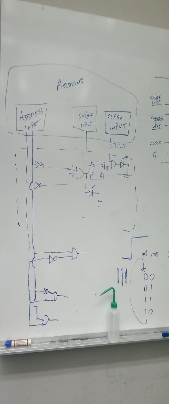
2 We had to design a Led circuit that would contain multiple Leds, activate them by address, then holds the flashing addressed Led in memory and activates another Led to blink, allowing the circuit to have multiple flashing Leds, in the final circuit there will be around a thousand Leds. This massive circuit board will be for a calorimeter, that will be use to run experiments on about a thousand crystal samples of lead tungsten at the Jefferson Lab.

3 At Jefferson lab there is a similar apparatus to the one we are trying to create. So we took a look at Thier circuit board to determine how to make ours. Their board is only able to blink one specific LED from the whole board, one sends 8 bits to the input of the board with the address of the column and the address of the LED. This way, it is not possible to blink two (or more) LEDs at the same time. We took away some good ideas, but mostly we made a original circuit.


4 There is an input where one sends a square wave to the board. The frequency of this square wave is the frequency that the LED will blink (typically 1 khz).


5 Every Circuit contains different components to perform certain tasks. In this circuit we have 4 components; not including the controller. Two-input AND gates LEDS Hex knot inverters D Flip flop


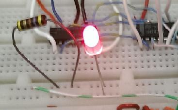
6 Light emitting diodes - is a twolead semiconductor light source. When you apply voltage to a led it emits light. When we send a binary signal of zero, there is no voltage. When we send a binary signal of one, there is a voltage So when the we produce a binary signal of one, a Led will light up.
7 A AND gate takes two inputs of binary signal 0 or 1, and produces a output based on them. If the inputs match like (1, 1), it produces a output of (1) or if the inputs are (0,0), the output is (0). If the inputs are different the output will be (0). This can be used in a variety of ways, such as setting up addresses, switches, and blinking. There is 4 of these AND Gates in the there is 8 inputs and 4 outputs

8 The hex inverter contains six inverters that invert binary signals, also know as knots. For example, if you send a binary signal of zero to the input it will out put a binary signal of one. We use this in the addressing system of the circuit, so that all the addresses produce a voltage or a binary signal of one, when addressed by the controller. Which then will cause the specific LED to light up.


9 a Flip-Flop is a circuit that has two stable states and can be used to store state information. The 7474 contains two type D flip-flops. The flip flop can be made to change state by signals applied to one or more control inputs and will have one or two outputs. It is the basic storage element in sequential logic.
 it wouldn t turn on.")
10 To make the Leds Addressable we combined the hex inverter with the 7408 two-input AND gate. The AND gate requires two binary signals of one to create a binary signal of one output, so when we tried to access the LED with the binary signal(0,0) it wouldn t turn on. To fix this we ran all the binary signals of zero through the inverter to create binary signals of one, thus turning on the LED, but only if the binary signal send was zero or else the LED remains off.
 which determines, if the Led will turn off, on or remain at its current state.")
11 The D Flip-flop gives each Led memory by being able to change the Leds state and remembering the last active state. Each time we address a Led we send a binary signal of one or zero to the flip flops input (D) which determines, if the Led will turn off, on or remain at its current state. Then if we want to turn another off or on we change the state and address another led, but those we are not addressing keep there last known state.
12 To adjust the frequency at which the LEDs blink, we simply used a AND gate. The output from the D flip-flop feed into one input while the other was hooked up to the controller which would send a square wave at specified intervals thus changing the frequency.

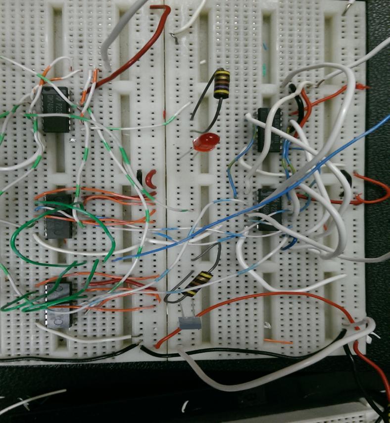
13 The protoype circuit has addressable LEDs and each led has memory so we can turn more than one on at a time and have them blink at adjustable frequencies.


14 We have chosen an Arduino Uno to be our controller and have programmed it to test the addressability of the LEDS. Also, We are working on making sub programs to do different tasks, such as all off, all on, and two at a time. In the future I hope to develop a sequence so that the LEDs light up in a given order or on command and turn off in a different order, so that the researchers can remotely turn on and off different LEDS.


15 The Arduino Uno uses the simple c programming language. Most of the programs we used can be found online but more complex ones will take time to produce from the simple examples online.


16 After we have sorted out all the bugs in the programs. we must make a full size circuit diagram for the 1000 Led board. Next we will send this diagram to a circuit board manufacturer so they can make the huge board for the apparatus that will be used to run the experiments at Jefferson Lab.

17 At the start of this project I knew nothing about circuits. Yet I was able to make this complex circuit to do exactly what we wanted. It was not easy, but this internship has been a great experiencing.

18


19 We have produced a circuit that addresses LEDs that are able to remember being addressed until readdressed and told otherwise, so that we can access each LED individually and control the frequency of they re blinks. Which is all done through our controller an Arduino Uno. That we programmed to perform the required functions.

20
LATCHES & FLIP-FLOP. Chapter 7
 LATCHES & FLIP-FLOP Chapter 7 INTRODUCTION Latch and flip flops are categorized as bistable devices which have two stable states,called SET and RESET. They can retain either of this states indefinitely
YEDITEPE UNIVERSITY DEPARTMENT OF COMPUTER ENGINEERING. EXPERIMENT VIII: FLIP-FLOPS, COUNTERS 2014 Fall
 YEDITEPE UNIVERSITY DEPARTMENT OF COMPUTER ENGINEERING EXPERIMENT VIII: FLIP-FLOPS, COUNTERS 2014 Fall Objective: - Dealing with the operation of simple sequential devices. Learning invalid condition in
The outputs are formed by a combinational logic function of the inputs to the circuit or the values stored in the flip-flops (or both).
.") 1 The outputs are formed by a combinational logic function of the inputs to the circuit or the values stored in the flip-flops (or both). The value that is stored in a flip-flop when the clock pulse occurs
1 The outputs are formed by a combinational logic function of the inputs to the circuit or the values stored in the flip-flops (or both). The value that is stored in a flip-flop when the clock pulse occurs
Digital 1 Final Project Sequential Digital System - Slot Machine
 Digital 1 Final Project Sequential Digital System - Slot Machine Joseph Messner Thomas Soistmann Alexander Dillman I. Introduction The purpose of this lab is to create a circuit that would represent the
Digital Systems Laboratory 3 Counters & Registers Time 4 hours
 Digital Systems Laboratory 3 Counters & Registers Time 4 hours Aim: To investigate the counters and registers constructed from flip-flops. Introduction: In the previous module, you have learnt D, S-R,
COMP2611: Computer Organization. Introduction to Digital Logic
 1 COMP2611: Computer Organization Sequential Logic Time 2 Till now, we have essentially ignored the issue of time. We assume digital circuits: Perform their computations instantaneously Stateless: once
To design a sequential logic circuit using D-Flip-flop. To implement the designed circuit.
 6.1 Objectives To design a sequential logic circuit using D-Flip-flop. To implement the designed circuit. 6.2 Sequential Logic So far we have implemented digital circuits whose outputs depend only on its
Introduction. Serial In - Serial Out Shift Registers (SISO)
") Introduction Shift registers are a type of sequential logic circuit, mainly for storage of digital data. They are a group of flip-flops connected in a chain so that the output from one flip-flop becomes
Introduction Shift registers are a type of sequential logic circuit, mainly for storage of digital data. They are a group of flip-flops connected in a chain so that the output from one flip-flop becomes
Name Of The Experiment: Sequential circuit design Latch, Flip-flop and Registers
 EEE 304 Experiment No. 07 Name Of The Experiment: Sequential circuit design Latch, Flip-flop and Registers Important: Submit your Prelab at the beginning of the lab. Prelab 1: Construct a S-R Latch and
D Latch (Transparent Latch)
") D Latch (Transparent Latch) -One way to eliminate the undesirable condition of the indeterminate state in the SR latch is to ensure that inputs S and R are never equal to 1 at the same time. This is done
D Latch (Transparent Latch) -One way to eliminate the undesirable condition of the indeterminate state in the SR latch is to ensure that inputs S and R are never equal to 1 at the same time. This is done
Light Emitting Diodes and Digital Circuits I
 LED s and Digital Circuits I. p. 1 Light Emitting Diodes and Digital Circuits I The Light Emitting Diode: The light emitting diode (LED) is used as a probe in the digital experiments below. We begin by
EMT 125 Digital Electronic Principles I CHAPTER 6 : FLIP-FLOP
 EMT 125 Digital Electronic Principles I CHAPTER 6 : FLIP-FLOP 1 Chapter Overview Latches Gated Latches Edge-triggered flip-flops Master-slave flip-flops Flip-flop operating characteristics Flip-flop applications
SEQUENTIAL CIRCUITS THE RELAY CIRCUIT
 SEQUENTIAL CIRCUITS THE RELAY CIRCUIT This circuit is one big circle. The main switch is open and the flexible contact is closed. Note: A closed inverter (NOT gate) circuit performs the same function.
Digital Networks and Systems Laboratory 2 Basic Digital Building Blocks Time 4 hours
 Digital Networks and Systems Laboratory 2 Basic Digital Building Blocks Time 4 hours Aim To investigate the basic digital circuit building blocks constructed from combinatorial logic or dedicated Integrated
Experiment # 9. Clock generator circuits & Counters. Digital Design LAB
 Digital Design LAB Islamic University Gaza Engineering Faculty Department of Computer Engineering Fall 2012 ECOM 2112: Digital Design LAB Eng: Ahmed M. Ayash Experiment # 9 Clock generator circuits & Counters
NEW MEXICO STATE UNIVERSITY Electrical and Computer Engineering Department. EE162 Digital Circuit Design Fall Lab 5: Latches & Flip-Flops
 NEW MEXICO STATE UNIVERSITY Electrical and Computer Engineering Department EE162 Digital Circuit Design Fall 2012 OBJECTIVES: Lab 5: Latches & Flip-Flops The objective of this lab is to examine and understand
Experiment # 4 Counters and Logic Analyzer
 EE20L - Introduction to Digital Circuits Experiment # 4. Synopsis: Experiment # 4 Counters and Logic Analyzer In this lab we will build an up-counter and a down-counter using 74LS76A - Flip Flops. The
CPSC 121: Models of Computation Lab #5: Flip-Flops and Frequency Division
 CPSC 121: Models of Computation Lab #5: Flip-Flops and Frequency Division Objectives In this lab, you will see two types of sequential circuits: latches and flip-flops. Latches and flip-flops can be used
Light Emitting Diodes and Digital Circuits I
 LED s and Digital Circuits I. p. 1 Light Emitting Diodes and Digital Circuits I Tasks marked by an asterisk (*) may be carried out before coming to the lab. The Light Emitting Diode: The light emitting
Chapter 9 MSI Logic Circuits
 Chapter 9 MSI Logic Circuits Chapter 9 Objectives Selected areas covered in this chapter: Analyzing/using decoders & encoders in circuits. Advantages and disadvantages of LEDs and LCDs. Observation/analysis
NORTHWESTERN UNIVERSITY TECHNOLOGICAL INSTITUTE
 NORTHWESTERN UNIVERSITY TECHNOLOGICL INSTITUTE ECE 270 Experiment #8 DIGITL CIRCUITS Prelab 1. Draw the truth table for the S-R Flip-Flop as shown in the textbook. Draw the truth table for Figure 7. 2.
COMP sequential logic 1 Jan. 25, 2016
 OMP 273 5 - sequential logic 1 Jan. 25, 2016 Sequential ircuits All of the circuits that I have discussed up to now are combinational digital circuits. For these circuits, each output is a logical combination
The reduction in the number of flip-flops in a sequential circuit is referred to as the state-reduction problem.
 State Reduction The reduction in the number of flip-flops in a sequential circuit is referred to as the state-reduction problem. State-reduction algorithms are concerned with procedures for reducing the
ASYNCHRONOUS COUNTER CIRCUITS
 ASYNCHRONOUS COUNTER CIRCUITS Asynchronous counters do not have a common clock that controls all the Hipflop stages. The control clock is input into the first stage, or the LSB stage of the counter. The
Light Emitting Diodes and Digital Circuits I
 LED s and Digital Circuits I. p. 1 Light Emitting Diodes and Digital Circuits I Tasks marked by an asterisk (*) may be carried out before coming to the lab. The Light Emitting Diode: The light emitting
Chapter 8 Sequential Circuits
 Philadelphia University Faculty of Information Technology Department of Computer Science Computer Logic Design By 1 Chapter 8 Sequential Circuits 1 Classification of Combinational Logic 3 Sequential circuits
Sequential Digital Design. Laboratory Manual. Experiment #3. Flip Flop Storage Elements
 The Islamic University of Gaza Engineering Faculty Department of Computer Engineering Spring 2018 ECOM 2022 Khaleel I. Shaheen Sequential Digital Design Laboratory Manual Experiment #3 Flip Flop Storage
Logic Design. Flip Flops, Registers and Counters
 Logic Design Flip Flops, Registers and Counters Introduction Combinational circuits: value of each output depends only on the values of inputs Sequential Circuits: values of outputs depend on inputs and
BISHOP ANSTEY HIGH SCHOOL & TRINITY COLLEGE EAST SIXTH FORM CXC CAPE PHYSICS, UNIT 2 Ms. S. S. CALBIO NOTES lesson #39
 BISHOP ANSTEY HIGH SCHOOL & TRINITY COLLEGE EAST SIXTH FORM CXC CAPE PHYSICS, UNIT 2 Ms. S. S. CALBIO NOTES lesson #39 Objectives: Students should be able to Thursday 21 st January 2016 @ 10:45 am Module
DEPARTMENT OF COMPUTER SCIENCE & ENGINEERING
 DRONACHARYA GROUP OF INSTITUTIONS, GREATER NOIDA Affiliated to Mahamaya Technical University, Noida Approved by AICTE DEPARTMENT OF COMPUTER SCIENCE & ENGINEERING Lab Manual for Computer Organization Lab
EKT 121/4 ELEKTRONIK DIGIT 1
 EKT 121/4 ELEKTRONIK DIGIT 1 Kolej Universiti Kejuruteraan Utara Malaysia Bistable Storage Devices and Related Devices Introduction Latches and flip-flops are the basic single-bit memory elements used
UNIVERSITY OF CALIFORNIA, DAVIS Department of Electrical and Computer Engineering. EEC180A DIGITAL SYSTEMS I Winter 2006
 UNIVERSIT OF CLIFORNI, DVIS Department of Electrical and Computer Engineering EEC180 DIGITL SSTEMS I Winter 2006 L 5: STTIC HZRDS, LTCHES ND FLIP-FLOPS The purpose of this lab is to introduce a phenomenon
CPSC 121: Models of Computation Lab #5: Flip-Flops and Frequency Division
 CPSC 121: Models of Computation Lab #5: Flip-Flops and Frequency Division Objectives In this lab, we will see the sequential circuits latches and flip-flops. Latches and flip-flops can be used to build
The word digital implies information in computers is represented by variables that take a limited number of discrete values.
 Class Overview Cover hardware operation of digital computers. First, consider the various digital components used in the organization and design. Second, go through the necessary steps to design a basic
EXPERIMENT #6 DIGITAL BASICS
 EXPERIMENT #6 DIGITL SICS Digital electronics is based on the binary number system. Instead of having signals which can vary continuously as in analog circuits, digital signals are characterized by only
(CSC-3501) Lecture 7 (07 Feb 2008) Seung-Jong Park (Jay) CSC S.J. Park. Announcement
 Lecture 7 (07 Feb 2008) Seung-Jong Park (Jay) CSC S.J. Park. Announcement") Seung-Jong Park (Jay) http://www.csc.lsu.edu/~sjpark Computer Architecture (CSC-3501) Lecture 7 (07 Feb 2008) 1 Announcement 2 1 Combinational vs. Sequential Logic Combinational Logic Memoryless Outputs
Seung-Jong Park (Jay) http://www.csc.lsu.edu/~sjpark Computer Architecture (CSC-3501) Lecture 7 (07 Feb 2008) 1 Announcement 2 1 Combinational vs. Sequential Logic Combinational Logic Memoryless Outputs
LAB #4 SEQUENTIAL LOGIC CIRCUIT
 LAB #4 SEQUENTIAL LOGIC CIRCUIT OBJECTIVES 1. To learn how basic sequential logic circuit works 2. To test and investigate the operation of various latch and flip flop circuits INTRODUCTIONS Sequential
Introduction. NAND Gate Latch. Digital Logic Design 1 FLIP-FLOP. Digital Logic Design 1
 2007 Introduction BK TP.HCM FLIP-FLOP So far we have seen Combinational Logic The output(s) depends only on the current values of the input variables Here we will look at Sequential Logic circuits The
Digital Fundamentals. Lab 5 Latches & Flip-Flops CETT Name: Date:
 Richland College School of Engineering & Technology Rev. 0 B. Donham Rev. 1 (7/2003) J. Horne Rev. 2 (1/2008) J. Bradbury Rev. 3 (7/2015) J. Bradbury Digital Fundamentals CETT 1425 Lab 5 Latches & Flip-Flops
Dr. Shahram Shirani COE2DI4 Midterm Test #2 Nov 19, 2008
 Page 1 Dr. Shahram Shirani COE2DI4 Midterm Test #2 Nov 19, 2008 Instructions: This examination paper includes 13 pages and 20 multiple-choice questions starting on page 3. You are responsible for ensuring
ECE 331 Digital System Design
 ECE 331 Digital System Design Counters (Lecture #20) The slides included herein were taken from the materials accompanying Fundamentals of Logic Design, 6 th Edition, by Roth and Kinney, and were used
Laboratory 1 - Introduction to Digital Electronics and Lab Equipment (Logic Analyzers, Digital Oscilloscope, and FPGA-based Labkit)
") Massachusetts Institute of Technology Department of Electrical Engineering and Computer Science 6. - Introductory Digital Systems Laboratory (Spring 006) Laboratory - Introduction to Digital Electronics
Massachusetts Institute of Technology Department of Electrical Engineering and Computer Science 6. - Introductory Digital Systems Laboratory (Spring 006) Laboratory - Introduction to Digital Electronics
ECE 301 Digital Electronics
 ECE 301 Digital Electronics Counters (Lecture #20) The slides included herein were taken from the materials accompanying Fundamentals of Logic Design, 6 th Edition, by Roth and Kinney, and were used with
# "$ $ # %!"$!# &!'$("!)!"! $ # *!"! $ '!!$ #!!)! $ "# ' "
!! $ # *!! $ '!!$ #!!)! $ # '") !" #!""! # "$ $ # %!"$!# &!'$("!)!"! $ # *!"! $ '!!$ #!!)! $ "# ' " % &! # Design a combinational logic circuit 10:4 encoder which has a 10-bit input (D9 to D0) and a 4-bit output. If bit position i of
!" #!""! # "$ $ # %!"$!# &!'$("!)!"! $ # *!"! $ '!!$ #!!)! $ "# ' " % &! # Design a combinational logic circuit 10:4 encoder which has a 10-bit input (D9 to D0) and a 4-bit output. If bit position i of
Chapter 6. Flip-Flops and Simple Flip-Flop Applications
 Chapter 6 Flip-Flops and Simple Flip-Flop Applications Basic bistable element It is a circuit having two stable conditions (states). It can be used to store binary symbols. J. C. Huang, 2004 Digital Logic
Laboratory 10. Required Components: Objectives. Introduction. Digital Circuits - Logic and Latching (modified from lab text by Alciatore)
") Laboratory 10 Digital Circuits - Logic and Latching (modified from lab text by Alciatore) Required Components: 1x 330 resistor 4x 1k resistor 2x 0.F capacitor 1x 2N3904 small signal transistor 1x LED 1x
Laboratory 10 Digital Circuits - Logic and Latching (modified from lab text by Alciatore) Required Components: 1x 330 resistor 4x 1k resistor 2x 0.F capacitor 1x 2N3904 small signal transistor 1x LED 1x
CSE Latches and Flip-flops Dr. Izadi. NOR gate property: A B Z Cross coupled NOR gates: S M S R Q M
 CSE-4523 Latches and Flip-flops Dr. Izadi NOR gate property: A B Z A B Z Cross coupled NOR gates: S M S R M R S M R S R S R M S S M R R S ' Gate R Gate S R S G R S R (t+) S G R Flip_flops:. S-R flip-flop
Chapter 4: One-Shots, Counters, and Clocks
 Chapter 4: One-Shots, Counters, and Clocks I. The Monostable Multivibrator (One-Shot) The timing pulse is one of the most common elements of laboratory electronics. Pulses can control logical sequences
Laboratory 7. Lab 7. Digital Circuits - Logic and Latching
 Laboratory 7 igital Circuits - Logic and Latching Required Components: 1 330 resistor 4 resistor 2 0.1 F capacitor 1 2N3904 small signal transistor 1 LE 1 7408 AN gate IC 1 7474 positive edge triggered
Engr354: Digital Logic Circuits
 Engr354: igital Circuits Chapter 7 Sequential Elements r. Curtis Nelson Sequential Elements In this chapter you will learn about: circuits that can store information; Basic cells, latches, and flip-flops;
Flip-flops, like logic gates are defined by their truth table. Flip-flops are controlled by an external clock pulse. C
 P517/617 Lec10, P1 eview from last week: Flip-Flops: asic counting unit in computer counters shift registers memory Example: S flip-flop or eset-set flip-flop Flip-flops, like logic gates are defined by
Flip-Flops and Related Devices. Wen-Hung Liao, Ph.D. 4/11/2001
 Flip-Flops and Related Devices Wen-Hung Liao, Ph.D. 4/11/2001 Objectives Recognize the various IEEE/ANSI flip-flop symbols. Use state transition diagrams to describe counter operation. Use flip-flops in
CARLETON UNIVERSITY. Facts without theory is trivia. Theory without facts is bull 2607-LRB
 CARLETON UNIVERSITY Deparment of Electronics ELEC 267 Switching Circuits February 7, 25 Facts without theory is trivia. Theory without facts is bull Anon Laboratory 3.: The T-Bird Tail-Light Control Using
Today 3/8/11 Lecture 8 Sequential Logic, Clocks, and Displays
 Today 3/8/ Lecture 8 Sequential Logic, Clocks, and Displays Flip Flops and Ripple Counters One Shots and Timers LED Displays, Decoders, and Drivers Homework XXXX Reading H&H sections on sequential logic
006 Dual Divider. Two clock/frequency dividers with reset
 006 Dual Divider Two clock/frequency dividers with reset Comments, suggestions, questions and corrections are welcomed & encouraged: contact@castlerocktronics.com 1 castlerocktronics.com Contents 3 0.
A clock is a free-running signal with a cycle time. A clock may be either high or low, and alternates between the two states.
 Clocks A clock is a free-running signal with a cycle time. A clock may be either high or low, and alternates between the two states. 1 The length of time the clock is high before changing states is its
MUHAMMAD NAEEM LATIF MCS 3 RD SEMESTER KHANEWAL
 1. A stage in a shift register consists of (a) a latch (b) a flip-flop (c) a byte of storage (d) from bits of storage 2. To serially shift a byte of data into a shift register, there must be (a) one click
Digital Design, Kyung Hee Univ. Chapter 5. Synchronous Sequential Logic
 Chapter 5. Synchronous Sequential Logic 1 5.1 Introduction Electronic products: ability to send, receive, store, retrieve, and process information in binary format Dependence on past values of inputs Sequential
The basic logic gates are the inverter (or NOT gate), the AND gate, the OR gate and the exclusive-or gate (XOR). If you put an inverter in front of
, the AND gate, the OR gate and the exclusive-or gate (XOR). If you put an inverter in front of") 1 The basic logic gates are the inverter (or NOT gate), the AND gate, the OR gate and the exclusive-or gate (XOR). If you put an inverter in front of the AND gate, you get the NAND gate etc. 2 One of the
1 The basic logic gates are the inverter (or NOT gate), the AND gate, the OR gate and the exclusive-or gate (XOR). If you put an inverter in front of the AND gate, you get the NAND gate etc. 2 One of the
EET 1131 Lab #10 Latches and Flip-Flops
 Name OBJECTIVES: 1. To study the operation of a D latch. 2. To study the operation of a D flip-flop. 3. To study the operation of a J-K flip-flop. EQUIPMENT REQUIRED: Safety glasses ICs: 7474, 7475, 74LS76
DIGITAL CIRCUIT LOGIC UNIT 9: MULTIPLEXERS, DECODERS, AND PROGRAMMABLE LOGIC DEVICES
 DIGITAL CIRCUIT LOGIC UNIT 9: MULTIPLEXERS, DECODERS, AND PROGRAMMABLE LOGIC DEVICES 1 Learning Objectives 1. Explain the function of a multiplexer. Implement a multiplexer using gates. 2. Explain the
Digital Circuits I and II Nov. 17, 1999
 Physics 623 Digital Circuits I and II Nov. 17, 1999 Digital Circuits I 1 Purpose To introduce the basic principles of digital circuitry. To understand the small signal response of various gates and circuits
Figure 30.1a Timing diagram of the divide by 60 minutes/seconds counter
 Digital Clock The timing diagram figure 30.1a shows the time interval t 6 to t 11 and t 19 to t 21. At time interval t 9 the units counter counts to 1001 (9) which is the terminal count of the 74x160 decade
Chapter. Synchronous Sequential Circuits
 Chapter 5 Synchronous Sequential Circuits Logic Circuits- Review Logic Circuits 2 Combinational Circuits Consists of logic gates whose outputs are determined from the current combination of inputs. Performs
FLIP-FLOPS AND RELATED DEVICES
 C H A P T E R 5 FLIP-FLOPS AND RELATED DEVICES OUTLINE 5- NAND Gate Latch 5-2 NOR Gate Latch 5-3 Troubleshooting Case Study 5-4 Digital Pulses 5-5 Clock Signals and Clocked Flip-Flops 5-6 Clocked S-R Flip-Flop
Part 4: Introduction to Sequential Logic. Basic Sequential structure. Positive-edge-triggered D flip-flop. Flip-flops classified by inputs
 Part 4: Introduction to Sequential Logic Basic Sequential structure There are two kinds of components in a sequential circuit: () combinational blocks (2) storage elements Combinational blocks provide
Synchronous Sequential Logic
 Synchronous Sequential Logic -A Sequential Circuit consists of a combinational circuit to which storage elements are connected to form a feedback path. The storage elements are devices capable of storing
Lesson 12. Advanced Digital Integrated Circuits Flip-Flops, Counters, Decoders, Displays
 Lesson 12 Sierra College CIE-01 Jim Weir 530.272.2203 jweir43@gmail.com www.rstengineering.com/sierra Advanced Digital Integrated Circuits Flip-Flops, Counters, Decoders, Displays Flip-Flops: True name
Introduction to Microprocessor & Digital Logic
 ME262 Introduction to Microprocessor & Digital Logic (Sequential Logic) Summer 2 Sequential Logic Definition The output(s) of a sequential circuit depends d on the current and past states of the inputs,
Logic. Andrew Mark Allen March 4, 2012
 Logic Andrew Mark Allen - 05370299 March 4, 2012 Abstract NAND gates and inverters were used to construct several different logic gates whose operations were investigate under various inputs. Then the
Contents Circuits... 1
 Contents Circuits... 1 Categories of Circuits... 1 Description of the operations of circuits... 2 Classification of Combinational Logic... 2 1. Adder... 3 2. Decoder:... 3 Memory Address Decoder... 5 Encoder...
1. Convert the decimal number to binary, octal, and hexadecimal.
 1. Convert the decimal number 435.64 to binary, octal, and hexadecimal. 2. Part A. Convert the circuit below into NAND gates. Insert or remove inverters as necessary. Part B. What is the propagation delay
Multiplexor (aka MUX) An example, yet VERY useful circuit!
 An example, yet VERY useful circuit!") Multiplexor (aka MUX) An example, yet VERY useful circuit! A B 0 1 Y S A B Y 0 0 x 0 0 1 x 1 1 x 0 0 1 x 1 1 S=1 S=0 Y = (S)? B:A; Y=S A+SB when S = 0: output A 1: output B 56 A 32-bit MUX Use 32 1-bit
Multiplexor (aka MUX) An example, yet VERY useful circuit! A B 0 1 Y S A B Y 0 0 x 0 0 1 x 1 1 x 0 0 1 x 1 1 S=1 S=0 Y = (S)? B:A; Y=S A+SB when S = 0: output A 1: output B 56 A 32-bit MUX Use 32 1-bit
Introduction to Digital Electronics
 Introduction to Digital Electronics by Agner Fog, 2018-10-15. Contents 1. Number systems... 3 1.1. Decimal, binary, and hexadecimal numbers... 3 1.2. Conversion from another number system to decimal...
Lecture 8: Sequential Logic
 Lecture 8: Sequential Logic Last lecture discussed how we can use digital electronics to do combinatorial logic we designed circuits that gave an immediate output when presented with a given set of inputs
DIGITAL CIRCUIT COMBINATORIAL LOGIC
 DIGITAL CIRCUIT COMBINATORIAL LOGIC Logic levels: one zero true false high low CMOS logic levels: 1 => 0.7 V DD 0.4 V DD = noise margin 0 =< 0.3 V DD Positive logic: high = 1 = true low = 0 = false Negative
ELECTRICAL ENGINEERING DEPARTMENT California Polytechnic State University
 EECTRICA ENGINEERING DEPARTMENT California Polytechnic State University EE 361 NAND ogic Gate, RS Flip-Flop & JK Flip-Flop Pre-lab 7 1. Draw the logic symbol and construct the truth table for a NAND gate.
Name: Date: Suggested Reading Chapter 7, Digital Systems, Principals and Applications; Tocci
 Richland College Engineering Technology Rev. 0 B. Donham Rev. 1 (7/2003) J. Horne Rev. 2 (1/2008) J. Bradbury Digital Fundamentals CETT 1425 Lab 7 Asynchronous Ripple Counters Name: Date: Objectives: To
Chapter 7 Memory and Programmable Logic
 EEA091 - Digital Logic 數位邏輯 Chapter 7 Memory and Programmable Logic 吳俊興國立高雄大學資訊工程學系 2006 Chapter 7 Memory and Programmable Logic 7-1 Introduction 7-2 Random-Access Memory 7-3 Memory Decoding 7-4 Error
6.3 Sequential Circuits (plus a few Combinational)
") 6.3 Sequential Circuits (plus a few Combinational) Logic Gates: Fundamental Building Blocks Introduction to Computer Science Robert Sedgewick and Kevin Wayne Copyright 2005 http://www.cs.princeton.edu/introcs
6.3 Sequential Circuits (plus a few Combinational) Logic Gates: Fundamental Building Blocks Introduction to Computer Science Robert Sedgewick and Kevin Wayne Copyright 2005 http://www.cs.princeton.edu/introcs
Sequential Logic and Clocked Circuits
 Sequential Logic and Clocked Circuits Clock or Timing Device Input Variables State or Memory Element Combinational Logic Elements From combinational logic, we move on to sequential logic. Sequential logic
DIGITAL SYSTEM FUNDAMENTALS (ECE421) DIGITAL ELECTRONICS FUNDAMENTAL (ECE422) LATCHES and FLIP-FLOPS
 DIGITAL ELECTRONICS FUNDAMENTAL (ECE422) LATCHES and FLIP-FLOPS") COURSE / CODE DIGITAL SYSTEM FUNDAMENTALS (ECE421) DIGITAL ELECTRONICS FUNDAMENTAL (ECE422) LATCHES and FLIP-FLOPS In the same way that logic gates are the building blocks of combinatorial circuits, latches
COURSE / CODE DIGITAL SYSTEM FUNDAMENTALS (ECE421) DIGITAL ELECTRONICS FUNDAMENTAL (ECE422) LATCHES and FLIP-FLOPS In the same way that logic gates are the building blocks of combinatorial circuits, latches
Asynchronous (Ripple) Counters
 Counters") Circuits for counting events are frequently used in computers and other digital systems. Since a counter circuit must remember its past states, it has to possess memory. The chapter about flip-flops introduced
Circuits for counting events are frequently used in computers and other digital systems. Since a counter circuit must remember its past states, it has to possess memory. The chapter about flip-flops introduced
Exercise 2: Connecting the Digital Logic Circuits
 Exercise 2: Connecting the Digital Logic Circuits EXERCISE OBJECTIVE When you have completed this exercise, you will be able to connect digital logic circuits and observe the inputs and outputs by using
Reaction Game Kit MitchElectronics 2019
 Reaction Game Kit MitchElectronics 2019 www.mitchelectronics.co.uk CONTENTS Schematic 3 How It Works 4 Materials 6 Construction 8 Important Information 9 Page 2 SCHEMATIC Page 3 SCHEMATIC EXPLANATION The
RS flip-flop using NOR gate
 RS flip-flop using NOR gate Triggering and triggering methods Triggering : Applying train of pulses, to set or reset the memory cell is known as Triggering. Triggering methods:- There are basically two
Computer Science 324 Computer Architecture Mount Holyoke College Fall Topic Notes: Sequential Circuits
 Computer Science 324 Computer Architecture Mount Holyoke College Fall 2009 opic Notes: Sequential Circuits Let s think about how life can be bad for a circuit. Edge Detection Consider this one: What is
Chapter 5 Flip-Flops and Related Devices
 Chapter 5 Flip-Flops and Related Devices Chapter 5 Objectives Selected areas covered in this chapter: Constructing/analyzing operation of latch flip-flops made from NAND or NOR gates. Differences of synchronous/asynchronous
CHAPTER 4: Logic Circuits
 CHAPTER 4: Logic Circuits II. Sequential Circuits Combinational circuits o The outputs depend only on the current input values o It uses only logic gates, decoders, multiplexers, ALUs Sequential circuits
DIGITAL ELECTRONICS: LOGIC AND CLOCKS
 DIGITL ELECTRONICS: LOGIC ND CLOCKS L 6 INTRO: INTRODUCTION TO DISCRETE DIGITL LOGIC, MEMORY, ND CLOCKS GOLS In this experiment, we will learn about the most basic elements of digital electronics, from
EET2411 DIGITAL ELECTRONICS
 5-8 Clocked D Flip-FlopFlop One data input. The output changes to the value of the input at either the positive going or negative going clock trigger. May be implemented with a J-K FF by tying the J input
Introduction to Sequential Circuits
 Introduction to Sequential Circuits COE 202 Digital Logic Design Dr. Muhamed Mudawar King Fahd University of Petroleum and Minerals Presentation Outline Introduction to Sequential Circuits Synchronous
PRE J. Figure 25.1a J-K flip-flop with Asynchronous Preset and Clear inputs
 Asynchronous Preset and Clear Inputs The S-R, J-K and D inputs are known as synchronous inputs because the outputs change when appropriate input values are applied at the inputs and a clock signal is applied
Unit 11. Latches and Flip-Flops
 Unit 11 Latches and Flip-Flops 1 Combinational Circuits A combinational circuit consists of logic gates whose outputs, at any time, are determined by combining the values of the inputs. For n input variables,
Design of a Binary Number Lock (using schematic entry method) 1. Synopsis: 2. Description of the Circuit:
 1. Synopsis: 2. Description of the Circuit:") Design of a Binary Number Lock (using schematic entry method) 1. Synopsis: This lab gives you more exercise in schematic entry, state machine design using the one-hot state method, further understanding
Design of a Binary Number Lock (using schematic entry method) 1. Synopsis: This lab gives you more exercise in schematic entry, state machine design using the one-hot state method, further understanding
MODULAR DIGITAL ELECTRONICS TRAINING SYSTEM
 MODULAR DIGITAL ELECTRONICS TRAINING SYSTEM MDETS UCTECH's Modular Digital Electronics Training System is a modular course covering the fundamentals, concepts, theory and applications of digital electronics.
Computer Organization & Architecture Lecture #5
 Computer Organization & Architecture Lecture #5 Shift Register A shift register is a register in which binary data can be stored and then shifted left or right when a shift signal is applied. Bits shifted
1. True/False Questions (10 x 1p each = 10p) (a) I forgot to write down my name and student ID number.
 (a) I forgot to write down my name and student ID number.") CprE 281: Digital Logic Midterm 2: Friday Oct 30, 2015 Student Name: Student ID Number: Lab Section: Mon 9-12(N) Mon 12-3(P) Mon 5-8(R) Tue 11-2(U) (circle one) Tue 2-5(M) Wed 8-11(J) Wed 6-9(Y) Thur 11-2(Q)
CprE 281: Digital Logic Midterm 2: Friday Oct 30, 2015 Student Name: Student ID Number: Lab Section: Mon 9-12(N) Mon 12-3(P) Mon 5-8(R) Tue 11-2(U) (circle one) Tue 2-5(M) Wed 8-11(J) Wed 6-9(Y) Thur 11-2(Q)
Chapter 4. Logic Design
 Chapter 4 Logic Design 4.1 Introduction. In previous Chapter we studied gates and combinational circuits, which made by gates (AND, OR, NOT etc.). That can be represented by circuit diagram, truth table
ELCT201: DIGITAL LOGIC DESIGN
 ELCT201: DIGITAL LOGIC DESIGN Dr. Eng. Haitham Omran, haitham.omran@guc.edu.eg Dr. Eng. Wassim Alexan, wassim.joseph@guc.edu.eg Lecture 6 Following the slides of Dr. Ahmed H. Madian ذو الحجة 1438 ه Winter