MEMS / MOEMS. Stand und Perspektiven
|
|
|
- Penelope Stephens
- 6 years ago
- Views:
Transcription
1 MEMS / MOEMS Stand und Perspektiven Hubert Lakner Institute for Photonic Microsystems (IPMS Dresden) Technische Universität Dresden Prof. for Optoelectronic Devices and Systems
2 IPMS-Budget (in Mio ) 25 FhG Basic Funding 20 Public Projects Industrial Projects
3 Das IPMS Photonische Mikrosysteme für neue Anwendu Hubert Lakner


4 Schwerpunkt 2006/07: Erweiterung des IPMS Erweiterung Institutsgebäude Institutsgebäude von Süd 1992 übernimmt das IMS Neuer Reinraum 50% eines Laborgebäudes und 40% eines Reinraums des ZMD

5 Einweihung des neuen Reinraums am 10. Sept Quadratmeter 150-mm-Siliziumwafer Neuer Reinraum mit Übergang zum Institutsgebäude
6 Customer specific product development Spatial Light Modulators for Leading Edge Mask and Direct Writing in Semiconductor Microlithography (Micronic Laser Systems, ASML) Microscanners (1D and 2D) for Bar Code / Matrix Code Reading and Projection Displays (Intermec, Microvision) Organic Light Emitting Diodes for Displays and Lighting (Novaled AG, OSRAM, PHILIPS)


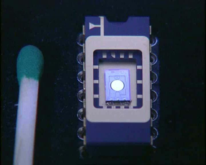
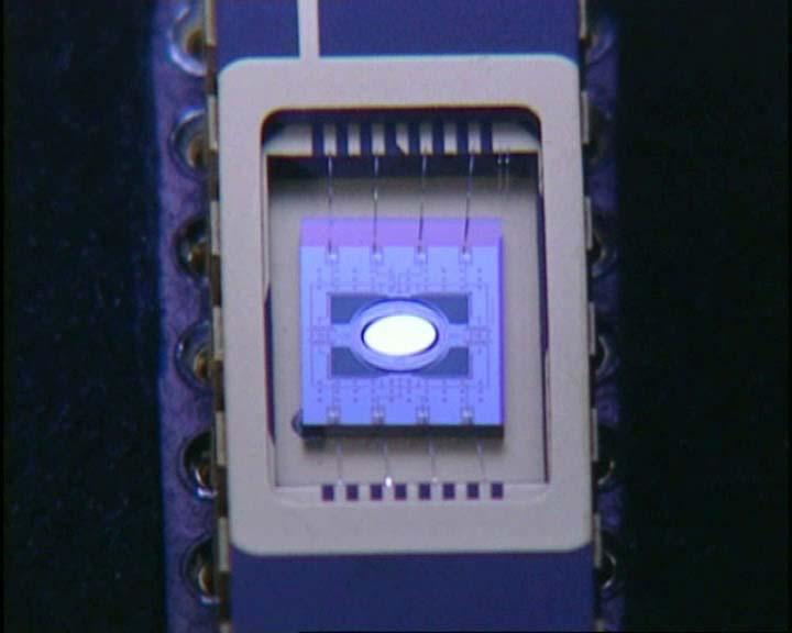
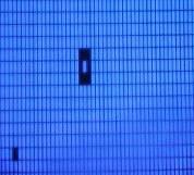
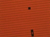
7 Spatial Light Modulator Chip The SLM chip with 1 million analog mirrors developed by the Institute of Photonic Micro Systems IPMS Active area: 33x8mm x 512 mirrors 16 microns pixel pitch 2 khz frame rate
 sacrificial layer stopper photoresist mirror silicon silicon")

8 Process Flow for the Micro-Mirrors planarization metal substrate (containing CMOS circuitry) sacrificial layer stopper photoresist mirror silicon silicon oxide U address photoresist aluminium dicing debris photoresist finished device with one deflected mirror address electrode mirror electrode counter electrode
9 Optische Funktionsprinzipien Dynamisches Beugungsgitter mit 16 Mikrometer Pixeln: IPMS chip Ausgelenkte Spiegel WLI-Aufnahme


10 The Technology - SLM Writer Micro-stepper with a programmable mask Flash on the fly


11 Sigma Laser Writing tool for 248nm DUV Key specs for mask making: Minimum Feature: 320 nm Assist features: 140 nm CD uniformity: 5 nm Address Grid: 1.6 nm SLM size: 512 x 2048 Flash rate: 2 khz Number of passes: nm L/S 180 nm L/S 140 nm L/S

12 Principle of mask and direct writing
13 Pixel calibration The pixels have non-linear voltage-to-brightness characteristics They have individual transfer functions The transfer functions are measured and stored in a huge look-up table that is accessed in real time geometry data 6 bit deep bitmap gray value map of pixel transfer functions DAC value DAC Mirror voltage SLM


14 Calibration result Before calibration After calibration


15 2-level Aktuatoren mit TiAl Feder und separater Spiegelplatte Variante mit Joch in der Federebene Kraftangriff am Joch: keine Spiegeldeformation Variante mit Knochenförmiger Feder Kraftangriff am Spiegel
16 Eigenschaften der 2-Ebenen Aktuatoren Test der Stabilität der Auslenkung (30 min) Drift: <1nm/30min Deflection [nm] Design parameters TiAl spring: 200nm Gap: 770nm Time [min]
17 Benefits of the SLM Lithography Systems Much faster than E-beam writers by using 1 million mirrors Less sensitive to electro magnetic interference Fast prototyping and higher throughput Reduced costs The present mask writing tool is used by INTEL for making PSM masks down to the 45nm technology node Future SLMs for direct writing on wafers will be developed (target: 8 million pixels, 7 micrometer pixel pitch, 8 khz puls repetition/frame rate, shorter wavelenghts 193nm)


18 Wave Front Correction for Adaptive Optics Goal: High-Resolution High-Precision High-Speed Optical Phase Control


19 Schematic of AO Wavefront Correction Goal: Real-Time Compensation of Dynamic Higher Order Wavefront Distortions


20 Applications Imaging Enhancement through Inhomogeneous or Turbulent Media Astronomy: Atmospheric Turbulence Compensation Ophtalmology: Eye Aberration Correction Microscopy: In-vivo Imaging through Biological Tissue Ultra fast Laser Pulse Shaping Free Space Optical Data Communication General Needs: High-speed, high-resolution optical phase control Formation of arbitrary spatial phase patterns with highest possible fidelity


21 Adaptive Optics Mirror Architecture


22 Measured Deflection of 40 μm Piston Mirrors Piston MMA surface 300 nm deflection Deflection Characteristic Measurement: Wyko NT 2000 White Light Interferometer Arbitrary Line Scan


23 MEMS Phase Former Kit CMOS integrated 240 x 200 Micro Mirror Array Driving board with high-speed FireWire Interfa Driver software for Windows XP based PC


")
 with 10 μm")

")
24 AO Demonstration System and Testbed Imaged USAF test chart a) undisturbed b) with 10 μm PtV aberration Top view photograph c) with modulo 2π correction (18 nm)


25 Aberration Measurement Objective, spatially and temporally resolved measurement of the eye using many hundreds of data points individual map of all refractive errors (OPD pattern) data for a personalized treatment & preview system


26 Correction of an Complex Eye Aberration Uncorrected RMS = 293 nm Corrected RMS = 47 nm

27 Femtosecond Laser Pulse Shaping Transmissive with LC-SLM Grating Incoming pulse Lens Phase-Modulator In Fourier-Plane Outgoing pulse Lens Grating Pulse spectra Reflective with MEMS-SLM Spectral decomposition Grating Lens Phase adjustment of each spectral component MEMS Phase-Modulator Superposition of modified pulse after M. Hacker, Universität Jena, IOQ

28 Examples of Pulse Shaping Pulse Compression Input Optimized phase pattern Output arbitrary compressed pulse fs-pulse THz Pulse Train Generation Input Sinusoidal phase pattern Output fs-pulse pulse train Animation:


29 Microscanners made from BSOI Wafers MicroScanningMirror 1 mm
30 Fabrication Process starting material highly doped BSOI-wafer with 30 um SOI fabrication insulation trenches fabrication metal lanes/pads backside module I aluminization, 80 nm Al backside module II etch of trenches (ASE) silicon silicon oxide aluminium silicon nitride
31
32


33 Barcode Scan Engine MIRAGE

34 Scanning Mirror Display
35 RGB-Projektionsdisplay
36 Micro Laser Camera: Endoscopy Chip Size: 2900 μm x 2350 μm Mirror: Ø 500 μm Display Light sources 500µm R G B PC Scan control Control Digitizer R G B Single mode illumination fiber Scanner Multi mode collection fiber Detectors Fixed mirror Subject


37 Endoscopy Source: Microvision Scan-Head: 8 mm diameter, SVGA resolution, full colour


38 Scanning Mirror Spectrometer NIR spectrometer scan range nm 18 nm FWHM detector signal / a. u. 0,5 NIR diode with 1300 nm NIR diode with 1550 nm 0,4 NIR diode with 1450 nm 0,3 0,2 0,1 0, wavelength / nm


39 Z- deflection for dynamic optical path length variation for dynamic focus & FTIR spectrometers 1,0 transmission spectrum polystyrene t = 1.5 mm 0,8 0,6 0,4 0,2 0,0 MEMS based FT-Spectrometer, average of 500 scans reference Nicolet Nexus 870 res. 2cm wavelength / nm transmission

40 FTIR Spectrometer with dynamic mirror MEMS mirror TE-cooled MCT detector Optical bench: 100 x 60 x 30 mm 3 Scan range: 2 5 μm Resolution 30 cm -1 Time resolved measurements possible Small Portable
41 Summary, conclusions, and outlook Photonic microsystems or MOEMS (MicroOptoElectroMechanical Systems) enable new and innovative product developments. The production gap must be closed. More and more products reach the market: MOEMS-Displays, bar code readers, SLMs for lithography, Microspectrometers, Scanners and Imagers, OLED displays and white light sources. Prognosted Growth Rates are in the range of 15% to 20% annually.


42 Center for Organic Materials and Electronic Devices Dresden
43 Mission of COMEDD Customer and Application Specific Research, Development and Pilotfabrication on novel device concepts and manufacturing methods in the field of organic materials (small molecule) Integration technologies for novel devices concepts Fabrication technologies based on innovative equipment concepts for rigid as flexible substrates New product developments including prototyping and first pilot approval Technology Development and Transfer Leading research and development center in Europe for small-molecule organic technology
 transparent conductor (ITO) organic layers organic layers metal cathode")
44 OLED: substrate emitter vs. inverted structure Light emission _ Light emission + + _ glass substrate transparent conductor (ITO) transparent conductor (ITO) organic layers organic layers metal cathode metal cathode glass substrate Inverted Structure Inverted emitter: - important for intransparent substrate - difficulty: work function control of contacts


45 Small Molecule vs. Polymers Small-Molecules Polymer Technology: Evaporation Technology: Spin-On/Ink-Jet Source: Covion
 Lowest voltages reported in literature")
![for small-molecule devices Luminance [cd/m 2 ] 10 4 10,000 cd/m 2 @5.](/docs-images/75/71818029/images/46-1.jpg "2V 10 3 1,000 cd/m 2 @2.9V 10 2 100 cd/m 2 @2.")
46 p-i-n-oled 10 5 N-doping: Batho-Phenanthroline doped with Li Current efficiency: 5.27 (pure Alq3 emitter) Lowest voltages reported in literature for small-molecule devices Luminance [cd/m 2 ] ,000 cd/m ,000 cd/m cd/m Voltage [V]


47 Optical Organic based markets First wave Second wave Third wave Lighting/Signage Solar cell Displays OLED Microdisplays OLED Optoelectronic Source: Samsung, Kodak, GE, Philips Lighting


48 COMEDD Working areas OLED Signage and Lighting Rigid Substrates Flexible Substrates Organic based MOEMS OLED on CMOS integration OLED + MEMS Organic Solarcells Rigid Substrates Flexible Substrates
49 LED vs. OLED Source: Osram OS LED Point source High Peak brightness High efficiency Long lifetime Loss for area distribution high OLED Area source Low Peak brightness High efficiency Lifetime to be improved Low loss for area distribution

50 Applications OLED-on-CMOS Microdisplay viewfinder, projection, HMD, optical inspection,... Bi-directional microdisplay OLED + optical feedback via internal CMOS sensor Light barriers Opto-coupler Optical sensors e.g. chemical, medical (fluorescence, photoplethysmography,...) Communication chip-to-chip, board-to-board, chip-to board,...

51 OLED requirements for Bi-directional Displays Deckelektrode Met1 Organik / OLED Met4 Met3 Met2 FOX FOX FOX PMOS Passivierung (Photolack) OLED requirements Met3 Met2 - High brightness > 5000 cd/m² Met1 - High efficiency > 15 lm/w Poly - High transparency > 70% - Low Voltage < 5 V - Long lifetime > 5000 hr. - Good integration possibility P-Sub Photodiode Met3 Met2 Met1
52 Dresden The heart of OLED technology R&D Materials OLED-Technol. Tools Products Modeling Industry 2008: more than 300 people altogether VON ARDENNE


53 13N8857 Signage applications 100x50 mm signage OLED on PCB signage 100x100 mm signage OLED on metal foil


54 Concepts for White lighting


55 Lighting applications OLED on ZAO Large area lighting

56 Lighting applications
57 TOLED(Transparent OLED) Orange PIN OLED and transparency Encapsulation glass Transmittance in visible range ( nm) : 69,69 % Transmittance 100 ITO... Organic stack ITO Glass substrate Transmittance (%) Wavelength (nm)

58 Transparent OLED Signage


59 OLED on CMOS 30μm 16SV /1733
60 Results: OLED emission spectra (Microstructed substrate) 1,0 1,0 blue emitter (SRmax=47.4e 3 W/m sr nm; L= Cd/m ) 0,9 Standardised Luminance L/Lmax [1] 0,8 0,6 0,4 0,2 red emitter/tin electrode (V=3.75V; Lmax=22.0 Cd/m²) green emitter/tin electrode (V=3.25V; Lmax=108.9 Cd/m²) blue emitter/tin electreode (V=6.00V; Lmax=477.6 Cd/m²) 0, Viewing angle? [ ] Red 100 cd/m² 4.8 V *) Standardised spectral radiance [1] 0,8 0,7 0,6 0,5 0,4 0,3 0,2 0,1 0,0 Colour coordinate (CIE 1931) (0.68, 0.31) Wavelenght λ [nm] Normalized spectral radiances Maximum spectral Green 3.2 V *) (0.30, 0.63) 527 nm Blue 4.4 V *) (0.14, 0.09) 452 nm Orange Luminance versus viewing angle 2.6 V (0.63, 0.36) 639 nm 613 nm *) not optimized

 Infrastructure Measurement Sublimation Testing equipment Total investment")
61 Planned Fabrication Infrastructure Cleanroom 900 m² class 10 Fabrication lines Gen2 Fabrication line 8 inch MOEMS line Roll-to-Roll Line Worldwide first vertical In-Line Fabrication System (Applied Materials) OLED cluster for Top Emission (Sunic) Infrastructure Measurement Sublimation Testing equipment Total investment 30 Mio. Euro
62 COMEDD Production facilities - Planning Prototype line Rigid substrates Pilot line Rigid/Flexible substrates Pilot line OLED-on-CMOS Roll-to-Roll Substrate size 200x200 mm² 370 x 470 mm² (Generation 2) Substrate type Glass Glass or laminated foil 150, 200 mm diameter Silicon/CMOS wafer Cycle time 120 minutes 3 minutes 60 minutes mm width Metall foil Pilot max. volume substrates/year Pilot max. volume area Prototype/ technology research and development - 80, ,000 m² - - Ready Q4/2008 Ready Q4/2008 Pilot production - Q1/2009 Q2/2008 -
63 Core Lighting Fabrication Tool (Gen2) masks masks masks masks Cleaning Loading Treatment Aixtron Module (OVPD) Organic Module I Organic Module II Metal Module Unloading Encapsulation AM.1-12 OM.I.1-3 OM.II.1-3 MM.1-2 Modular and fully automated system Pre-Treatment by plasma 1 module Organic layer technology OVPD (Organic Vapour Phase Deposition) 1 module (up to 6 layers*) VTE (Vacuum Thermal Evaporation) 5 modules (up to 6 layers*) Metal layer 2 modules e.g. Aluminium and Silver *Including dopand and host material
 2 evaporators for metals 1 DC/RF magnetron")
64 Roll-to-Roll Coater for Metal Strip Batch type Roll-to-Roll Coater substrate width 300 mm, thickness mm Pretreatment by ion beam and heating Coating Stations: up to 9 novel linear evaporators for organic materials in total (5 double, 4 single) 2 evaporators for metals 1 DC/RF magnetron OLED-specific substrate handling strip guidance w/o front side roller contact un/rewinding with plastic liner transfer of coated substrate under inert atmosphere ion beam retreatment substrate and Liner unwinding Substrate and liner rewinding organic material Evaporation sources magnetron Metal Evaporation sources
65 Conclusion In organic technologies the display market segment is only the first wave of technology The new market segments offers great opportunities for further market grow The IPMS center wants to be the leading research institute for small-molecule photonic organic technologies in Europe

66
PROCESS TECHNOLOGIES FOR ADVANCED ORGANIC ELECTRONIC DEVICES: MICRODISPLAYS, LIGHTING AND SOLAR CELLS
 PROCESS TECHNOLOGIES FOR ADVANCED ORGANIC ELECTRONIC DEVICES: MICRODISPLAYS, LIGHTING AND SOLAR CELLS Dr. Christian May Fraunhofer IPMS - Center for Organic Materials and Electronic Devices Dresden COMEDD
Advanced Sensor Technologies
 Advanced Sensor Technologies Jörg Amelung Fraunhofer Institute for Photonics Microsystems Name of presenter date Sensors as core element for IoT Next phase of market grow New/Advanced Requirements based
MEMS Technologies Dresden - Product Development and Fabrication at IPMS Dresden
 MEMS Technologies Dresden - Product Development and Fabrication at IPMS Dresden MEMS Technologies Dresden - Product Development and Fabrication at IPMS Dresden Michael Müller, Matthias List Outline FhG-IPMS
An Overview of OLED Display Technology
 page:1 An Overview of OLED Display Technology Homer Antoniadis OSRAM Opto Semiconductors Inc. San Jose, CA page:2 Outline! OLED device structure and operation! OLED materials (polymers and small molecules)!
Press Release Plastic Electronics 2013 October 8th 10th, 2013, in Dresden/Germany Hall 2, booth no. 292 (joint booth of Organic Electronic Saxony)
") Press Release Plastic Electronics 2013 October 8th 10th, 2013, in Dresden/Germany Hall 2, booth no. 292 (joint booth of Organic Electronic Saxony) Flexible OLED from the roll Tridonic Dresden and Fraunhofer
Press Release Plastic Electronics 2013 October 8th 10th, 2013, in Dresden/Germany Hall 2, booth no. 292 (joint booth of Organic Electronic Saxony) Flexible OLED from the roll Tridonic Dresden and Fraunhofer
The Company. A leading OLED player
 The Company A leading OLED player Novaled is the company to trade with, work for and invest in. Our company focuses on proprietary organic materials and complementary innovative technologies for superior
center for organic materials and electronic devices dresden
 F R A U N H O F E R I N S T I T U T e F o R P h o t o n i c M i c r o S y s t e m s I P M S center for organic materials and electronic devices dresden p r e f a c e Dr. Christian May Head of Business
Flexible Electronics Production Deployment on FPD Standards: Plastic Displays & Integrated Circuits. Stanislav Loboda R&D engineer
 Flexible Electronics Production Deployment on FPD Standards: Plastic Displays & Integrated Circuits Stanislav Loboda R&D engineer The world-first small-volume contract manufacturing for plastic TFT-arrays
Spatial Light Modulators XY Series
 Spatial Light Modulators XY Series Phase and Amplitude 512x512 and 256x256 A spatial light modulator (SLM) is an electrically programmable device that modulates light according to a fixed spatial (pixel)
P I SCALE Creating an Open Access Flexible O L E D P ilo t L in e S e r vic e
 P I SCALE Creating an Open Access Flexible O L E D P ilo t L in e S e r vic e Pavel Kudlacek pavel.kudlacek@tno.nl P I - SCALE for 2017Flex 1 Lighting c h a lle n g e L ig h t in g c h a lle n g e At least
PUBLISHABLE Summary To provide OLED stacks with improved reliability Provide improved thin film encapsulation
 PUBLISHABLE Summary SCOOP is a European funded project (FP7 project number 287595 SCOOP). It is focused on OLED technology, microdisplays based on the combination of OLED with CMOS technology, and innovative
SPATIAL LIGHT MODULATORS
 SPATIAL LIGHT MODULATORS Reflective XY Series Phase and Amplitude 512x512 A spatial light modulator (SLM) is an electrically programmable device that modulates light according to a fixed spatial (pixel)
Development of OLED Lighting Applications Using Phosphorescent Emission System
 Development of OLED Lighting Applications Using Phosphorescent Emission System Kazuhiro Oikawa R&D Department OLED Lighting Business Center KONICA MINOLTA ADVANCED LAYERS, INC. October 10, 2012 Outline
Phosphorescent OLED Technologies: The Next Wave. Plastic Electronics Conference Oct 9, 2012
 Phosphorescent OLED Technologies: The Next Wave Plastic Electronics Conference Oct 9, 2012 UDC Company Focus IP innovator, technology developer, patent licensor and materials supplier for the rapidly growing
Scalable self-aligned active matrix IGZO TFT backplane technology and its use in flexible semi-transparent image sensors. Albert van Breemen
 Scalable self-aligned active matrix IGZO TFT backplane technology and its use in flexible semi-transparent image sensors Albert van Breemen Image sensors today 1 Dominated by silicon based technology on
ORGANIC ELECTRONICS PROCESS DEVELOPMENT AND ENCAPSULATION TECHNOLOGIES
 FRAUNHOFER INSTITUTE FOR ORGANIC ELECTRONICS, ELECTRON BEAM AND PLASMA TECHNOLOGY FEP ORGANIC ELECTRONICS PROCESS DEVELOPMENT AND ENCAPSULATION TECHNOLOGIES 2 PROFILE Fraunhofer FEP combines research and
:: Reduce needs for heat dissipation components. :: Extend battery life in mobile products. :: Save power and reduce heat generation in TVs
 UniversalPHOLED Technology and Materials UniversalPHOLED Phosphorescent OLED technology and materials offer record-breaking performance to bring competitive advantages to your OLED display and lighting
Screen investigations for low energetic electron beams at PITZ
 1 Screen investigations for low energetic electron beams at PITZ S. Rimjaem, J. Bähr, H.J. Grabosch, M. Groß Contents Review of PITZ setup Screens and beam profile monitors at PITZ Test results Summary
OLED Technology Introduction
 OLED Technology Introduction An organic light emitting diode (OLED) consists of several semiconducting organic layers sandwiched between two electrodes at least one of them being transparent. A simplified
Advances in Roll-to-Roll Imprint Lithography for Display Applications Using Self Aligned Imprint Lithography. John G Maltabes HP Labs
 Advances in Roll-to-Roll Imprint Lithography for Display Applications Using Self Aligned Imprint Lithography John G Maltabes HP Labs Outline Introduction Roll to Roll Challenges and Benefits HP Labs Roll
[1.9] AMOLED 공정 Introduction OLED Materials Patterning Process Process Equipments
![[1.9] AMOLED 공정 Introduction OLED Materials Patterning Process Process Equipments](/thumbs/73/69073032.jpg "[1.9] AMOLED 공정 Introduction OLED Materials Patterning Process Process Equipments") [1.9] AMOLED 공정 1.9.1. Introduction 1.9.2. OLED Materials 1.9.3. Patterning Process 1.9.4. Process Equipments OLED : Organic Light Emitting Diode Organic EL : Organic Electroluminescent 재료및공정 재료의발광메카니즘
[1.9] AMOLED 공정 1.9.1. Introduction 1.9.2. OLED Materials 1.9.3. Patterning Process 1.9.4. Process Equipments OLED : Organic Light Emitting Diode Organic EL : Organic Electroluminescent 재료및공정 재료의발광메카니즘
Organic light emitting diodes for display technology
 Organic light emitting diodes for display technology Shamna Shamsudeen MScTI - ZITI-Heidelberg University OLED ZITI, Uni Heidelberg Page1 What s Light Light: Visible part of EM spectra. Ref:[1] Thermoluminescence:
 Page 1 of 8 Main > Electronics > Computers How OLEDs Work by Craig Freudenrich, Ph.D. Introduction to How OLEDs Work Imagine having a high-definition TV that is 80 inches wide and less than a quarter-inch
AIXTRON in EXCILIGHT project
 AIXTRON SE AIXTRON in EXCILIGHT project Gintautas Simkus ABOUT AIXTRON 2 Who we are Headquarter based in Herzogenrath, Germany Worldwide presence with 14 sales/representatives offices and production facilities
Development of OLED Lighting Panel with World-class Practical Performance
 72 Development of OLED Lighting Panel with World-class Practical Performance TAKAMURA MAKOTO *1 TANAKA JUNICHI *2 MORIMOTO MITSURU *2 MORI KOICHI *3 HORI KEIICHI *4 MUSHA MASANORI *5 Using its proprietary
Industrial Inline Control for Advanced Vacuum Roll to Roll Systems. Gerhard Steiniger Web inspection - surface Quallity control 7.
 Industrial Inline Control for Advanced Vacuum Roll to Roll Systems Gerhard Steiniger Web inspection - surface Quallity control 7.4-7684 1 Industrial Inline Control for Advanced Vacuum Roll to Roll Systems
Solution Processable OLEDs. Anna Hayer EuroDisplay /09/2013
 Solution Processable LEDs Merck KGaA Anna Hayer EuroDisplay 2013 Content 1 Introduction 2 LED Basics 3 Challenges for Solution Processing 4 Current Results 5 Summary 2 EuroDisplay 2013 Hayer - Merck Solution
Large-Scale Polysilicon Surface Micro-Machined Spatial Light Modulator
 Large-Scale Polysilicon Surface Micro-Machined Spatial Light Modulator Clara Dimas, Julie Perreault, Steven Cornelissen, Harold Dyson, Peter Krulevitch, Paul Bierden, Thomas Bifano, Boston Micromachines
ADDING AN O TO LEDS STATUS AND PERSPECTIVES OF ORGANIC LIGHT EMITTING DIODES PAWEL E. MALINOWSKI, TUNGHUEI KE LED EVENT 2017
 ADDING AN O TO LEDS STATUS AND PERSPECTIVES OF ORGANIC LIGHT EMITTING DIODES PAWEL E. MALINOWSKI, TUNGHUEI KE LIVING ROOM NOT SO LONG AGO... 2 Source: Warner Bros. Incadescent CRT 3 Source: Warner Bros.
Spatial Light Modulators
 Spatial Light Modulators XY Series -Complete, all-in-one system Data Sheet November 2010 Spatial Light Modulators A spatial light modulator (SLM) is an electrically programmable device that modulates light
New Worlds for Polymers: Organic Transistors, Light Emitting Diodes, and Optical Waveguides Ed Chandross
 New Worlds for Polymers: Organic Transistors, Light Emitting Diodes, and Optical Waveguides Ed Chandross Materials Chemistry, LLC 1 Polymers in the Electronic Industry Enabling Materials Active Materials?
ORGANIC LIGHT EMITTING DIODES (OLEDS): TECHNOLOGIES AND GLOBAL MARKETS
: TECHNOLOGIES AND GLOBAL MARKETS") ORGANIC LIGHT EMITTING DIODES (OLEDS): TECHNOLOGIES AND GLOBAL MARKETS SMC069D September 2015 Gupta A. S. Project Analyst ISBN: 1-62296-133-1 BCC Research 49 Walnut Park, Building 2 Wellesley, MA 02481
ORGANIC LIGHT EMITTING DIODES (OLEDS): TECHNOLOGIES AND GLOBAL MARKETS SMC069D September 2015 Gupta A. S. Project Analyst ISBN: 1-62296-133-1 BCC Research 49 Walnut Park, Building 2 Wellesley, MA 02481
Spatial Light Modulators
 Spatial Light Modulators XY Series -Complete, all-in-one system Data Sheet May 2009 Spatial Light Modulators A spatial light modulator (SLM) is an electrically programmable device that modulates light
Sep 09, APPLICATION NOTE 1193 Electronic Displays Comparison
 Sep 09, 2002 APPLICATION NOTE 1193 Electronic s Comparison Abstract: This note compares advantages and disadvantages of Cathode Ray Tubes, Electro-Luminescent, Flip- Dot, Incandescent Light Bulbs, Liquid
LEDs an der Schwelle zum Einsatz in Projektionssystemen: Herausforderungen, Grenzen und Anwendungen
 LEDs an der Schwelle zum Einsatz in Projektionssystemen: Herausforderungen, Grenzen und Anwendungen Dr. Anton Moffat Carl Zeiss Corporate Research Carl Zeiss AG, Jena, Germany moffat@zeiss.de Contents
Lecture Flat Panel Display Devices
 Lecture 13 6.111 Flat Panel Display Devices Outline Overview Flat Panel Display Devices How do Displays Work? Emissive Displays Light Valve Displays Display Drivers Addressing Schemes Display Timing Generator
LED Display Backlighting Monitor Applications using 6-lead MULTILED Application Note
 LED Display Backlighting Monitor Applications using 6-lead MULTILED Application Note Abstract This application note describes two reference designs for LCD backlighting using the 6-lead MULTILED LRTB G6SG.
Spatial Light Modulators
 Spatial Light Modulators XY Series - Complete, all-in-one system Spatial Light Modulators A spatial light modulator (SLM) is an electrically programmable device that modulates light according to a fixed
Display Technologies CMSC 435. Slides based on Dr. Luebke s slides
 Display Technologies CMSC 435 Slides based on Dr. Luebke s slides Recap: Transforms Basic 2D Transforms: Scaling, Shearing, Rotation, Reflection, Composition of 2D Transforms Basic 3D Transforms: Rotation,
UV Nanoimprint Tool and Process Technology. S.V. Sreenivasan December 13 th, 2007
 UV Nanoimprint Tool and Process Technology S.V. Sreenivasan December 13 th, 2007 Agenda Introduction Need tool and process technology that can address: Patterning and CD control Alignment and Overlay Defect
P-224: Damage-Free Cathode Coating Process for OLEDs
 P-224: Damage-Free Cathode Coating Process for OLEDs Shiva Prakash DuPont Displays, 6 Ward Drive, Santa Barbara, CA 937, USA Abstract OLED displays require the growth of inorganic films over organic films.
THE NEW LASER FAMILY FOR FINE WELDING FROM FIBER LASERS TO PULSED YAG LASERS
 FOCUS ON FINE SOLUTIONS THE NEW LASER FAMILY FOR FINE WELDING FROM FIBER LASERS TO PULSED YAG LASERS Welding lasers from ROFIN ROFIN s laser sources for welding satisfy all criteria for the optimized laser
Digital Light Processing
 A Seminar report On Digital Light Processing Submitted in partial fulfillment of the requirement for the award of degree of Bachelor of Technology in Computer Science SUBMITTED TO: www.studymafia.org SUBMITTED
Organic light emitting diode (OLED) displays
 displays") Ultra-Short Pulse Lasers Enable Precision Flexible OLED Cutting FLORENT THIBAULT, PRODUCT LINE MANAGER, HATIM HALOUI, APPLICATION MANAGER, JORIS VAN NUNEN, PRODUCT MARKETING MANAGER, INDUSTRIAL PICOSECOND
Ultra-Short Pulse Lasers Enable Precision Flexible OLED Cutting FLORENT THIBAULT, PRODUCT LINE MANAGER, HATIM HALOUI, APPLICATION MANAGER, JORIS VAN NUNEN, PRODUCT MARKETING MANAGER, INDUSTRIAL PICOSECOND
Opto Plus LED Corp x 8 Dot Matrix LED Display OPD-M48810YG-GW OPD-M48811YG-GW
 Opto Plus LED Corp. EDIT HISTORY Version A: Sep.16, 2015 Preliminary Spec. Manufacture Examination Approving 1 Opto Plus LED Corp. FEATURES 1.46 inch (31.00 mm) Matrix Height. Stackable vertically and
Challenges in the design of a RGB LED display for indoor applications
 Synthetic Metals 122 (2001) 215±219 Challenges in the design of a RGB LED display for indoor applications Francis Nguyen * Osram Opto Semiconductors, In neon Technologies Corporation, 19000, Homestead
EQUIPMENT COATING SYSTEMS FOR THIN-FILM PV THIN-FILM PHOTOVOLTAICS. SCALA VISS PIA nova GC120VCR XENIA
 THIN-FILM PHOTOVOLTAICS EQUIPMENT COATING SYSTEMS FOR THIN-FILM PV SCALA VISS PIA nova GC120VCR XENIA OUR STORY. OUR EXPERIENCE. RANGE OF APPLICATIONS VON ARDENNE provides advanced PVD coating equipment
Content. Core Technology (Short introduction) LCMO (Light Controlled Molecular Orientation) technology
 LCMO (Light Controlled Molecular Orientation) technology") Content Core Technology (Short introduction) LCMO (Light Controlled Molecular Orientation) technology LCMO Patterned Films for Light management : Applications Examples LCMO- Photo Patterned Retarders LCMO-
Content Core Technology (Short introduction) LCMO (Light Controlled Molecular Orientation) technology LCMO Patterned Films for Light management : Applications Examples LCMO- Photo Patterned Retarders LCMO-
OLED Lighting in Automotive Applications State of the Art and Future Demands. OLEDs World Summit 2017, San Francisco, Dr. Werner Thomas, AUDI AG
 OLED Lighting in Automotive Applications State of the Art and Future Demands OLEDs World Summit 2017, San Francisco, Dr. Werner Thomas, AUDI AG 2 Agenda 1. Overview 1 st automotive series applications
DSM Series Ultra Thin Surface Mount Single Digit 7-Segment LED Display
 DSM Series Ultra Thin Surface Mount Single Digit 7-Segment LED Display DSM7UA70101-0.70 (17.78mm) Digit Height Emitting Color: Red (AlGaInP/GaAs) Applications People Movers Home Appliances Medical Devices
Liquid Crystal Display (LCD)
") Liquid Crystal Display (LCD) When coming into contact with grooved surface in a fixed direction, liquid crystal molecules line up parallelly along the grooves. When coming into contact with grooved surface
Liquid Crystal Display (LCD) When coming into contact with grooved surface in a fixed direction, liquid crystal molecules line up parallelly along the grooves. When coming into contact with grooved surface
Advanced Display Technology (continued) Lecture 13 October 4, 2016 Imaging in the Electronic Age Donald P. Greenberg
 Lecture 13 October 4, 2016 Imaging in the Electronic Age Donald P. Greenberg") Advanced Display Technology (continued) Lecture 13 October 4, 2016 Imaging in the Electronic Age Donald P. Greenberg Cost of HDTV Displays Price $ Plasma Projection TV s LCD s Diagonal Inches Cost of HDTV
Advanced Display Technology (continued) Lecture 13 October 4, 2016 Imaging in the Electronic Age Donald P. Greenberg Cost of HDTV Displays Price $ Plasma Projection TV s LCD s Diagonal Inches Cost of HDTV
UniMCO 4.0: A Unique CAD Tool for LED, OLED, RCLED, VCSEL, & Optical Coatings
 UniMCO 4.0: A Unique CAD Tool for LED, OLED, RCLED, VCSEL, & Optical Coatings 1 Outline Physics of LED & OLED Microcavity LED (RCLED) and OLED (MCOLED) UniMCO 4.0: Unique CAD tool for LED-Based Devices
High Power Efficiencies at Record Lifetimes: NOVALED s PIN-OLEDs
 High Power Efficiencies at Record Lifetimes: NOVALED s PIN-OLEDs Harald Gross, Jan Blochwitz-Nimoth, Jan Birnstock, Ansgar Werner, Michael Hofmann, Philipp Wellmann, Tilmann Romainczyk, Sven Murano, Andrea
Development and Mass-Production of an OLED Lighting Panel - Most-Promising Next-Generation Lighting -
 Development and Mass-Production of an OLED Lighting Panel - Most-Promising Next-Generation Lighting - 47 KEIICHI HORI *1 JOJI SUZUKI *2 MAKOTO TAKAMURA *3 JUNICHI TANAKA *4 TSUTOMU YOSHIDA *5 YOSHITAKA
Supplementary Figure 1. OLEDs/polymer thin film before and after peeled off from silicon substrate. (a) OLEDs/polymer film fabricated on the Si
 OLEDs/polymer film fabricated on the Si") Supplementary Figure 1. OLEDs/polymer thin film before and after peeled off from silicon substrate. (a) OLEDs/polymer film fabricated on the Si substrate. (b) Free-standing OLEDs/polymer film peeled off
Supplementary Figure 1. OLEDs/polymer thin film before and after peeled off from silicon substrate. (a) OLEDs/polymer film fabricated on the Si substrate. (b) Free-standing OLEDs/polymer film peeled off
DSM Series Ultra Thin Surface Mount Single Digit 7-Segment LED Display
 DSM Series Ultra Thin Surface Mount Single Digit 7-Segment LED Display DSM7UA20105-0.20 (5.08mm) Digit Height Emitting Color: Pure Green (InGaN/GaN) Applications People Movers Home Appliances Medical Devices
Fabrication of Lithium Niobate nanopillars using Focused Ion Beam (FIB)
") Fabrication of Lithium Niobate nanopillars using Focused Ion Beam (FIB) Final report for Nanofabrication with Focused Ion and Electron beams course (SK3750) Amin Baghban June 2015 1- Introduction Thanks
Fabrication of Lithium Niobate nanopillars using Focused Ion Beam (FIB) Final report for Nanofabrication with Focused Ion and Electron beams course (SK3750) Amin Baghban June 2015 1- Introduction Thanks
EQUIPMENT VACUUM WEB COATING SYSTEMS ROLL-TO-ROLL ROLL-TO-ROLL
 ROLL-TO-ROLL EQUIPMENT VACUUM WEB COATING SYSTEMS ROLL-TO-ROLL VACUUM WEB COATING APPLICATIONS VON ARDENNE provides tailored web coating solutions for today s most ambitious thin-film applications on polymer
SEMI Flat-Panel Display Division Phosphor Technology Center of Excellence TABLE 10 MAJOR ACTIVITIES OF PTCOE Ferroelectric Liquid
 INTRODUCTION... XVIII STUDY GOALS AND OBJECTIVES... XVIII REASONS FOR DOING THIS STUDY... XVIII CONTRIBUTIONS TO THE STUDY AND FOR WHOM... XVIII SCOPE AND FORMAT... XIX METHODOLOGY... XIX INFORMATION SOURCES...
IOSR Journal of Engineering (IOSRJEN) ISSN (e): , ISSN (p): Volume 2, PP Organic Led. Figure 1.
 ISSN (e): , ISSN (p): Volume 2, PP Organic Led. Figure 1.") IOSR Journal of Engineering (IOSRJEN) ISSN (e): 2250-3021, ISSN (p): 2278-8719 Volume 2, PP 46-51 www.iosrjen.org Organic Led Prof.Manoj Mishra 1, Sweety Vade 2,Shrutika Sawant 3, Shriwari Shedge 4, Ketaki
IOSR Journal of Engineering (IOSRJEN) ISSN (e): 2250-3021, ISSN (p): 2278-8719 Volume 2, PP 46-51 www.iosrjen.org Organic Led Prof.Manoj Mishra 1, Sweety Vade 2,Shrutika Sawant 3, Shriwari Shedge 4, Ketaki
SEMICONDUCTOR TECHNOLOGY -CMOS-
 SEMICONDUCTOR TECHNOLOGY -CMOS- Fire Tom Wada 2011/12/19 1 What is semiconductor and LSIs Huge number of transistors can be integrated in a small Si chip. The size of the chip is roughly the size of nails.
1. Publishable summary
 1. Publishable summary 1.1. Project objectives. The target of the project is to develop a highly reliable high brightness conformable low cost scalable display for demanding applications such as their
High Performance White OLEDs Technologies for Lighting
 High Performance White OLEDs Technologies for Lighting 10 October, 2012 Takuya Komoda Core Technologies Development Center Panasonic Corporation Contents 2 1. Expectation to the Next Generation Lighting
Gary Mandle Sr. Product Manager Professional Display Products
 Gary Mandle Sr. Product Manager Professional Display Products rganic Light Emitting Diode It is: An emissive output o backlight o plasma gasses Self luminous matrix array Created by sandwiching several
Electron Beam Technology
 Electron Beam Technology Speed up! High Performance Electron Beam Lithography dedicated electron beam lithography To bridge cutting-edge research and nanofabrication, a dedicated nanolithography solution
Pressure sensor. Surface Micromachining. Residual stress gradients. Class of clean rooms. Clean Room. Surface micromachining
 Pressure sensor Surface Micromachining Deposit sacrificial layer Si PSG By HF Poly by XeF2 Pattern anchors Deposit/pattern structural layer Etch sacrificial layer Surface micromachining Structure sacrificial
Solid State Devices 4B6
 Solid State Devices 4B6 Lecture 13 Projection and 3D displays: LCD, DLP and LCOS Daping Chu Lent 2016 Development of flat panel displays (FPDs) (LCD) in early days 1 A 105 inch TFT-LCD 4k2k curved panel
Lecture 8. Display Devices. Cathode Ray Tube (CRT) Liquid Crystal Displays (LCD) Light-Emitting Diode (LED) Gas Plasma DLP
 Liquid Crystal Displays (LCD) Light-Emitting Diode (LED) Gas Plasma DLP") Lecture 8 Display Devices Cathode Ray Tube (CRT) Liquid Crystal Displays (LCD) Light-Emitting Diode (LED) Gas Plasma DLP Display Devices Display technology - CRT or LCD technologies. Cable technology -
Lecture 8 Display Devices Cathode Ray Tube (CRT) Liquid Crystal Displays (LCD) Light-Emitting Diode (LED) Gas Plasma DLP Display Devices Display technology - CRT or LCD technologies. Cable technology -
SEMICONDUCTOR TECHNOLOGY -CMOS-
 SEMICONDUCTOR TECHNOLOGY -CMOS- Fire Tom Wada What is semiconductor and LSIs Huge number of transistors can be integrated in a small Si chip. The size of the chip is roughly the size of nails. Currently,
High Efficiency White OLEDs for Lighting
 CIE-y Journal of Photopolymer Science and Technology Volume 25, Number 3 (2012) 321 326 2012CPST High Efficiency White OLEDs for Lighting Takuya Komoda, Kazuyuki Yamae, Varutt Kittichungchit, Hiroya Tsuji
LEDs, New Light Sources for Display Backlighting Application Note
 LEDs, New Light Sources for Display Backlighting Application Note Introduction Because of their low intensity, the use of light emitting diodes (LEDs) as a light source for backlighting was previously
An Overview of the Performance Envelope of Digital Micromirror Device (DMD) Based Projection Display Systems
 Based Projection Display Systems") An Overview of the Performance Envelope of Digital Micromirror Device (DMD) Based Projection Display Systems Dr. Jeffrey B. Sampsell Texas Instruments Digital projection display systems based on the DMD
An Overview of the Performance Envelope of Digital Micromirror Device (DMD) Based Projection Display Systems Dr. Jeffrey B. Sampsell Texas Instruments Digital projection display systems based on the DMD
Semiconductors Displays Semiconductor Manufacturing and Inspection Equipment Scientific Instruments
 Semiconductors Displays Semiconductor Manufacturing and Inspection Equipment Scientific Instruments Electronics 110-nm CMOS ASIC HDL4P Series with High-speed I/O Interfaces Hitachi has released the high-performance
Taking Technology to the Marketplace. Aram Mooradian Founder & CTO Sunnyvale, CA, USA
 Taking Technology to the Marketplace Aram Mooradian Founder & CTO Sunnyvale, CA, USA aram@novalux.com Requirements Market Technology Product Price Timing Good Investors Good People Path to Success Absolutely
ADVANCEMENTS IN GRAVURE TECHNOLOGY: FOR SUSTAINABILITY AND GROWTH PRINTED LIGHTING TECHNOLOGY
 ADVANCEMENTS IN GRAVURE TECHNOLOGY: FOR SUSTAINABILITY AND GROWTH PRINTED LIGHTING TECHNOLOGY Marc Chason Marc Chason and Associates, Inc. marcchason@sbcglobal.net January 17, 2012 Logic Driven Value Chain
Measurement of Microdisplays at NPL
 Conference on Microdisplays Measurement of Microdisplays at NPL Christine Wall, Dr Julie Taylor, Colin Campbell 14 th Sept 2001 Overview Displays measurement at NPL Why measure microdisplays? Measurement
AMOLED Manufacturing Process Report SAMPLE
 AMOLED Manufacturing Process Report SAMPLE 2018 AMOLED Manufacturing Process Report The report analyzes the structure and manufacturing process by dividing AMOLED into small & medium-sized rigid OLED,
Advanced Display Manufacturing Technology
 Advanced Display Manufacturing Technology John Busch Vice President, New Business Development Display and Flexible Technology Group September 28, 2017 Safe Harbor This presentation contains forward-looking
The future of microled displays using nextgeneration
 The future of microled displays using nextgeneration technologies Introduction MicroLEDs (micro-light-emitting diodes) are an emerging display technology that, as the name implies, use very small LEDs
Photonic Devices for Vehicle Evolution
 Photonic Devices for Vehicle Evolution - The Latest in Optical MEMS and Solid State Photonics HAMAMATSU PHOTONICS UK Nov 2015 Jack Bennett Company Overview 4 Divisions Technology company, with focus on
projectors, head mounted displays in virtual or augmented reality use, electronic viewfinders
 Beatrice Beyer Figure 1. (OLED) microdisplay with a screen diagonal of 16 mm. Figure 2. CMOS cross section with OLED on top. Usually as small as fingernails, but of very high resolution Optical system
CPD LED Course Notes. LED Technology, Lifetime, Efficiency and Comparison
 CPD LED Course Notes LED Technology, Lifetime, Efficiency and Comparison LED SPECIFICATION OVERVIEW Not all LED s are alike During Binning the higher the flux and lower the forward voltage the more efficient
OLED COMPANY. for Display & Lighting Applications
 OLED COMPANY for Display & Lighting Applications Novaled: World-class OLED Player Novaled creates value for OLED (Organic Light Emitting Diode) and Organic Electronics (OE) makers. Novaled s PIN technology
Tunable Lasers and Related Devices with Liquid Crystal Enabled Functionalities for DWDM Optical Communication
 Tunable Lasers and Related Devices with Liquid Crystal Enabled Functionalities for DWDM Optical Communication Ci-Ling Pan Department of Electrophysics, Institute of Electro-Optical Engineering National
Industrial Diode Laser (IDL) System IDL Series
 System IDL Series") COMMERCIAL LASERS Industrial Diode Laser (IDL) System IDL Series Key Features Round, top-hat beam profile for uniform power distribution Warranted for full rated power in either pulsed or continuous wave
COMMERCIAL LASERS Industrial Diode Laser (IDL) System IDL Series Key Features Round, top-hat beam profile for uniform power distribution Warranted for full rated power in either pulsed or continuous wave
Quantum Dot Solutions for Lighting and Display Applications. Frank Ignazzitto APEC Conference February 9, 2012
 Quantum Dot Solutions for Lighting and Display Applications Frank Ignazzitto APEC Conference February 9, 2012 QD Vision s Focused & Integrated Approach The only quantum dot company focused solely on displays
Polygon Scanners Capabilities, Applications and System integration. considerations
 Workshop ALPS Swissphotonics - APPOLO Polygon Scanners Capabilities, Applications and System integration considerations Lars Penning CEO Next Scan Technology Innovating and leading polygon scanner technology
PICOPROJECTORS: TECHNOLOGIES AND GLOBAL MARKETS. SMC090A October Paul W. Bragulla Project Analyst ISBN:
 PICOPROJECTORS: TECHNOLOGIES AND GLOBAL MARKETS SMC090A October 2013 Paul W. Bragulla Project Analyst ISBN: 1-56965-587-1 BCC Research 49 Walnut Park, Building 2 Wellesley, MA 02481 866-285-7215, 781-489-7301
LCOS-SLM (Liquid Crystal on Silicon - Spatial Light Modulator)
") POWER LCOS-SLM CONTROLLER RESET POWER OUTPUT ERROR LCOS-SLM (Liquid Crystal on Silicon - Spatial Light Modulator) Control your light! Shape your beam! Improve your image! The devices are a reflective type
POWER LCOS-SLM CONTROLLER RESET POWER OUTPUT ERROR LCOS-SLM (Liquid Crystal on Silicon - Spatial Light Modulator) Control your light! Shape your beam! Improve your image! The devices are a reflective type
IN-VISION All rights reserved. IN-VISION GmbH. B2B DLP Light Engine and Optical Solutions
 IN-VISION 2017. All rights reserved. IN-VISION GmbH B2B DLP Light Engine and Optical Solutions Company Long-term experience in development and manufacturing of high-end optical projection lens assemblies
FLEX2017 June, Monterey, USA Dr Mike Cowin, CMO, SmartKem.
 FLEX2017 June, Monterey, USA Dr Mike Cowin, CMO, SmartKem. FLEX2017 June, Monterey, USA Dr Mike Cowin, CMO, SmartKem. EU H2020 FLEXTRANs Grant Objectives A 24 month project (started September 2016) (Grant
An Alternative Architecture for High Performance Display R. W. Corrigan, B. R. Lang, D.A. LeHoty, P.A. Alioshin Silicon Light Machines, Sunnyvale, CA
 R. W. Corrigan, B. R. Lang, D.A. LeHoty, P.A. Alioshin Silicon Light Machines, Sunnyvale, CA Abstract The Grating Light Valve (GLV ) technology is being used in an innovative system architecture to create
COPYRIGHTED MATERIAL. Introduction. 1.1 Overview of Projection Displays
 1 Introduction 1.1 Overview of Projection Displays An electronic display is a device or system which converts electronic signal information representing video, graphics and/or text to a viewable image
Present status of Roll-to-Roll Fabrication for OLED lighting
 Present status of Roll-to-Roll Fabrication for OLED lighting Michael Stanel, Tomasz Wański, Stefan Mogck Fraunhofer Institute for Organic Electronics, Electron Beam and Plasma Technology FEP AIMCAL, Web
Applied Materials. 200mm Tools & Process Capabilities For Next Generation MEMS. Dr Michel (Mike) Rosa
 Rosa") Applied Materials 200mm Tools & Process Capabilities For Next Generation MEMS Dr Michel (Mike) Rosa 200mm MEMS Global Product / Marketing Manager, Components and Systems Group (CSG), Applied Global Services
Applied Materials 200mm Tools & Process Capabilities For Next Generation MEMS Dr Michel (Mike) Rosa 200mm MEMS Global Product / Marketing Manager, Components and Systems Group (CSG), Applied Global Services
OLED for Lighting. Outline
 OLED for Lighting Monica Katiyar MME & SCDT Indian Institute of Technology, Kanpur Outline Lighting Photometry and colorimetry Some examples Various approaches to W-OLED 1 500,000 years ago Lighting Gas
VACUUM WEB COATING SYSTEMS ROLL-TO-ROLL ROLL-TO-ROLL VACUUM WEB COATING SYSTEMS
 VACUUM WEB COATING SYSTEMS ROLL-TO-ROLL ROLL-TO-ROLL VACUUM WEB COATING SYSTEMS VACUUM WEB COATING APPLICATIONS VON ARDENNE provides tailored web coating solutions for today s most ambitious thin-film
Overview of All Pixel Circuits for Active Matrix Organic Light Emitting Diode (AMOLED)
") Chapter 2 Overview of All Pixel Circuits for Active Matrix Organic Light Emitting Diode (AMOLED) ---------------------------------------------------------------------------------------------------------------
Chapter 2 Overview of All Pixel Circuits for Active Matrix Organic Light Emitting Diode (AMOLED) ---------------------------------------------------------------------------------------------------------------
DEPFET Active Pixel Sensors for the ILC
 DEPFET Active Pixel Sensors for the ILC Laci Andricek for the DEPFET Collaboration (www.depfet.org) The DEPFET ILC VTX Project steering chips Switcher thinning technology Simulation sensor development