MicroLED Displays: Hype and reality, hopes and challenges
|
|
|
- Ethelbert Shepherd
- 6 years ago
- Views:
Transcription


1 From Technologies to Market MicroLED Displays: Hype and reality, hopes and challenges Picture: Sony Sample 2017


2 SCOPE OF THE REPORT Large video displays Smartwatches and wearables Sony TV The report provides an extensive review of µled display technologies and potential applications as well as the competitive andscape and key players. Virtual reality Oculus Apple Augmented/Mixed Reality MicroLED TV prototype (Sony, CES 2012) LG Smartphones Samsung Laptops and convertibles The report does not cover non-display applications of µled: AC-LEDs, LiFi, Optogenetics, Lithography, lighting Microsoft Automotive HUD Tablets HP BMW Acer 2
3 OBJECTIVE OF THE REPORT Everything You Always Wanted to Know About µled Displays! Understand the Current Status of the µled Display Technologies: What are they? What are the key benefits? How do they differ from other display technologies? What are the cost drivers? What are the remaining roadblocks? How challenging are they? Deep understanding of the technology, current status and prospects, roadblocks and key players. Detailed analysis of key technological nodes: epitaxy, die structure and manufacturing, front plane structure and display designs, color conversion, backplanes, massively parallele pick and place and continuous assembly processes, hybridization, defect management, light extraction and beam shaping. Which applications could µled display address and when? Detailed analysis of major display applications: TV, smartphones, wearables, augmented and virtual reality (AR/VR/MR), laptops and tablets, monitors, large LED video displays... How disruptive for incumbent technologies: LCD, OLED, LCOS MicroLED display application roadmap, forecast and SWOT analysis Competitive Landscape and Supply chain Identify key players in technology development and manufacturing.who owns the IP? Potential impact on the LED supply chain: epimakers, MOCVD reactor and substrate suppliers. Potential impact on the display chain: LCD and OLED panel makers. Scenario for a µled display supply chain. 3


4 REPORT METHODOLOGY Market forecast methodology Market segmentation methodology 4


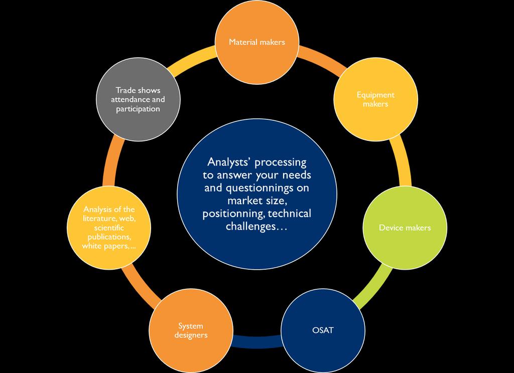

5 REPORT METHODOLOGY Technology analysis methodology Information collection 5
6 TABLE OF CONTENTS Scope Of the Report p8 Objective Of the Report p9 Who should Be Interested In this Report? p10 Companies cited in the report p11 Acronyms p12 Executive Summary p13 What is a MicroLED displays? Status Remaining Roadblocks MicroLED Attributes vs Application Requirement SWOT Analysis Major Technology Bricks Assembly Technologies Display Structure and Backplane MicroLED efficiency MicroLED Dimensions Epitaxy Chip Manufacturing Color Conversion Cost Drivers Defect Management Major Players Supply chain Possible Winner and Losers. MicroLED Application Roadmap MicroLED Adoption Forecast What s Happening In the Short Term? Introduction p52 LED Efficiency Display Resolutions OLED and LCD Display structure Overview Display Trends LEDs In displays MicroLED Definition and History MicroLED Displays Technology Evolution What is a MicroLED displays? MicroLED Display Assembly MicroLED Chip Manufacturing Benefits Comparisons With LCD and OLED MicroLED Display Manufacturing Challenges MicroLED Displays Frontplane & Pixel Structures p68 Backplane and Pixel Bank Structure MicroLED Display Structure: Monochrome MicroLED Display Structure: Color Pixel Fill Factor and Added Display Functionalities Pixel density and Pixel Pitch Subassembly Microsystems Tiled Arrays LED Efficiency Brightness Pixel Size vs. Efficiency MicroLED Driving Regime 6
7 TABLE OF CONTENTS Ultra High Brightness MicroDisplays MicroLED Large video displays Current confinement Trenches MicroLED efficiency MicroLED Dimensions MicroLED Displays Backplanes p91 Passive Matrix Driving Active Matrix Driving LCD vs Emissive display Driving Requirement Emissive Display Driving Thin Film Transistor Backplanes TFT Substrates Example: Gen 10 TFT Channel Material Trends Channel Materials For MicroLED Displays Pixel Density and Backplane Impact on MicroLED Driving Technology Impact on MicroLED Assembly Technology Discrete Micro-Controllers MicroLED Epitaxy p106 (Front End Level 0) Overview Epitaxy Defects and Dead Pixels Wavelength homogeneity and Consistency Brightness and Voltage Variations Impact on Supply chain Chip Manufacturing and Singulation p115 (front End Level 1) Chip singulation: Bonding and Etching: Apple-Luxvue Anchor and Breakable Tethers: X-Celeprint Chip Manufacturing Impact on Supply chain Transfer And Assembly Technologies p125 Pick and Place vs Monolithic Arrays Massively Parallel Pick and Place and Printing Processes p127 Overview Transfer Sequences Transfer Array Vs. Display Pixel Pitch Throughput and cost Drivers Edge Effects Pick and Place Processes Die Stabilization and Release. Die Selection Pick Up Methods Luxvue: Electrostatic MEMS Luxvue Compliant Pick Up Heads Luxvue Transfer Process Sequence Luxvue Alternative Process X-Celeprint Elastomere Transfer Printing Other Process Flows: Die Encapsulation Other Process Flows: Stretchable Film Semi-continuous Process 7
8 TABLE OF CONTENTS Wet Printing, Electrophotographic Fluidic Assembly Key IP Holders and Conclusion Large Monolithic MicroLED Arrays p160 The challenge for High Pixel Density Full Array Level Microdisplay Manufacturing. Hybridization MicroLED Array Hybridization on CMOS: LETI Monolithic Integration of LTPS TFT: Lumiode Monolithic Integration of Metal Oxide TFT: emagin Monolithic Integration of GaN TFT: OSRAM and Nth Degree Micro-wire MicroLED Arrays: Aledia 3D Integration: Ostendo Conclusion Light Extraction and Viewing Angles p175 Introduction Die-Level Beam Shaping and Extraction Illustration: InfiniLED Array-Level Beam Shaping External Micro Optics Viewing Angle and Power consumption Color Conversion p183 Color Gamut Comparison of major standards Major Color Gamut in the CIE 1931 and 1976 spaces Color Conversion Wavelength Converter Deposition Broadband phosphors Narrowband Phosphors Examples Phosphors Particle size Quantum Dots Benefits and challenges Performance Implementations in Traditional Displays Challenges for MicroLED Displays QD vs Phosphors: Summary Quantum Wells converters. Defect Management p201 Introduction Bad Pixels Emitter Redundancy Example of Repair Strategies Defect Management Strategies Conclusion Applications and Markets for MicroLED Displays p212 Overview Of Key Hypothesis Overview of Epiwafer Cost per Application Overview of Epiwafer And Transfer Cost per Application Discussion MicroLED Attributes vs Application Requirement MicroLED Application Roadmap MicroLED SWOT Per Application MicroLED Adoption Forecast 8
9 TABLE OF CONTENTS Virtual Reality p224 Introduction: VR and AR/MR The Reality-to-Virtual-Reality Continuum. VR Displays: FOV, Resolution and Pixel Density VR Displays: Refresh Rate VR Displays: Brightness Computing Power and Bandwidth Foveated rendering Trade Offs for the Design of a VR Headset Current status Microdisplays MicroLED displays for VR: Transfer-Based (Large displays) Screen Door Effect MicroLED Microdisplays MicroLED displays for VR: conclusion Augmented and Mixed Reality p244 Display Requirements Display Types: MicroLED Displays for AR and MR Comparison of AR Displays Technologies AR/MR Market Forecast MicroLED Scenario for AR/MR. Head Up displays MicroLED Head Up displays Forecast Smartwatches p253 Introduction Forecasting the Smartwatch market MicroLED for Smartwatches Forecast MOCVD Requirement Transfer Tools Requirements TVs p262 Introduction The UHD alliance MicroLED vs OLED and QD-LCD MicroLED TV Panel costs Additional Challenges For MicroLED TVs MicroLED Volume forecast and MOCVD Requirements Transfer Tools Requirements Alternative Transfer and Assembly Approaches Smart Phones p273 Smartphone display Requirement Is 4K required? MicroLED for Cell Phones: Epiwafer Cost MicroLED for Cell Phones: Transfer Cost No Pixel Redundancy Pixel Redundancy Status and roadblocks Volume forecast and MOCVD Requirements Transfer Tools Requirements Tablets p284 MicroLED Tablet Panel costs Volume forecast and MOCVD Requirements Transfer Tools Requirements 9
10 TABLE OF CONTENTS Laptops and Convertibles p289 Tablet, Laptops and convertible: Overview MicroLED in Laptops MicroLED Laptop Panel costs Volume forecast and MOCVD Requirements Transfer Tools Requirements Desktop Monitors p296 Desktop Computer Monitors Volume forecast and MOCVD Requirements Transfer Tools Requirements Large video displays p301 Overview MicroLED Large Video Displays Supply Chain p317 Overview Summary of Key Hypothesis Substrate and MOCVD Requirements Discussion: Wafer Supply Epitaxy and Wafer Processing Transfer Tools Impact on Supply chain Supply Chain Scenario Discussion Company presentation p333 Others p304 LCD Backlights Competitive Landscape p308 Research Activity Leading Patent Holders Key Players and Technology Focus Significant Industry Events The Apple Ecosystem Taiwan Ecosystem Discussion 10
11 ACRONYMS AR:Augmented Reality CapEx: Capital Expenditure CMOS: Complementary Metal Oxide Semiconductor EQE: External Quantum Efficiency FET: Field Effect Transistor FHD: Full High Definition (1920 x 1080) FOV: Field Of View FWHM: Full Width at Half Maximum HD: High Definition HMD: Head Mounted Display HUD: Head Up Display IC: Integrated Circuit IQE: Internal Quantum Efficiency LCD: Liquid Crystal Display LCOS: Liquid Crystal On Silicon LED: Light Emitting Diode MEMS: Micro Electro-Mechanical Systems MOCVD: Metal-Oxide Chemical Vapor Deposition MR: Mixed Reality ODM: Original Design Manufacturer OEE: Optical Extraction Efficiency OEM: Original Equipment Manufacturer OLED: Organic Light emitting Diode PDMS: Polydimethylsiloxane (polymer material) PECVD: Plasma-Enhanced Chemical Vapor Deposition P&P: Pick and Place PPD: Pixel Per Degree PPI: Pixel Per Inch PPM: Parts Per Million QD: Quantum Dots QHD: Quad High Definition (2560 x 1400 to 3440 x 1440) TFT:Thin Film Transi LTPS: Low Temperature Polysilicon 11
12 WHO SHOULD BE INTERESTED IN THIS REPORT LED supply chain: sapphire makers, MOCVD suppliers, epi-houses. Understand the µled display opportunity What does it entail for the LED supply? What are the technical challenges? How can my company participate in this emerging opportunity? Who should we partner with? R&D Organizations and Universities Understand the market potential of your technologies for this emerging market Identify the best candidates for collaboration and technology transfer. OEMs / ODMs What are the potential benefits of µled displays? Are they a threat or an opportunity for my products? When will they be ready Should I get involved in the supply chain. Display Makers and supply chain Hype versus reality: what is the status of µled displays? What can we expect in the near future? Are they a threat to my LCD and OLED investments? Which display applications and markets can µled displays address? A detailed roadmap. Find the right partner: detailed mapping of the µled ecosystem and supply chain OSAT and foundries Are µled a new opportunity for my company? Venture capital, financial and strategic investors. Hype versus reality. Understand the technology and the real potential. How is the supply chain shaping up? Identify the key players and potential investment targets. Could µled hurt my existing investments? 12
13 COMPANIES CITED IN THE REPORT Aledia (FR), Allos Semiconductor (DE), Apple (US), AUO (TW), BOE (CN), CEA-LETI (FR), CIOMP (CN), Columbia University (US), Cooledge (CA), Cree (US), CSOT (CN), emagin (US), Epistar (TW), Epson (JP), Facebook (US), Foxconn (TW), Fraunhofer Institute (DE), Glo (SE), GlobalFoundries (US), Goertek (CN), Hiphoton (TW), HKUST (HK), HTC (TW), Ignis (CA), InfiniLED (UK), Intel (US), ITRI (TW), Kansas State University (US), Kopin (US), Lumiode (US), Luxvue (US), Metavision (US), Microsoft (US), Mikro-Mesa (TW), mled (UK), Nichia (JP), Nth Degree (US), Oculus (US), Osterhout Design Group (US), Osram (DE), Ostendo (US), Playnitride (TW), PSI Co (KR), Rohinni (US), Saitama University (JP), Samsung (KR), Sanan (CN), Semprius (US), Sharp (JP), Sony (JP), Strathclyde University (UK), Sun Yat-Sen University (TW),Texas Tech (US),TSMC (TW), Tyndall National Institute (IE), University of Illinois (US),VerLASE (US),VueReal (CA),Vuzix (US), X-Celeprint (IE). 13

14 ABOUT THE AUTHOR Biography & contact Contact: Eric Virey is a Senior Market and Technology Analyst at Yole Développement. Eric is a daily contributor to the development of LED, OLED, and Displays activities at Yole, with a large collection of market and technology reports as well as multiple custom consulting projects: business strategy, identification of investments or acquisition targets, due diligences (buy/sell side), market and technology analysis, cost modelling, technology scouting, etc. Thanks to its deep knowledge of the LED/OLED and displays related industries, Eric has spoken in more than 30 industry conferences worldwide over the last 5 years. He has been interviewed and quoted by leading media over the world. Previously Eric has held various R&D, engineering, manufacturing and business development positions with Fortune 500 Company Saint-Gobain in France and the United States. Dr Eric Virey holds a Ph-D in Optoelectronics from the National Polytechnic Institute of GrenobleEric is also author / co-author of multiple reports (examples below) and contributed to various custom projects. LED Packaging LED Front End Manufacturing III-V Epitaxy Bulk GaN GaN on Silicon Status of the LED Industry Sapphire Market & Applications Phosphors and Quantum Dots Organic TFTs 14
15 Report sample 2017


16 LEDS IN DISPLAYS Traditional SMD or CSP packaged LEDs are commonly used as the illumination source for the backlighting of LCD panels. LEDs are also commonly used in large direct emissive video billboards used in stadium, advertising and video facades. In those devices, discrete packaged LED containing red, green and blue chips form the individual pixels with pitches typically ranging from 1 to 40 mm depending on display size and resolution. Packaged LEDs are commonly used in large video displays and LCD backlight. MicroLEDs could be at the center of a new display revolution As of Q1-2017, there is no other format of commercial displays using LEDs as a direct emissive element to constitute individual pixels or sub-pixels. The reasons for this limitation are multiple and include cost and manufacturability. Nevertheless, the idea of µled displays with high resolution and sub millimetric pixel pitch is almost as old as the invention and commercialization of LEDs themselves. Over the last 3-4 years it has generated a lot of excitement and development as well as investment and M&A activity. Packaged LED LED Video display Illustration: 16
 or out of reach? Small pitch (<2 mm) large video displays.")
 Large die OK (30 µm) but low transfer efficiency.")
17 MICROLED APPLICATION ROADMAP Now (2017) Soon) (2-3 years) Mid term (3-5 year) Longer term (>5 years) or out of reach? Small pitch (<2 mm) large video displays. Brings significant performance improvement (contrast) and potential cost reduction (eliminates LED package) Large die OK (30 µm) but low transfer efficiency. Available from Sony in 2017: Detailed roadmap in the report 17
, while other ones have acquired IPs through patent licensing agreements (XXX, XXX, XXX) or M&A")
18 LEADING PATENT HOLDERS 140+ players have filed patents related to microled.the 500+ microled inventions are held by a lot of different patent applicants. Some players have filed their own patents (XXX, XXX, XXX, XXX, XXX, XXX, XXX, XXX, XXX, XXX, XXX ), while other ones have acquired IPs through patent licensing agreements (XXX, XXX, XXX) or M&A (Apple/LuxVue, Oculus/InfiniLED). Many R&D Labs are present in the microled patent landscape (University of Illinois, ITRI, CEA-LETI, CIOMP, Fraunhofer, Sejong University ). * A patent family is a set of patents filed in multiple countries by a common inventor(s) to protect a single invention. Industrials R&D Labs 18
19 MAJOR PLAYERS Epitaxy µled structure Transfer and interconnect Hybridization Testing and repair / Defect Management Color Conversion Light Extraction & shaping Display architecture & drivers Details in the report 19
.")

20 MicroLED DISPLAY ASSEMBLY The art of making µled displays consists in processing a bulk LED substrate into an array of micro-leds which are poised for pick up and transfer to a receiving substrate for integration into heterogeneously integrated system: the display (which integrates, LEDs, transistors, optics etc ). The micro-leds can be picked up and transferred individually, in groups, or as the entire array of 100,000 s of µleds: MicroLED chips can be singulated and transferred individually or as large monolithic arrays. Massively Parallel Transfer ( Pick and Place ) Individual µled dies or small chips comprising small amounts of µled emitters (<10) are singulated and individually picked up, transferred, positioned and assembled to a backplane containing the pixel driving circuitry (typically TFT on glass or flexible substrate). The pitch on the display is typically lower than that of the donor wafer. µled chips Arrays Monolithic Integration Large chips comprising large quantities of µled emitters (>10,000 s to millions) are hybridized onto a backplane (typically Si CMOS). Individual pixels are not physically singulated. The pitch of the donor array matches the pitch of the display. µled array Backplane Epiwafer or carrier with pre-singulated die Transfer Tool Backplane Hybridization Display Backplane Epiwafer 20

21 BACKPLANE AND PIXEL BANK STRUCTURE Backplane Frontplane The TFT backplane can be essentially identical to that of an OLED display all the way through the planarization layer. The front plane structure including the interconnects and the pixel banks can be built directly upon the backplane. The bank layer thickness and angle can be used to adjust the display viewing angle. µled dies are positioned into the pixel bank by the transfer tool and connected by solder reflow or other processes. More than 1 µled of the same color can be placed in each bank if redundancy is required to mitigate risks of dead/malfunctioning pixels (see Defect Management section of this report) Drain Bank layer Electrode to pixel Passivation Channel (semiconductor) Gate Insulator Gate (metal) Gate Insulator (Dielectric) Light Source Bottom electrode Backplane substrate (Glass, metal, plastic) Cross section of a microled display subpixel Sub pixel Transparent electrode Passivation Planarization Layer (Also known as Interlayer Dielectric: ILD) Other circuitry (not detailed): switch transistors, compensation transistors, capacitors, Subpixel bank Simplified top view of the pixel bank Pixel bank 21

22 EXAMPLE OF TRANSFER SEQUENCES 1) Transfer array 3) Transfer array Transfer array Display substrate Transfer array Display substrate 2) 4) Donor wafer Display substrate Donor wafer Display substrate Transfer sequence to populate a 8x8 monochromatic display from a single donor wafer in 4 steps. 22


23 PICK AND PLACE PROCESSES Dozens of transfer technologies have been proposed. The major technology options identified by screening more than 450 are shown here Die Stabilization and release: How to provide enough force to hold the die onto the donor wafer but allow its release to the pick up heads Release Die Selection: The pitch of the µleds on the donor wafer is usually smaller than that on the display. Some die need to be picked up while others remain on the donor wafer Die Pick Up: Provide enough force to overcome the bonding force of the die to the donor wafer to allow pick up. Die Placing Provide enough force to overcome the bonding force of the die to the transfer array and drop it off on the receiving substrate Stabilization Donor wafer Donor wafer Donor wafer Display backplane 23

24 KEY IP HOLDERS AND CONCLUSION More than 20 companies have patented massively parallel transfer processes for µleds. Many more processes could be inferred by combining the different technology bricks described in this section. Main patent applicants involved in massively parallel pick and place technology (according to the number of their patent families*) Mass transfer is a cornerstone of µled display technologies. Luxvue and X- Celeprint have solid IP portfolio on the topic. Most are probably just concepts that haven t yet reached the stage of prototypes. None has yet been fully validated in volume production to the exception of the PDMS stamp process developed by the team of Prof. Rogers at the University of Illinois and used by startup Semprius for photovoltaic applications. X-Celeprint is developing and commercializing the technology for µleds and other micro-devices. Beside X-Celeprint, the most advanced company in the field of massively parallel transfer of µleds is likely to be Apple via its acquisition of Luxvue in We believe their the technology to be more complex (MEMS vs polymer stamp) but deliver higher throughputs and be capable of handling smaller size of µleds. Both companies however remains secretive about actual performance of their technology. Another issue not developed in this report is that of the transfer equipment which must ensure very high positioning accuracy at both the pick up and drop off steps. Multiple patents describing transfer tools have been filed by XXX, XXX, XXX etc. Source: * A patent family is a set of patents filed in multiple countries by a common inventor(s) to protect a single invention. 24
25 DEFECT MANAGEMENT STRATEGIES Added epi cost Added epi cost Illustrations: reducing die size to a level where redundancy becomes cost effective, i.e. when decrease in repair cost offsets epiwafer cost increase. The graph shows our simulation for various applications of the epiwafer cost thresholds and corresponding die size at which redundancy becomes cost effective For displays with high pixel counts and pixel density, pixel repair dominates the transfer cost. Pixel redundancy becomes efficient if die size can be reduced. Die size $XX Die size $XX $XX $XX Die size Die size 25
26 OVERVIEW OF EPIWAFER AND TRANSFER COST PER APPLICATION [1] Smartwatch QHD Smartphone (Galaxy S7 ) 4K Smartphone (Xperia Z5 Premium) 9 Tablet (ipad Pro) 13 Laptop (MacBook Pro) FHD Monitor 4K Monitor 4K 55" TV 8K 85" TV Resolution 312 x x x x x x x x x 4320 PPI # of transfer cycles [2] XX XX XX XX XX XX XX XX XX # of repairs at 100 ppm defects Total Transfer cost Total Epiwafer cost 37 1,106 2, , ,489 2,489 9,954 XX XX XX XX XX XX XX XX XX XX XX XX XX XX XX XX XX XX Total XX XX XX XX XX XX XX XX XX Total with redundancy [3] XX XX XX XX XX XX XX XX XX [1] cost for transfer and epiwafer only. Doesn t include: backplane, color conversion, optics, testing [2]: assumes XxX cm 2 transfer array [3]: assumes Xx subpixel redundancy: doubles epiwafer cost and the number of transfer cycles but put repair cycles at zero. 26


27 MICROLED SWOT PER APPLICATION 27


28 TRADE OFFS FOR THE DESIGN OF A VR HEADSET Sony 28

29 MOCVD REQUIREMENT Assuming displays realized with XX x XX µm size µleds, about XXx multiwafer (Veeco s Epik 700 type) or XXX single-wafer reactors would be needed to supply Apple needs. If the µled size can be reduced to XX x XX µm, the numbers drop to XX and XX respectively. Note however that those numbers assume a production run rate averaged throughout the year. Higher numbers (+20~30%) would be needed to absorb the higher run-rates typically experienced in the few the months preceding a product launch. XX x XX µm MicroLED Scenario with 2x redundancy Smartwatch market would put only moderate strain on the LED supply chain # of 6" epiwafers # of MOCVD (12 x 6") # of 8" Epiwafers # of MOCVD (1 x 8") # of 6" epiwafers # of MOCVD (12 x 6") # of 8" Epiwafers # of MOCVD (1 x 8") XX x XX µm MicroLED Scenario with 2x redundancy Note: indicates total cumulated # of MOCVD tools 29


30 RELATED REPORTS Discover more related reports within our bundles here. 30
31 ORDER FORM Please process my order for MicroLED Displays Reverse Costing Report Ref.: YDLS17003 Full Reverse Costing report: EUR 6,490* Annual Subscription (including this report as the first of the year): o 3 reports EUR 8 400* o 5 reports EUR * o 7 reports EUR * o 10 reports EUR * o 15 reports EUR * *For price in dollars please use the day s exchange rate *All reports are delivered electronically in pdf format *For French customer, add 20 % for VAT *Our prices are subject to change. Please check our new releases and price changes on The present document is valid 6 months after its publishing date: February 2017 SHIP TO Name (Mr/Ms/Dr/Pr):... Job Title:... Company:... Address:... City: State:... Postcode/Zip:... Country:... VAT ID Number for EU members:... Tel: Date:... Signature:... BILLING CONTACT First Name:... Last Name: Phone:... PAYMENT DELIVERY on receipt of payment: By credit card: Number: Expiration date: / Card Verification Value: By bank transfer: HSBC - CAE- Le Terminal -2 rue du Charron St Herblain France BIC code: CCFRFRPP In EUR Bank code : Branch code : Account : IBAN: FR In USD Bank code : Branch code : Account : IBAN: FR Return order by: FAX: MAIL: SYSTEM PLUS CONSULTING 21 rue La Nouë Bras de Fer Nantes France Contact: sales@systemplus.fr TEL: ABOUT SYSTEM PLUS CONSULTING System Plus Consulting is specialized in the cost analysis of electronics from semiconductor devices to electronic systems. A complete range of services and costing tools to provide in-depth production cost studies and to estimate the objective selling price of a product is available. Our services: TECHNOLOGY ANALYSIS - COSTING SERVICES - COSTING TOOLS - TRAININGS - sales@systemplus.fr Performed by
32 TERMS AND CONDITIONS OF SALES 1.INTRODUCTION The present terms and conditions apply to the offers, sales and deliveries of services managed by System Plus Consulting except in the case of a particular written agreement. Buyer must note that placing an order means an agreement without any restriction with these terms and conditions. 2.PRICES Prices of the purchased services are those which are in force on the date the order is placed. Prices are in Euros and worked out without taxes. Consequently, the taxes and possible added costs agreed when the order is placed will be charged on these initial prices. System Plus Consulting may change its prices whenever the company thinks it necessary. However, the company commits itself in invoicing at the prices in force on the date the order is placed. 3.REBATES and DISCOUNTS The quoted prices already include the rebates and discounts that System Plus Consulting could have granted according to the number of orders placed by the Buyer, or other specific conditions. No discount is granted in case of early payment. 4.TERMS OF PAYMENT System Plus Consulting delivered services are to be paid within 30 days end of month by bank transfer except in the case of a particular written agreement. If the payment does not reach System Plus Consulting on the deadline, the Buyer has to pay System Plus Consulting a penalty for late payment the amount of which is three times the legal interest rate. The legal interest rate is the current one on the delivery date. This penalty is worked out on the unpaid invoice amount, starting from the invoice deadline. This penalty is sent without previous notice. When payment terms are over 30 days end of month, the Buyer has to pay a deposit which amount is 10% of the total invoice amount when placing his order. 5. OWNERSHIP System Plus Consulting remains sole owner of the delivered services until total payment of the invoice. 6.DELIVERIES The delivery schedule on the purchase order is given for information only and cannot be strictly guaranteed. Consequently any reasonable delay in the delivery of services will not allow the buyer to claim for damages or to cancel the order. 7.ENTRUSTED GOODS SHIPMENT The transport costs and risks are fully born by the Buyer. Should the customer wish to ensure the goods against lost or damage on the base of their real value, he must imperatively point it out to System Plus Consulting when the shipment takes place. Without any specific requirement, insurance terms for the return of goods will be the carrier current ones (reimbursement based on good weight instead of the real value). 8.FORCE MAJEURE System Plus Consulting responsibility will not be involved in non execution or late delivery of one of its duties described in the current terms and conditions if these are the result of a force majeure case. Therefore, the force majeure includes all external event unpredictable and irresistible as defined by the article 1148 of the French Code Civil? 9.CONFIDENTIALITY As a rule, all information handed by customers to system Plus Consulting are considered as strictly confidential. A non-disclosure agreement can be signed on demand. 10.RESPONSABILITY LIMITATION The Buyer is responsible for the use and interpretations he makes of the reports delivered by System Plus Consulting. Consequently, System Plus Consulting responsibility can in no case be called into question for any direct or indirect damage, financial or otherwise, that may result from the use of the results of our analysis or results obtained using one of our costing tools. 11.APPLICABLE LAW Any dispute that may arise about the interpretation or execution of the current terms and conditions shall be resolved applying the French law. It the dispute cannot be settled out-of-court, the competent Court will be the Tribunal de Commerce de Nantes. Performed by
33 Yole Développement From Technologies to Market 2017


34 FIELDS OF EXPERTISE Yole Développement s 30 analysts operate in the following areas Photonics Imaging MEMS & Sensors RF Devices & Techno. Displays MedTech LED Manufacturing Compound Semi. Advanced Packaging Power Electronics Batteries / Energy Management Advanced Substrates 32
35 4 BUSINESS MODELS o Consulting and Analysis Market data & research, marketing analysis Technology analysis Strategy consulting Reverse engineering & costing Patent analysis o Financial services M&A (buying and selling) Due diligence Fundraising Maturation of companies IP portfolio management & optimization o Reports o Market & technology reports Patent Investigation and patent infringement risk analysis Teardowns & reverse costing analysis Cost simulation tool Media i-micronews.com e-newsletter Communication & webcast services Events 33


36 A GROUP OF COMPANIES M&A operations Due diligences Innovation and business maker Market, technology and strategy consulting Manufacturing costs analysis Teardown and reverse engineering Cost simulation tools IP analysis Patent assessment Test & Measurement Expertise Research & Innovation 34
37 OUR 2017 REPORTS PLANNING (1/2) MARKET AND TECHNOLOGY REPORTS by Yole Développement o MEMS & SENSORS Fingerprint Sensor Applications and Technologies - Consumer Market Focus 2017 MEMS Microphones, Speakers and Audio Solutions 2017 Status of the MEMS Industry 2017 MEMS & Sensors for Automotive 2017 High End Inertial Sensors for Defense and Industrial Applications 2017 Sensor Modules for Smart Building 2017 Sensing and Display for AR/VR/MR 2017 (Vol 1) MEMS Packaging 2017 Magnetic Sensors Market and Technologies 2017** Microspectrometers Markets and Applications 2017** o RF DEVICES AND TECHNOLOGIES RF Components and Modules for Cellphones 2017 Advanced RF SiP for Cellphones G and Beyond (Vol 1): Impact on RF Industry, from Infrastructure to Terminals G and Beyond (Vol 2): RF Materials Platform, from Infrastructure to Terminals 2017 RF Technologies for Automotive Applications 2017 GaN and Si LDMOS Market and Technology Trends for RF Power 2017 o IMAGING & OPTOELECTRONICS 3D Imaging & Sensing 2017 Status of the CMOS Image Sensor Industry 2017 Camera Module for Consumer and Automotive Applications 2017 Uncooled Infrared Imaging Technology & Market Trends 2017 Active Imaging and Lidars 2017 (vol 1) o MEDTECH Status of the Microfluidics Industry 2017 Solid State Medical Imaging 2017 Sensors for HomeCare 2017 Sensors for Medical Robotics 2017 Organs-on-a Chip 2017 o ADVANCED PACKAGING Advanced Substrates Overview 2017 Status of the Advanced Packaging Industry 2017 Fan Out Packaging: Market & Technology Trends D Business Update: Market & Technology Trends 2017 Advanced QFN: Market & Technology Trends 2017** Inspection and Metrology for Advanced Packaging Platform 2017** Advanced Packaging for Memories 2017 Embedded Die Packaging: Technologies and Markets Trends 2017 o MANUFACTURING Glass Substrate Manufacturing 2017 Equipment & Materials for Fan Out Technology 2017 Equipment & Materials for 3D T(X)V Technology 2017 Emerging Non Volatile Memories 2017 ** To be confirmed 35
38 OUR 2017 REPORTS PLANNING (2/2) o POWER ELECTRONICS Status of Power Electronics Industry 2017 Power Mosfets Market and Technology Trends 2017 IGBT Market and Technology Trends 2017 Power Packaging Market and Technology Trends 2017 Power SiC 2017: Materials, Devices, and Applications Power GaN 2017: Materials, Devices, and Applications Materials Market Opportunities for Cellphone Thermal Management (Battery Cooling, Fast Charging, Data Processing, Battery Cooling, etc.) 2017 Gate Driver Market and Technology Trends in Power Electronics 2017 Power Management ICs Market Quarterly Update 2017 Power Electronics for Electrical Aircraft, Rail and Buses 2017 Thermal Management for LED and Power 2017 o BATTERY AND ENERGY MANAGEMENT Status of Battery Industry for Stationary, Automotive and Consumer Applications 2017 o o COMPOUND SEMICONDUCTORS Power SiC 2017: Materials, Devices, and Applications Power GaN 2017: Materials, Devices, and Applications GaN and Si LDMOS Market and Technology Trends for RF Power 2017 Bulk GaN Technology Status and Market Expectations (Power, LED, Lasers) 2017 DISPLAYS Microdisplays and MicroLEDs 2017 Display for Augmented Reality, Virtual Reality and Mixed Reality 2017 QD for Display Applications 2017 Phosphors & Quantum Dots LED Downconverters for Lighting & Displays Emerging Display Technologies 2017** o LED UV LEDs Technology, Manufacturing and Application Trends Agricultural Lighting Technology, Industry and Market Trends Automotive Lighting Technology, Industry and Market Trends Active Imaging and Lidar 2017 (Vol 2) - IR Lighting** LED Lighting Module Technology, Industry and Market Trends IR LEDs Technology, Manufacturing and Application Trends Phosphors & Quantum Dots LED Downconverters for Lighting & Displays CSP LED Module 2017 LED Packaging 2017 PATENT ANALYSIS by Knowmade 3D Monolithic Memory: Patent Landscape Analysis Microfluidic Diagnostic: Patent Landscape Analysis GaN Technology: Top-100 IP profiles** Uncooled Infrared Imaging: Patent Landscape Analysis** MEMS Microphone: Patent Landscape Analysis** MEMS Microphone: Knowles' Patent Portfolio Analysis** MicroLEDs: Patent Landscape Analysis** Microbolometer: Patents used in products** Micropumps: Patent Landscape Analysis** Flexible batteries: Patent Landscape Analysis** TEARDOWN & REVERSE COSTING by System Plus Consulting More than 60 teardowns and reverse costing analysis and cost simulation tools to be published in ** To be confirmed 36
39 OUR 2016 PUBLISHED REPORTS LIST MARKET AND TECHNOLOGY REPORTS by Yole Développement o MEMS & SENSORS Gas Sensors Technology and Market 2016 Status of the MEMs Industry 2016 Sensors for Cellphones and Tablets 2016 Market and Technology Trends of Inkjet Printheads 2016 Sensors for Biometry and Recognition 2016 Silicon Photonics 2016 o IMAGING & OPTOELECTRONICS Status of the CMOS Image Sensor Industry 2016 Uncooled Infrared Imaging Technology & Market Trends 2016 Imaging Technologies for Automotive 2016 Sensors for Drones & Robots: Market Opportunities and Technology Evolution 2016 o MEDTECH BioMEMS 2016 Point of Care Testing 2016: Application of Microfluidic Technologies o ADVANCED PACKAGING Embedded Die Packaging: Technology and Market Trends D & 3D IC TSV Interconnect for Advanced Packaging: Business Update 2016 Fan-Out: Technologies and Market Trends 2016 Fan-In Packaging: Business update 2016 Status and Prospects for the Advanced Packaging Industry in China 2016 o MANUFACTURING Thin Wafer Processing and Dicing Equipment Market 2016 Emerging Non Volatile Memories 2016 o COMPOUND SEMICONDUCTORS Power GaN 2016: Epitaxy and Devices, Applications and Technology Trends GaN RF Devices Market: Applications, Players, Technology and substrates 2016 Sapphire Applications & Market 2016: from LED to Consumer Electronics Power SiC 2016: Materials, Devices, Modules, and Applications o LED UV LED Technology, Manufacturing and Applications Trends 2016 OLED for Lighting 2016 Technology, Industry and Market Trends Automotive Lighting: Technology, Industry and Market Trends 2016 Thermal Management Technology and Market Perspectives in Power Electronics and LEDs 2017 Organic Thin Film Transistor 2016: Flexible Displays and Other Applications Sapphire Applications & Market 2016: from LED to Consumer Electronics LED Packaging 2017: Market, Technology and Industry Landscape o POWER ELECTRONICS Power Electronics for EV/HEV 2016: Market, Innovations and Trends Status of Power Electronics Industry 2016 Passive Components Technologies and Market Trends for Power Electronics 2016 Power SiC 2016: Materials, Devices, Modules, and Applications Power GaN 2016: Epitaxy and Devices, Applications, and Technology Trends Inverter Technologies Trends & Market Expectations 2016 Opportunities for Power Electronics in Renewable Electricity Generation 2016 Thermal Management Technology and Market Perspectives in Power Electronics and LEDs 2017 GaN RF Devices Market: Applications, Players, Technology and substrates 2016 o BATTERY AND ENERGY MANAGEMENT Beyond Li-ion Batteries: Present and Future Li-ion Technology Challengers 2016 Stationary Storage and Automotive Li-ion Battery Packs 2016 Opportunities for Power Electronics in Renewable Electricity Generation

40 CONTACT INFORMATION o CONSULTING AND SPECIFIC ANALYSIS North America: Steve LaFerriere, Director of Northern America Business Development laferriere@yole.fr Japan & Rest of Asia: Takashi Onozawa, General Manager, Asia Business Development onozawa@yole.fr Greater China: Mavis Wang, Director of Greater China Business Development wang@yole.fr RoW: Jean-Christophe Eloy, CEO & President, Yole Développement eloy@yole.fr o REPORT BUSINESS North America: Steve LaFerriere, Director of Northern America Business Development laferriere@yole.fr Europe: Lizzie Levenez, EMEA Business Development Manager levenez@yole.fr Rest of Asia: Takashi Onozawa, General Manager, Asia Business Development onozawa@yole.fr Japan & Asia: Miho Othake, Account Manager ohtake@yole.fr Greater China: Mavis Wang, Director of Greater China Business Development wang@yole.fr Follow us on o o FINANCIAL SERVICES Jean-Christophe Eloy, CEO & President eloy@yole.fr GENERAL info@yole.fr
MicroLED Displays: Global Trends & Opportunities for Equipment and Material Suppliers
 Picture: Sony From Technologies to Market MicroLED Displays: Global Trends & Opportunities for Equipment and Material Suppliers SEMICON EUROPA Jean-Christophe ELOY - CEO - Yole Développement 2017 AGENDA
STMicroelectronics Proximity Sensor & Flood Illuminator Time of Flight & Illumination device from Apple iphone X
 STMicroelectronics Proximity Sensor & Flood Illuminator Time of Flight & Illumination device from Apple iphone X IMAGING report by Stéphane ELISABETH January 2018 version 1 21 rue la Noue Bras de Fer 44200
MicroLED Displays: Hype and reality, hopes and challenges
 From Technologies to Market MicroLED Displays: Hype and reality, hopes and challenges Picture: Sony Sample 2017 SCOPE OF THE REPORT Large video displays Smartwatches and wearables Sony TV The report provides
Qualcomm VIVE QCA9500 First WiGig Chipset in 60 GHz Band
 Qualcomm VIVE QCA9500 First WiGig Chipset in 60 GHz Band RF report by Stéphane ELISABETH January 2018 21 rue la Noue Bras de Fer 44200 NANTES - FRANCE +33 2 40 18 09 16 info@systemplus.fr www.systemplus.fr
2-Axis Gyroscopes for Optical Image Stabilization: STMicroelectronics L2G2IS and InvenSense IDG-2030
 2-Axis Gyroscopes for Optical Image Stabilization: STMicroelectronics L2G2IS and InvenSense IDG-2030 Complete reports and comparison of the latest generation products for smartphones from the leading optical
Title: STMicroelectronics NIR Camera Sensor Pages: 97 Date: December 2017 Format: PDF & Excel file Price: Full report: EUR 3,490
 STMicroelectronics Near Infrared Camera Sensor in the Apple iphone X The first NIR camera sensor with multiple innovations based on imager-silicon-oninsulator substrate from SOITEC, supplied and produced
Structure, Process & Cost Analysis
 Reverse Costing Structure, Process & Cost Analysis Heimann Sensor 32 x 32-array thermopile LWIR image sensor with silicon lens A small, easy to use, low-power, cheap non-contact temperature measurement
The future of microled displays using nextgeneration
 The future of microled displays using nextgeneration technologies Introduction MicroLEDs (micro-light-emitting diodes) are an emerging display technology that, as the name implies, use very small LEDs
MicroLED Displays 2018
 From Technologies to Market MicroLED Displays 2018 Courtesy of Sony Sample 2018 2017 OBJECTIVE OF THE REPORT Everything You Always Wanted to Know About µled Displays! Understand the Current Status of the
Vesper VM1000 Piezoelectric MEMS Microphone
 Vesper VM1000 Piezoelectric MEMS Microphone MEMS report by Sylvain Hallereau February 2017 21 rue la Noue Bras de Fer 44200 NANTES - FRANCE +33 2 40 18 09 16 info@systemplus.fr www.systemplus.fr 2017 System
STMicroelectronics L2G2IS 2-Axis Gyroscope for OIS
 STMicroelectronics L2G2IS 2-Axis Gyroscope for OIS MEMS report by Romain Fraux October 2016 21 rue la Noue Bras de Fer 44200 NANTES - FRANCE +33 2 40 18 09 16 info@systemplus.fr www.systemplus.fr 2016
Mass Transfer Technology A Key For Micro-LED Cinemas Commercialization
 Mass Transfer Technology A Key For Micro-LED Cinemas Commercialization Boris Kobrin, Ph.D. Sr. Associate Analyst 2018 QLED & Advanced Display Summit at Hollywood, June 27-28, 2018 Micro-LED Presentation
SEMI Flat-Panel Display Division Phosphor Technology Center of Excellence TABLE 10 MAJOR ACTIVITIES OF PTCOE Ferroelectric Liquid
 INTRODUCTION... XVIII STUDY GOALS AND OBJECTIVES... XVIII REASONS FOR DOING THIS STUDY... XVIII CONTRIBUTIONS TO THE STUDY AND FOR WHOM... XVIII SCOPE AND FORMAT... XIX METHODOLOGY... XIX INFORMATION SOURCES...
Flexible Electronics Production Deployment on FPD Standards: Plastic Displays & Integrated Circuits. Stanislav Loboda R&D engineer
 Flexible Electronics Production Deployment on FPD Standards: Plastic Displays & Integrated Circuits Stanislav Loboda R&D engineer The world-first small-volume contract manufacturing for plastic TFT-arrays
Forward-Looking Statements
 Forward-Looking Statements Information in this presentation regarding MagnaChip s forecasts, business outlook, expectations and beliefs are forward-looking statements within the meaning of the Private
TipatOr. Liquid metal switch (LMS) display technology. Avi Fogel
 display technology. Avi Fogel") TipatOr Liquid metal switch (LMS) display technology Avi Fogel 972-52-5702938 avifog@gmail.com Who is behind TipatOr TipatOr emerged from a merger of 2 expert groups in the fields of MEMS and Displays
TipatOr Liquid metal switch (LMS) display technology Avi Fogel 972-52-5702938 avifog@gmail.com Who is behind TipatOr TipatOr emerged from a merger of 2 expert groups in the fields of MEMS and Displays
ORGANIC LIGHT EMITTING DIODES (OLEDS): TECHNOLOGIES AND GLOBAL MARKETS
: TECHNOLOGIES AND GLOBAL MARKETS") ORGANIC LIGHT EMITTING DIODES (OLEDS): TECHNOLOGIES AND GLOBAL MARKETS SMC069D September 2015 Gupta A. S. Project Analyst ISBN: 1-62296-133-1 BCC Research 49 Walnut Park, Building 2 Wellesley, MA 02481
ORGANIC LIGHT EMITTING DIODES (OLEDS): TECHNOLOGIES AND GLOBAL MARKETS SMC069D September 2015 Gupta A. S. Project Analyst ISBN: 1-62296-133-1 BCC Research 49 Walnut Park, Building 2 Wellesley, MA 02481
Forward-Looking Statements
 Forward-Looking Statements Information in this presentation regarding MagnaChip s forecasts, business outlook, expectations and beliefs are forward-looking statements within the meaning of the Private
21 rue La Noue Bras de Fer Nantes - France Phone : +33 (0) website :
 website :") 21 rue La Noue Bras de Fer - 44200 Nantes - France Phone : +33 (0) 240 180 916 - email : info@systemplus.fr - website : www.systemplus.fr 2012 September - Version 1 Written by: Maher Sahmimi DISCLAIMER
21 rue La Noue Bras de Fer - 44200 Nantes - France Phone : +33 (0) 240 180 916 - email : info@systemplus.fr - website : www.systemplus.fr 2012 September - Version 1 Written by: Maher Sahmimi DISCLAIMER
1. Publishable summary
 1. Publishable summary 1.1. Project objectives. The target of the project is to develop a highly reliable high brightness conformable low cost scalable display for demanding applications such as their
Broadcom AFEM-8072 Mid&High Band Front End module in iphone 8/X
 Broadcom AFEM-8072 Mid&High Band Front End module in iphone 8/X RF report by Stéphane ELISABETH February 2018 version 1 21 rue la Noue Bras de Fer 44200 NANTES - FRANCE +33 2 40 18 09 16 info@systemplus.fr
projectors, head mounted displays in virtual or augmented reality use, electronic viewfinders
 Beatrice Beyer Figure 1. (OLED) microdisplay with a screen diagonal of 16 mm. Figure 2. CMOS cross section with OLED on top. Usually as small as fingernails, but of very high resolution Optical system
AIXTRON in EXCILIGHT project
 AIXTRON SE AIXTRON in EXCILIGHT project Gintautas Simkus ABOUT AIXTRON 2 Who we are Headquarter based in Herzogenrath, Germany Worldwide presence with 14 sales/representatives offices and production facilities
Overview of All Pixel Circuits for Active Matrix Organic Light Emitting Diode (AMOLED)
") Chapter 2 Overview of All Pixel Circuits for Active Matrix Organic Light Emitting Diode (AMOLED) ---------------------------------------------------------------------------------------------------------------
Chapter 2 Overview of All Pixel Circuits for Active Matrix Organic Light Emitting Diode (AMOLED) ---------------------------------------------------------------------------------------------------------------
MARKET OUTPERFORMERS CELERITAS INVESTMENTS
 MARKET OUTPERFORMERS CELERITAS INVESTMENTS Universal Displays (OLED) Rating: Strong Buy Stock Price: $101/share Price Target: $130/share MOP Idea of the Month: Universal Displays Business Overview: Universal
AMOLED compensation circuit patent analysis
 IHS Electronics & Media Key Patent Report AMOLED compensation circuit patent analysis AMOLED pixel driving circuit with threshold voltage and IR-drop compensation July 2013 ihs.com Ian Lim, Senior Analyst,
OLED Status quo and our position
 OLED Status quo and our position Information Day 2013 A Deep Dive into the LC&OLED Business Dr. Udo Heider Vice President OLED Darmstadt, Germany June 26, 2013 Disclaimer Remarks All comparative figures
FLEX2017 June, Monterey, USA Dr Mike Cowin, CMO, SmartKem.
 FLEX2017 June, Monterey, USA Dr Mike Cowin, CMO, SmartKem. FLEX2017 June, Monterey, USA Dr Mike Cowin, CMO, SmartKem. EU H2020 FLEXTRANs Grant Objectives A 24 month project (started September 2016) (Grant
Applied Materials. 200mm Tools & Process Capabilities For Next Generation MEMS. Dr Michel (Mike) Rosa
 Rosa") Applied Materials 200mm Tools & Process Capabilities For Next Generation MEMS Dr Michel (Mike) Rosa 200mm MEMS Global Product / Marketing Manager, Components and Systems Group (CSG), Applied Global Services
Applied Materials 200mm Tools & Process Capabilities For Next Generation MEMS Dr Michel (Mike) Rosa 200mm MEMS Global Product / Marketing Manager, Components and Systems Group (CSG), Applied Global Services
Company Overview. September MICROVISION, INC. ALL RIGHTS RESERVED.
 Company Overview September 2018 1 SAFE HARBOR STATEMENT The statements and graphics in this presentation that are not historical facts, including statements regarding our future business strategy, future
EnabLED Licensing Program for LED Luminaires and Retrofit Bulbs
 EnabLED Licensing Program for LED Luminaires and Retrofit Bulbs Philips Lighting Intellectual Property 20170313 1 Agenda Introduction Program outline Contact info Core Technology Examples This presentation
PUBLISHABLE Summary To provide OLED stacks with improved reliability Provide improved thin film encapsulation
 PUBLISHABLE Summary SCOOP is a European funded project (FP7 project number 287595 SCOOP). It is focused on OLED technology, microdisplays based on the combination of OLED with CMOS technology, and innovative
Global OLED TV Market
 Global OLED TV Market 2015-2019 Global OLED TV Market 2015-2019 Sector Publishing Intelligence Limited (SPi) has been marketing business and market research reports from selected publishers for over five
 Page 1 of 8 Main > Electronics > Computers How OLEDs Work by Craig Freudenrich, Ph.D. Introduction to How OLEDs Work Imagine having a high-definition TV that is 80 inches wide and less than a quarter-inch
9 rue Alfred Kastler - BP Nantes Cedex 3 - France Phone : +33 (0) website :
 website :") 9 rue Alfred Kastler - BP 10748-44307 Nantes Cedex 3 - France Phone : +33 (0) 240 180 916 - email : info@systemplus.fr - website : www.systemplus.fr January 2012 Written by: Maher SAHMIMI DISCLAIMER :
9 rue Alfred Kastler - BP 10748-44307 Nantes Cedex 3 - France Phone : +33 (0) 240 180 916 - email : info@systemplus.fr - website : www.systemplus.fr January 2012 Written by: Maher SAHMIMI DISCLAIMER :
Advanced Display Manufacturing Technology
 Advanced Display Manufacturing Technology John Busch Vice President, New Business Development Display and Flexible Technology Group September 28, 2017 Safe Harbor This presentation contains forward-looking
9 rue Alfred Kastler - BP Nantes Cedex 3 - France Phone : +33 (0) website :
 website :") 9 rue Alfred Kastler - BP 10748-44307 Nantes Cedex 3 - France Phone : +33 (0) 240 180 916 - email : info@systemplus.fr - website : www.systemplus.fr January 2011 - Version 1 Written by: Sylvain HALLEREAU
9 rue Alfred Kastler - BP 10748-44307 Nantes Cedex 3 - France Phone : +33 (0) 240 180 916 - email : info@systemplus.fr - website : www.systemplus.fr January 2011 - Version 1 Written by: Sylvain HALLEREAU
PICOPROJECTORS: TECHNOLOGIES AND GLOBAL MARKETS. SMC090A October Paul W. Bragulla Project Analyst ISBN:
 PICOPROJECTORS: TECHNOLOGIES AND GLOBAL MARKETS SMC090A October 2013 Paul W. Bragulla Project Analyst ISBN: 1-56965-587-1 BCC Research 49 Walnut Park, Building 2 Wellesley, MA 02481 866-285-7215, 781-489-7301
Joint Development of Ultra-Bright, Inorganic EL Light-Emitting Materials. November 2, 2005 KURARAY CO., LTD.
 Joint Development of Ultra-Bright, Inorganic EL Light-Emitting Materials November 2, 2005 KURARAY CO., LTD. Sales Trends of Display-related Products (Kuraray (standalone)) FY1994 FY1999 FY2004 Sales Ratio
FIRST CALL FOR PAPERS SID Society for Information Display INTERNATIONAL SYMPOSIUM, SEMINAR & EXHIBITION. May 19 24, 2013
 FIRST CALL FOR PAPERS SID 2013 Society for Information Display INTERNATIONAL SYMPOSIUM, SEMINAR & EXHIBITION May 19 24, 2013 VANCOUVER CONVENTION CENTER VANCOUVER, BRITISH COLUMBIA, CANADA SID SOCIETY
STMicroelectronics SiC Module Tesla Model 3 Inverter
 REVERSE COSTING STRUCTURAL, PROCESS & COST REPORT STMicroelectronics SiC Module Tesla Model 3 Inverter Power Semiconductor report by Elena Barbarini June 2018 version 1 22 Bd Benoni Goullin 44200 NANTES
MagnaChip HV7161SP 1.3 Megapixel CMOS Image Sensor Process Review
 September 21, 2005 MagnaChip HV7161SP 1.3 Megapixel Process Review For questions, comments, or more information about this report, or for any additional technical needs concerning semiconductor technology,
Technology White Paper Plasma Displays. NEC Technologies Visual Systems Division
 Technology White Paper Plasma Displays NEC Technologies Visual Systems Division May 1998 1 What is a Color Plasma Display Panel? The term Plasma refers to a flat panel display technology that utilizes
Wafer Thinning and Thru-Silicon Vias
 Wafer Thinning and Thru-Silicon Vias The Path to Wafer Level Packaging jreche@trusi.com Summary A new dry etching technology Atmospheric Downstream Plasma (ADP) Etch Applications to Packaging Wafer Thinning
Advances in Roll-to-Roll Imprint Lithography for Display Applications Using Self Aligned Imprint Lithography. John G Maltabes HP Labs
 Advances in Roll-to-Roll Imprint Lithography for Display Applications Using Self Aligned Imprint Lithography John G Maltabes HP Labs Outline Introduction Roll to Roll Challenges and Benefits HP Labs Roll
Alien Technology Corporation White Paper. Fluidic Self Assembly. October 1999
 Alien Technology Corporation White Paper Fluidic Self Assembly October 1999 Alien Technology Corp Page 1 Why FSA? Alien Technology Corp. was formed to commercialize a proprietary technology process, protected
Organic light emitting diode (OLED) displays
 displays") Ultra-Short Pulse Lasers Enable Precision Flexible OLED Cutting FLORENT THIBAULT, PRODUCT LINE MANAGER, HATIM HALOUI, APPLICATION MANAGER, JORIS VAN NUNEN, PRODUCT MARKETING MANAGER, INDUSTRIAL PICOSECOND
Ultra-Short Pulse Lasers Enable Precision Flexible OLED Cutting FLORENT THIBAULT, PRODUCT LINE MANAGER, HATIM HALOUI, APPLICATION MANAGER, JORIS VAN NUNEN, PRODUCT MARKETING MANAGER, INDUSTRIAL PICOSECOND
ADDING AN O TO LEDS STATUS AND PERSPECTIVES OF ORGANIC LIGHT EMITTING DIODES PAWEL E. MALINOWSKI, TUNGHUEI KE LED EVENT 2017
 ADDING AN O TO LEDS STATUS AND PERSPECTIVES OF ORGANIC LIGHT EMITTING DIODES PAWEL E. MALINOWSKI, TUNGHUEI KE LIVING ROOM NOT SO LONG AGO... 2 Source: Warner Bros. Incadescent CRT 3 Source: Warner Bros.
InvenSense Fabless Model for the MEMS Industry
 InvenSense Fabless Model for the MEMS Industry HKSTP Symposium Aug 2016 InvenSense, Inc. Proprietary Outline MEMS Market InvenSense CMOS-MEMS Integration InvenSense Shuttle Program and Process MEMS MARKET
Next Generation of Poly-Si TFT Technology: Material Improvements and Novel Device Architectures for System-On-Panel (SOP)
") Next Generation of Poly-Si TFT Technology: Material Improvements and Novel Device Architectures for System-On-Panel (SOP) Tolis Voutsas* Paul Schuele* Bert Crowder* Pooran Joshi* Robert Sposili* Hidayat
Next Generation of Poly-Si TFT Technology: Material Improvements and Novel Device Architectures for System-On-Panel (SOP) Tolis Voutsas* Paul Schuele* Bert Crowder* Pooran Joshi* Robert Sposili* Hidayat
The Company. A leading OLED player
 The Company A leading OLED player Novaled is the company to trade with, work for and invest in. Our company focuses on proprietary organic materials and complementary innovative technologies for superior
Picoprojectors & Light Engine 2008
 Picoprojectors & Light Engine 2008 2008 Content Executive summary Light engines Definition The applications Overview of the technologies Microdisplays Lighting Packaging Description of the different lighting
Scalable self-aligned active matrix IGZO TFT backplane technology and its use in flexible semi-transparent image sensors. Albert van Breemen
 Scalable self-aligned active matrix IGZO TFT backplane technology and its use in flexible semi-transparent image sensors Albert van Breemen Image sensors today 1 Dominated by silicon based technology on
MEMS4Display MEMS-based microdisplays market analysis. Report name : MEMS4Display Publication date : March 2006
 MEMS4Display MEMS-based microdisplays market analysis 2006 Report name : MEMS4Display Publication date : March 2006 Content Definitions and methodology The MEMS market The 2005-2010 MEMS market forecast
2016, Amkor Technology, Inc.
 1 Standardization of Packaging for the Internet of Things Adrian Arcedera l VP of MEMS and Sensor Products 2 About Amkor Technology Amkor Technology, Inc. is one of the world's largest and most accomplished
Challenges in the design of a RGB LED display for indoor applications
 Synthetic Metals 122 (2001) 215±219 Challenges in the design of a RGB LED display for indoor applications Francis Nguyen * Osram Opto Semiconductors, In neon Technologies Corporation, 19000, Homestead
Taking Technology to the Marketplace. Aram Mooradian Founder & CTO Sunnyvale, CA, USA
 Taking Technology to the Marketplace Aram Mooradian Founder & CTO Sunnyvale, CA, USA aram@novalux.com Requirements Market Technology Product Price Timing Good Investors Good People Path to Success Absolutely
VARIOUS DISPLAY TECHNOLOGIESS
 VARIOUS DISPLAY TECHNOLOGIESS Mr. Virat C. Gandhi 1 1 Computer Department, C. U. Shah Technical Institute of Diploma Studies Abstract A lot has been invented from the past till now in regards with the
Organic light emitting diodes for display technology
 Organic light emitting diodes for display technology Shamna Shamsudeen MScTI - ZITI-Heidelberg University OLED ZITI, Uni Heidelberg Page1 What s Light Light: Visible part of EM spectra. Ref:[1] Thermoluminescence:
the Most Popular Display Technology?
 Why is LCD the Most Popular Display Technology? History of Liquid Crystal Display (LCD) As early as 1889, scientists discovered that chemicals such as cholesteryl benzoate, when melted into liquid form,
LΞD2Light. December 2005
 2005 LΞD2Light December 2005 Contents Introduction HB-LED general data Global HB-LED market analysis Nitride-based LEDs market analysis White/blue GaN LED Performance and price roadmap 2 substrates volumes
Monolithic Optoelectronic Integration of High- Voltage Power FETs and LEDs
 Monolithic Optoelectronic Integration of High- Voltage Power FETs and LEDs, Zhongda Li, Robert Karlicek and T. Paul Chow Smart Lighting Engineering Research Center Rensselaer Polytechnic Institute, Troy,
Optical Engine Reference Design for DLP3010 Digital Micromirror Device
 Application Report Optical Engine Reference Design for DLP3010 Digital Micromirror Device Zhongyan Sheng ABSTRACT This application note provides a reference design for an optical engine. The design features
Bringing Better Pixels to UHD with Quantum Dots
 Bringing Better Pixels to UHD with Quantum Dots Charlie Hotz, Jason Hartlove, Jian Chen, ShihaiKan, Ernie Lee, Steve Gensler Nanosys Inc., Milpitas, CA About Nanosys World s leading supplier of Quantum
PLASMA DISPLAY PANEL (PDP) DAEWOO D I G I T A L DIGITAL TV DEVISION
 DAEWOO D I G I T A L DIGITAL TV DEVISION") PLASMA DISPLAY PANEL (PDP) DAEWOO D I G I T A L 2002. 5 DAEWOO ELECTRONICS CO., LTD DIGITAL TV DEVISION WHAT IS PLASMA DISPLAY PANEL? 1. PDP refers to plasma display panel. It was named as PDP by the faculty
PLASMA DISPLAY PANEL (PDP) DAEWOO D I G I T A L 2002. 5 DAEWOO ELECTRONICS CO., LTD DIGITAL TV DEVISION WHAT IS PLASMA DISPLAY PANEL? 1. PDP refers to plasma display panel. It was named as PDP by the faculty
2016, Amkor Technology, Inc.
 1 Standardization of Packaging for the Internet of Things Adrian Arcedera l VP of MEMS and Sensor Products 2 About Amkor Technology Amkor Technology, Inc. is one of the world's largest and most accomplished
OLED Lighting in Automotive Applications State of the Art and Future Demands. OLEDs World Summit 2017, San Francisco, Dr. Werner Thomas, AUDI AG
 OLED Lighting in Automotive Applications State of the Art and Future Demands OLEDs World Summit 2017, San Francisco, Dr. Werner Thomas, AUDI AG 2 Agenda 1. Overview 1 st automotive series applications
SEMICONDUCTOR TECHNOLOGY -CMOS-
 SEMICONDUCTOR TECHNOLOGY -CMOS- Fire Tom Wada What is semiconductor and LSIs Huge number of transistors can be integrated in a small Si chip. The size of the chip is roughly the size of nails. Currently,
DARPATech 99 DARPA/MTO. Bruce Gnade
 DARPATech 99 DARPA/MTO Bruce Gnade High Definition Systems Objective: Develop leading-edge display technology to meet diverse, but specific, DoD needs. The goals include increased power efficiency, reduced
Design of Active Matrix Micro-LED Display with CCCS Pixel Circuits
 Design of Active Matrix Micro-LED Display with CCCS Pixel Circuits Ke ZHANG 1, 2, Zhaojun LIU* 1, 2 and Hoi-Sing KWOK* 1 1 State Key Laboratory on Advanced Displays and Optoelectronics Technologies, The
PROCESS TECHNOLOGIES FOR ADVANCED ORGANIC ELECTRONIC DEVICES: MICRODISPLAYS, LIGHTING AND SOLAR CELLS
 PROCESS TECHNOLOGIES FOR ADVANCED ORGANIC ELECTRONIC DEVICES: MICRODISPLAYS, LIGHTING AND SOLAR CELLS Dr. Christian May Fraunhofer IPMS - Center for Organic Materials and Electronic Devices Dresden COMEDD
Display Technologies CMSC 435. Slides based on Dr. Luebke s slides
 Display Technologies CMSC 435 Slides based on Dr. Luebke s slides Recap: Transforms Basic 2D Transforms: Scaling, Shearing, Rotation, Reflection, Composition of 2D Transforms Basic 3D Transforms: Rotation,
Gary Mandle Sr. Product Manager Professional Display Products
 Gary Mandle Sr. Product Manager Professional Display Products rganic Light Emitting Diode It is: An emissive output o backlight o plasma gasses Self luminous matrix array Created by sandwiching several
SEMICONDUCTOR TECHNOLOGY -CMOS-
 SEMICONDUCTOR TECHNOLOGY -CMOS- Fire Tom Wada 2011/12/19 1 What is semiconductor and LSIs Huge number of transistors can be integrated in a small Si chip. The size of the chip is roughly the size of nails.
Sep 09, APPLICATION NOTE 1193 Electronic Displays Comparison
 Sep 09, 2002 APPLICATION NOTE 1193 Electronic s Comparison Abstract: This note compares advantages and disadvantages of Cathode Ray Tubes, Electro-Luminescent, Flip- Dot, Incandescent Light Bulbs, Liquid
High-resolution screens have become a mainstay on modern smartphones. Initial. Displays 3.1 LCD
 3 Displays Figure 3.1. The University of Texas at Austin s Stallion Tiled Display, made up of 75 Dell 3007WPF LCDs with a total resolution of 307 megapixels (38400 8000 pixels) High-resolution screens
OLED Lighting: A review of the patent landscape Published: 2011-Q3
 Patents Research Report OLED Lighting Patents : A review of the landscape Craig Cruickshank October 2009 2011 OLED Lighting: A review of the patent landscape Published: 2011-Q3 cintelliq Limited St. John
Parts of dicing machines for scribing or scoring semiconductor wafers , , , , ,
 US-Rev3 26 March 1997 With respect to any product described in or for Attachment B to the Annex to the Ministerial Declaration on Trade in Information Technology Products (WT/MIN(96)/16), to the extent
Advanced Display Technology (continued) Lecture 13 October 4, 2016 Imaging in the Electronic Age Donald P. Greenberg
 Lecture 13 October 4, 2016 Imaging in the Electronic Age Donald P. Greenberg") Advanced Display Technology (continued) Lecture 13 October 4, 2016 Imaging in the Electronic Age Donald P. Greenberg Cost of HDTV Displays Price $ Plasma Projection TV s LCD s Diagonal Inches Cost of HDTV
Advanced Display Technology (continued) Lecture 13 October 4, 2016 Imaging in the Electronic Age Donald P. Greenberg Cost of HDTV Displays Price $ Plasma Projection TV s LCD s Diagonal Inches Cost of HDTV
Semiconductors Displays Semiconductor Manufacturing and Inspection Equipment Scientific Instruments
 Semiconductors Displays Semiconductor Manufacturing and Inspection Equipment Scientific Instruments Electronics 110-nm CMOS ASIC HDL4P Series with High-speed I/O Interfaces Hitachi has released the high-performance
Quantum Dot Solutions for Lighting and Display Applications. Frank Ignazzitto APEC Conference February 9, 2012
 Quantum Dot Solutions for Lighting and Display Applications Frank Ignazzitto APEC Conference February 9, 2012 QD Vision s Focused & Integrated Approach The only quantum dot company focused solely on displays
Advanced WLP Platform for High-Performance MEMS. Presented by Dean Spicer, Director of Engineering
 Advanced WLP Platform for High-Performance MEMS Presented by Dean Spicer, Director of Engineering 1 May 11 th, 2016 1 Outline 1. Application Drivers for High Performance MEMS Sensors 2. Approaches to Achieving
Financial presentation. February 2014
 Financial presentation February 2014 1 Contents Profile Strategy Outlook Stock market data 2 Profile RIBER in brief World leader for dedicated semiconductor alloy production and complex material deposition
Illumination Challenges in Non- Industrial Vision Applications. Simon Stanley Managing Director ProPhotonix IRL Ltd
 Illumination Challenges in Non- Industrial Vision Applications Simon Stanley Managing Director ProPhotonix IRL Ltd ProPhotonix designs and manufactures high-quality LED systems and laser modules for the
 Chapter 1 Introduction --------------------------------------------------------------------------------------------------------------- 1.1 Overview of the Organic Light Emitting Diode (OLED) Displays Flat
ADVANCEMENTS IN GRAVURE TECHNOLOGY: FOR SUSTAINABILITY AND GROWTH PRINTED LIGHTING TECHNOLOGY
 ADVANCEMENTS IN GRAVURE TECHNOLOGY: FOR SUSTAINABILITY AND GROWTH PRINTED LIGHTING TECHNOLOGY Marc Chason Marc Chason and Associates, Inc. marcchason@sbcglobal.net January 17, 2012 Logic Driven Value Chain
IN-VISION All rights reserved. IN-VISION GmbH. B2B DLP Light Engine and Optical Solutions
 IN-VISION 2017. All rights reserved. IN-VISION GmbH B2B DLP Light Engine and Optical Solutions Company Long-term experience in development and manufacturing of high-end optical projection lens assemblies
Display Technologies. Corning: The Technology Behind the Glass
 Display Technologies Corning: The Technology Behind the Glass Dr. David Chen Director, Application Engineering and Asia Commercial Technology Taiwan Corning Display Technologies Taiwan June 13, 2008 Forward
CCD Element Linear Image Sensor CCD Element Line Scan Image Sensor
 1024-Element Linear Image Sensor CCD 134 1024-Element Line Scan Image Sensor FEATURES 1024 x 1 photosite array 13µm x 13µm photosites on 13µm pitch Anti-blooming and integration control Enhanced spectral
EE C247B ME C218 Introduction to MEMS Design Spring 2017
 EE C247B ME C218 Introduction to MEMS Design Spring 2017 Prof. Clark T.-C. Nguyen Dept. of Electrical Engineering & Computer Sciences University of California at Berkeley Berkeley, CA 94720 Lecture Module
Characteristics of the liquid crystals market
 Characteristics of the liquid crystals market Information Day 2013 A Deep Dive into the LC&OLED Business Walter Galinat President of Performance Materials Darmstadt, Germany June 26, 2013 Disclaimer Remarks
Leveraging 300 mm Technology Solutions to Enable New MEMS Process Capabilities
 Leveraging 300 mm Technology Solutions to Enable New MEMS Process Capabilities Evan Patton Semicon Europa November 2017 Lam Research Corp. 1 Presentation Outline The Internet of Things (IoT) as a market
MarketsandMarkets. Publisher Sample
 MarketsandMarkets http://www.marketresearch.com/marketsandmarkets-v3719/ Publisher Sample Phone: 800.298.5699 (US) or +1.240.747.3093 or +1.240.747.3093 (Int'l) Hours: Monday - Thursday: 5:30am - 6:30pm
Phosphorescent OLED Technologies: The Next Wave. Plastic Electronics Conference Oct 9, 2012
 Phosphorescent OLED Technologies: The Next Wave Plastic Electronics Conference Oct 9, 2012 UDC Company Focus IP innovator, technology developer, patent licensor and materials supplier for the rapidly growing
Liquid Crystal Display (LCD)
") Liquid Crystal Display (LCD) When coming into contact with grooved surface in a fixed direction, liquid crystal molecules line up parallelly along the grooves. When coming into contact with grooved surface
Liquid Crystal Display (LCD) When coming into contact with grooved surface in a fixed direction, liquid crystal molecules line up parallelly along the grooves. When coming into contact with grooved surface
Macroblock Pioneers Driver IC Technology for Micro LED, Fine. Pitch Display, and Interactive AR Applications Part II
 Macroblock Pioneers Driver IC Technology for Micro LED, Fine Pitch Display, and Interactive AR Applications Part II 10 Aug 2017 Organized at the Langham, Shenzhen, on 19th July, Macroblock LED Display
Discrete Mode Laser Diodes emitting at l~689 and 780nm for Optical Atomic clock applications.
 Discrete Mode Laser Diodes emitting at l~689 and 780nm for Optical Atomic clock applications. Richard Phelan*, M. Gleeson, J. O'Carroll, D. Byrne, L. Maigyte, R. Lennox, K. Carney. J. Somers and B.Kelly
AMOLED Manufacturing Process Report SAMPLE
 AMOLED Manufacturing Process Report SAMPLE 2018 AMOLED Manufacturing Process Report The report analyzes the structure and manufacturing process by dividing AMOLED into small & medium-sized rigid OLED,
Manufacturing Cost Analysis by Display Technology
 Manufacturing Cost Analysis by Display Technology Jimmy Kim, Ph.D. Principal Analyst / IHS Markit Technology November 2 nd, 2016 2 LCD, OLED and Flexible Mobile Display 3 OLED trying to catch up LCD for
KIDS QD & PV WORKSHOP. 9 th Feb. 2018
 KIDS QD & PV WORKSHOP 9 th Feb. 2018 DISCLAIMER The following presentation is being made only to, and is only directed at, persons to whom such presentation may lawfully be communicated ( relevant persons