저작권법에따른이용자의권리는위의내용에의하여영향을받지않습니다.
|
|
|
- Ralf Webb
- 5 years ago
- Views:
Transcription


1 저작자표시 - 비영리 - 변경금지 2.0 대한민국 이용자는아래의조건을따르는경우에한하여자유롭게 이저작물을복제, 배포, 전송, 전시, 공연및방송할수있습니다. 다음과같은조건을따라야합니다 : 저작자표시. 귀하는원저작자를표시하여야합니다. 비영리. 귀하는이저작물을영리목적으로이용할수없습니다. 변경금지. 귀하는이저작물을개작, 변형또는가공할수없습니다. 귀하는, 이저작물의재이용이나배포의경우, 이저작물에적용된이용허락조건을명확하게나타내어야합니다. 저작권자로부터별도의허가를받으면이러한조건들은적용되지않습니다. 저작권법에따른이용자의권리는위의내용에의하여영향을받지않습니다. 이것은이용허락규약 (Legal Code) 을이해하기쉽게요약한것입니다. Disclaimer
2 공학박사학위논문 Highly Efficient Fluorescent Organic Light-Emitting Diodes using Delayed Fluorescence 지연형광을이용한고효율형광유기발광소자 2017 년 8 월 서울대학교대학원 재료공학전공 선진원
3 Abstract Highly Efficient Fluorescent Organic Light-Emitting Diodes using Delayed Fluorescence Jin Won Sun Department of Materials Science and Engineering The Graduate School Seoul National University When organic light emitting diodes (OLEDs) appeared commercially aming to replace conventional display devices in early 2000s, it was not easy to guess OLEDs would become a dominant lighting source in display and lighting products industry. With ability of displaying colors in higher quality and wider viewing angle than those of liquid crystal display (LCD), and its adaptability to other technology from being able to be flexible and transparent, now OLEDs have become the ultimate display means. However, there are unsolved issues that need to draw our attention. Competition rose between phosphorescent and fluorescent OLEDs especialy to take better position for the commercial blue OLED. Blue phosphorescent OLEDs exhibit highly efficient blue light, however the stability issue still need to be cleared and further, phosphorescent OLEDs are considered to be toxic for containing heavy metal complex. Therefore, blue fluorescent OLEDs are being used commercially in spite of their low EL efficiency from limitation of exciton production portion of singlet to ~25%. Theoretically, if singlet-triplet splitting ( i EST ) is small enough, then reverse intersystem
4 crossing (RISC) can take place harvesting additional triplets in fluorescent OLEDs. In order to have small EST, it is necessary to have spatial separation of the highly occupied molecular orbital (HOMO) and the lowest occupied molecular orbital (LUMO). Recently, by taking advantage of small EST, efficient intra- and intermolecular charge transfer (CT) materials have been reported, which are referred to thermally activated delayed fluorescence (TADF) material and excited charge transfer complex (exciplex) system, respectively. Especially, OLEDs adopting exciplex system exhibit high EL efficiency from efficient energy transfer (ET) of host to dopant material and charge balance in emission layer (EML). Further investigating into the method to boost EL efficiency in fluorescent OLEDs, there are sensitizing and heavy atom effect (HAE). Implementing phosphorescent or TADF material in EML working as assisted dopants in organized structure of cascading enegy levels of singlet and triplet among the constituents, improved EL efficiencies in fluorescent OLEDs were reported. Also, in CT type host material, HAE can be induced to improve EL efficiency of fluorescent OLED by enhancing mixing of singlet and triplet state taking advantage of both the sensitizing and HAE. In this dissertation, the work is focused on the investigation of full potential of fluorescent OLEDs, especially blue fluorescent OLEDs, attempting to answer the series of questions: 1) Is it possible to turn all the triplets into light in fluorescent OLED? 2) Can there be efficient host system for blue fluorescent OLED? 3) Is it possible to achieve high EL efficiency and color purity in a same blue fluorescent OLED, simultaneously? 4) Is it possible to achieve high EL efficiency in conventional blue fluorescent OLEDs? Starting from the first question of the possibility of achieving high EL efficiency in fluorescent OLED equivalent to that of phosphorescent OLED. In Chapter 2, 100% internal quantum efficiency (IQE) is achieved in a green fluorescent OLED exhibiting 30% external quantum efficiency (EQE) comparable to that of phosphorescent OLED. The OLED comprises an exciplex-forming cohost system doped with a fluorescent dye that has a strong delayed ii
5 fluorescence as a result of reverse intersystem crossing (RISC); the exciplex-forming cohosts contributed efficient ET and charge balance in the system. Large distribution of exciton in exciplex cohost lowered exciton density in EML resulting in the smallest efficiency roll-off among the other reported OLEDs using the same fluorescent emitter. The orientation of the transition dipole moment of the fluorescent dye is shown to have an influence on the EQE of the device. Motivated by the result of the highly efficient green fluorescent OLED using exciplex cohost system in Chapter 2, the efficient mixed cohost system for blue fluorescent OLED was investigated in Chapter 3. Selecting host material for blue emitter is particulary difficult for the requirement of high triplet energy, therefore the majority of reported efficient blue fluorescent OLEDs have been dependent on the same single host material of high triplet energy, which arouse the second question for efficient host system for blue fluorescent OLEDs. The efficient mixed cohost suggested in this work boosted electorluminescence (EL) efficiency of the blue fluorescent OLED by fully utilizing the ability of blue TADF emitter. The EQE was increased from previously reported ~13% to 21.8% from perfect charge balance through bipolar character of the mixed cohost. The achieved EQE was the highest among the blue fluorescent OLEDs of the same emitting material in the single host. The achieved EQE was one of the highest EQEs in blue fluorescent OLEDs and identical to the theoretically achievable maximum EL efficiency using the emitter under consideration of none electrical loss. Through the works in chapter 2 and 3, the fluorescent OLED was proven to be able to achieve the equivalent EL efficiency to that of phosphorescent OLED achieving 100% IQE, and highly efficient blue fluorescent OLED based on the mixed cohost was reported, therefore the motivation of further investigating into the potential of blue fluorescent OLEDs has risen. Despite of numerous reports on efficient blue fluorescent OLEDs, not many have achieved color purity and high EL efficiency at the same time. In Chapter 4, the mixed cohost was further utilized to realize deep blue emission and high EL efficiency at the same time using blue TADF emitter based on azasiline unit. For electroluminescence with delayed fluorescence, the azasiline unit has been iii
6 introduced for the first time as a donor in a TADF material. The TADF material of 5-(4-(4,6- diphenyl-1,3,5-triazin-2-yl)phenyl)-10,10-diphenyl-5,10-dihydrodibenzo[b,e][1,4]azasiline (DTPDDA) shows strong intramolecular CT character with large spatial separation with the acceptor of triazine leading to narrow splitting of singlet and triplet excited states for the efficient RISC. A blue OLED based on DTPDDA not only displayed deep blue emission in the Commission Internationale de L Eclairage (CIE) coordinates of (0.149, 0.197) but also exhibited EQE of 22.3% which is the highest value ever reported for a blue fluorescent OLED. Theoretical prediction based on transient photoluminescence (PL) and optical simulation result agrees well with the achieved EQE indicating the successful conversion of triplet excitons to singlet in the blue fluorescent OLED by using DTPDDA. In Chapter 5, further utilizing azasiline unit for blue TADF emitter, donor-connectoracceptor (D-C-A) and donor-acceptor-donor (D-A-D) type blue TADF emitters were implemented into the mixed cohost in order to investigate the full potential of blue fluorescent OLEDs based on azasilin unit. Utilizing the azasiline unit, 5-(4 -(4,6-diphenyl-1,3,5-triazin-2-yl)- [1,1 -biphenyl]-4-yl)-10,10- diphenyl-5,10-dihydrodibenzo[b,e][1,4]azasiline (DTPPDDA), the TADF blue emitter of D-C-A type resulted in deep blue emission with CIE coordinate of (0.151, 0.087), close to the blue standard of the National Television System Committee (NTSC) of (0.140, 0.080) with 4.7% EQE. In D A D type materials of bis(4-(10,10-diphenyldibenzo[b,e]- [1,4]azasilin-5(10H)-yl)phenyl)methanone (BDAPM) and 5,5 -(sulfonylbis(4,1- phenylene))bis(10,10-diphenyl-5,10-dihydro dibenzo[b,e][1,4]azasiline) (SPDDA), carbonyl and sulfone units were used as the acceptors where the azasiline moeity was used as the donor unit, respectively. The sulfonyl unit contributed to a large twist of the molecular structure while the carbonyl unit led to a small twist of the molecular structure. As a result, the blue fluorescent OLEDs containing BDAPM and SPDDA demonstrated 11.4% and 2.3% EQEs with CIE y-values of and 0.107, respectively. However, emitting from TADF material often shows broad EL spectrum due to strong CT state of the material, and the stability of the TADF based OLEDs still need to be improved. As an iv
7 alternative, conventional fluorophore can be used as an emitter, where assisted dopants either phosphorescent or TADF material is strategically implemented to enhance spin mixing of singlet and triplet excited states. Recently, the high EL efficiencies were reported from blue fluorescent OLEDs based on conventional blue fluorescent dye, taking advantage of TADF material as a sensitizer. With small EST of TADF material, RISC can occur effectively harvesting additional triplet excitons. Also, adopting heavy metal compound of platinum or iridium enhances spin mixing of singlet and triplet from HAE, consequently EL efficiency of OLED can be improved. Even more, increased spin reversal of triplet to singlet was observed by taking advantage of CT state of host on the induction of HAE from iridium complex, eventually enhancing the singlet to triplet ratio (η s/t ). In Chapter 6, almost all the triplets were harvested in the conventional blue fluorescence OLED by promoting both sensitizing and HAE through co-doping TADF material and phosphorescent material into EML. Comparison of the theoretical and experimental data indicates that η s/t was increased from 0.23 to 0.94 with increased EQE from 5.6% to 12.3% in blue fluorescent OLED when the both TADF material and phosphorescent material were doped together as assisted dopants, indicating the nearly all the triplets harvested in the conventional blue fluorescent OLED. Keywords: Organic light-emitting diodes, blue fluorescence, thermally activated delayed fluorescence, exciplex, triplet harvesting, reverse intersystem crossing, mixed cohost Student Number: v
8 Contents Abstract... i Contents... vi List of Tables... ix List of Figures... x Chapter 1. Introduction Brief history of organic light-emitting diodes Efficiency of OLEDs Additional triplet harvest in fluorescent OLEDs Thermally activated delayed fluorescence (TADF) Intermolecular Charge Transfer complex (Exciplex) Outline of the thesis... 9 Chapter 2. A fluorescent organic light emitting diode with 30% external quantum efficiency Introduction Experimental Result and discussion Conclusion Chapter 3. Highly efficient sky-blue fluorescent organic light emitting diode based on mixed cohost system for thermally activated delayed fluorescence emitter (2CzPN) vi
9 3.1. Introduction Experimental Result and discussion Conclusion Chapter 4. Thermally activated delayed fluorescence from azasiline based intramolecular charge-transfer emitter (DTPDDA) and a highly efficient blue light emitting diode Introduction Experimental Result and discussion Conclusion Chapter 5. Azasiline-based thermally activated delayed fluorescence emitters for blue organic light emitting diodes Introduction Experimental Result and discussion Conclusion Chapter 6. Almost all the triplets were harvested in conventional blue fluorescent organic light emitting diode Introduction Experimental vii
10 6.3. Result and discussion Conclusion Chapter 7. Summary and Outlook Bibliography 초록 List of Publications List of Patents List of Awards List of Presentation viii
11 List of Tables Table 2.1 The voltage, current efficiency, EQE and power efficiency of the OLED Table 3.1 Voltage, current efficiency, current density, EQE, and power efficiency of the OLED Table 4.1 Comparison of LUMO and HOMO levels of DTPDDA and PXZ-TRZ through DFT calculations Table 4.2 X, Y, Z-Coordinates of DTPDDA with DFT calculation Table 4.3 The voltage, current efficiency, EQE, and power efficiency of the OLED Table 5.1 Device performances. η S/T indicates singlet-triplet factor Table 5.2 DFT Geometry of DTPPDDA Table 5.3 DFT Geometry of BDAPM Table 5.4 DFT Geometry of SPDDA Table 5.5 Max. EQEs of OLED devices of the TADF emitters in various doping ratios of 2, 8 and 16 wt% in the host of mcp:tspo Table 5.6 Singlet(S 1 ) & triplet(t 1 ) energy levels, Experimental and calculated singlet-triplet splittings( E ST ) and prompt(τ p ) and delayed(τ d ) decay rates Table 5.7 Oscillator strength for the materials Table 6.1 PLQYs, Estimated Singlet-triplet factors, Achieved and theoretical EQEs of the blue fluorescent OLEDs Table 6.2 Transient decay rates of the samples Table 6.3 Device performances of the blue fluorescent OLEDs of mcp:0.5 wt% TBPe, mcp:6 wt% DTPPDDA:0.5 wt% TBPe, mcp:8 wt% (HFP) 2 Ir(pic):0.5 wt%tbpe and mcp:6 wt% DTPPDDA:8 wt% (HFP) 2 Ir(pic):0.5 wt%tbpe ix
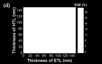
12 List of Figures Figure 1.1 Examples of commercial OLED devices; television (upper left; LG OLED TV), mobile phone adopting bendable OLED dispay (upper right; Samsung Galaxy S8), flexible OLED lighting and display devices are implemented for tail lamps in automobile (lower left; BMW M4, lower right; Audi)... 2 Figure 1.2 Schematic representation of TADF mechanism Figure 1.3 Potential energy diagram of exciplex formation and emission Figure 2.1 (a) Chemical structures of mcp, B3PYMPM and 4CzIPN. (b) Absorption spectrum of 4CzIPN and PL spectra of mcp:b3pympm film and mcp:b3pympm:5 wt% 4CzIPN film Figure 2.2 (a) Angle-dependent PL intensity of the p-polarized light from a 30-nm-thick film composed of mcp:b3pympm:5wt% 4CzIPN at 515 nm. Solid line represents the theoretical fit to the experimental data with the horizontal transition dipole ratio of (b) Molecular structure of 4CzIPN. An arrow indicates the orientation of the transition dipole moment of the molecule. (c) Schematic diagram of the device structure and energy levels (ev) of the devices. (d) Contour plot of the predicted maximum EQEs as function of the thickness of HTL and ETL for green fluorescent OLEDs under the assumption of negligible electrical loss and both singlet and triplet excitons are havested as light in the OLEDs. A star represents the highest EQE of 29.6% achieved in this study where the thicknesses of HTL and ETL are 65 and 50 nm, respectively Figure 2.3 (a) Current density voltage luminance characteristics of the OLED. Inset: Angular distribution of the EL intensity of the OLED. The solid line represents the Lambertian distribution. (b) EQE and power efficiency of the optimized OLED with the thicknesses of HTL and ETL of 65 and 50 nm, respectively Figure 2.4. Current density voltage luminance characteristics of OLEDs (a) according to the thickness of ETL with the fixed thickness of HTL at 65nm and (b) according to the thickness of x
13 HTL with the fixed thickness of ETL at 50nm. EQE and power efficiency of the OLEDs (c) according to the thickness of ETL with the fixed thickness of HTL at 65 nm and (d) according to the thickness of HTL with the fixed thickness of ETL at 50 nm Figure 2.5 Comparison of the experimental (circle) and simulated (dashed line) EQEs (a) as a function of the thickness of ETL with the fixed thickness of HTL at 65 nm, and (b) as a function of the thickness of HTL with the fixed thickness of ETL at 50 nm Figure 2.6 Efficiency roll-offs of the OLEDs in this work compared to the other reported OLEDs of 4CzIPN Figure 2.7 Comparison of the experimental (dashed line) and the simulated (colored contour) angle dependent p-polarized PL spectrum of the mcp:b3pympm:5 wt% 4CzIPN film Figure 2.8 Optimized geometry and direction of transition dipole moment from S 1 to S 0 of 4CzIPN along (a) X, Y direction (b) Y, Z direction Figure 3.1 (a) Chemical structures of mcp, PO15 and 2CzPN. (b) The absorption and PL spectra of 2CzPN measured in methylene chloride and the PL spectra of mcp, PO15, mcp:po15 and mcp:po15:5 wt% 2CzPN were measured with 50 nm thick films on 1 mm thick fused silica Figure 3.2 (a). The film PL spectra of mcp, PO15, 2CzPN, 50 wt% mcp: 50 wt% 2CzPN, 50 wt% PO15 : 50 wt% 2CzPN, and mcp:5 wt% 2CzPN, and the EL spectrum of the blue OLED. (b) PL spectra of mcp:5 wt% 2CzPN, PBCB2CZ:5 wt% 2CzPN and TCTA:5 wt% 2CzPN. The film PL spectra were measured using 50 nm thick films deposited on precleaned fused silica substrates. Monochromatic light with the wavelength of 250 nm~330 nm, considering 2nd harmonic, from a Xenon lamp was used as the excitation source and a photomultiplier tube as the detector. (b) PL spectra of mcp:5 wt% 2CzPN, PBCB2CZ:5 wt% 2CzPN and TCTA:5 wt% 2CzPN. With the selection of different hosts for 2CzPN, the PL spectra were different from solvatochromic effect due to CT characteristics of the TADF material Figure 3.3 (a) Angle-dependent PL intensity of the p-polarized light from a 30-nm-thick film xi
14 composed of mcp:po15:5 wt% 2CzPN. Solid line represents the theoretical fit to the experimental data with the horizontal transition dipole ratio of A continuous wave diode laser (405 nm, Edmund optics Inc.) was used as the excitation source and the incident angle of the excitation light was fixed at 45 º from the plane normal direction of substrate and the p- polarized emitted light was detected at 480 nm. (b) Transient PL decays of mcp:po15:5 wt% 2CzPN at room temperature. Inset: prompt fluorescence measured in the range of 0 to 10 ns after excitation Figure 3.4 (a) Schematic diagram of the device structure and energy levels (ev) of the device. (b) Contour plot of the predicted maximum EQE values as functions of the thickness of the p-htl and n-etl for blue fluorescent OLEDs under the assumption of negligible electrical loss and the assumption that both singlet and triplet excitons are harvested as light in the OLEDs. The star represents the highest EQE of 21.8% achieved in this study where the thicknesses of the HTL and ETL are 45 and 50 nm, respectively Figure 3.5 (a) Current density-voltage-luminance characteristics and (b) EQE of the blue fluorescent OLED. The reproducibility of the OLED is in the range of ±0.5 % EQE. Inset: EL spectrum of the OLED. (C) Comparison of the EQEs of the OLEDs of mcp:po15:5 wt% 2CzPN (This Work), mcp:5 wt% 2CzPN (This Work) and PO15:5 wt% 2CzPN (This Work). The EQEs of previously reported OLEDs of mcp:5 wt% 2CzPN and PPT:5 wt% 2CzPN are added for comparison. The device structures for the EMLs evaluated in this work are identical to the one addressed in the manuscript, except the EMLs Figure 3.6 Angle-dependent PL intensities of the p-polarized light from a 30-nm-thick films of mcp:po15:5 wt% 2CzPN and mcp:5 wt% 2CzPN. Solid line represents the theoretical fit to the experimental data with the horizontal transition dipole ratio of 0.70 and 0.69 for mcp:po15:5 wt% 2CzPN and mcp:5 wt% 2CzPN, respectively. A continuous wave diode laser (405 nm, Edmund optics Inc.) was used as the excitation source and the incident angle of the excitation light was fixed at 45º from the plane normal direction of substrate and the p-polarized emitted light was detected at 480 nm xii
15 Figure 4.1 (a) Chemical structure of DTPDDA. DFT calculation data: (b) Molecular structure of DTPDDA. (c) HOMO level at the phenyl-dibenzo azasiline unit. (d) LUMO level at the triphenyl triazine unit Figure 4.2 (a) The absorption spectrum of DTPDDA measured in toluene and PL spectra of DTPDDA in various solvents. Numbers in the brackets are the dielectric constants of the solvents. (b) The PL spectra of DTPDDA and TSPO1 measured in toluene and methylene chloride, espectively. The rest of the PL spectra of mcp, mcp:tspo1, mcp:dtpdda, TSPO1:DTPDDA and mcp:tspo1:16 wt% DTPDDA were measured with 50 nm thick films on 1 mm thick fused silicas. Inset: the chemical structures of two hosts used for EML, mcp and TSPO1. mcp:dtpdda, TSPO1:DTPDDA and mcp:tspo1:16 wt% DTPDDA showed the emission solely from DTPDDA without the emission from the hosts, indicating that energy transfer from the host molecules to the dopant is efficient in this system. The photoluminescent quantum yield (PLQY) of the mcp:tspo1:16 wt% DTPDDA film was 74 ± 2% Figure 4.3 (a) Prompt and delayed PL spectra of mcp:tspo1: 16 wt% DTPDDA at 35 K. Prompt and delayed components were collected at 20 ns and 300 μs, respectively. (b) Transient PL decays of mcp:tspo1:16 wt% DTPDDA film measured at 450 nm at temperature of 300 K and 35 K. Inset: Transient PL within the range of 0 to 50 ns after excitation. Red dotted line is the single exponential fitting with decay time of 11.8 ns for the prompt fluorescence Figure 4.4 (a) Schematic diagram of the device structure and energy levels (ev) of the device. (b) Contour plot of the predicted maximum EQEs as function of the thickness of HIL and EIL for blue fluorescent OLEDs. A star indicates the achieved EQE in this work Figure 4.5 (a) EL spectrum of the blue fluorescent OLED Inset : (top) the image of blue emission from the OLED. (bottom) A star denotes the CIE coordinate of the EL spectrum at (0.149, 0.197). (b) Current density-voltage-luminance characteristics of the OLED. Inset: Angular distribution of the EL intensity of the OLED. The solid line represents the Lambertian distribution. (c) EQE and power efficiency of the blue fluorescent OLED to current densities xiii
16 Figure 4.6 Angle-dependent PL intensities of the p-polarized light from 30-nm-thick films composed of mcp:tspo1:16 wt% DTPDDA at 465nm. Solid lines represent theoretical fits to the experimental data Figure 5.1 Chemical structure, molecular structure, HOMO and LUMO of the emitters Figure 5.2 PL spectra of (a) DTPPDDA, (b) SPDDA and (c) BDAPM in various solvents. Numbers in the brackets are the dielectric constants of the solvents. (d) PL spectra of the host of mcp:tspo1 and the emitters. Absorption and PL spectra of DTPPDDA, BDAPM and SPDDA were measured in toluene. PL spectra of mcp:tspo1 and mcp:tspo1:x wt% emitter were measured with 50 nm thick films on 1 mm thick fused silicas. Doping ratios were 8, 16 and 2 wt% for DTPPDDA, BDAPM and SPDDA, respectively Figure 5.3 Transient PL decays of (a) mcp:tspo1: 8 wt% DTPPDDA, (b) mcp:tspo1: 16 wt% BDAPM and (c) mcp:tspo1: 2 wt% SPDDA films measured at the peak wavelengths of each materials at temperature of 300 K and 18 K. Insets : Prompt and delayed PL spectra measured at 18K for the estimation of S 1 and T Figure 5.4 (a) Schematic diagram of the device structure and energy levels (ev) of the device. (b) EL spectra of the blue fluorescent OLEDs Inset:CIE coordinates of the OLEDs in this work compared to that of NTSC. (c) Current density-voltage-luminance characteristics of the OLEDs. (d) EQEs of the blue fluorescent OLEDs to current densities Figure 5.5 Contour plot of the predicted maximum EQEs as a function of the thickness of HIL and EIL for OLED device of (a)dtppdda (b)bdapm and (c)spdda. Stars indicate the achieved EQE in this work Figure 6.1 (a) Chemical structures of the materials used in this work. (b) Absorption and PL spectra of the materials Figure 6.2 (a) Time resolved PL spectra and (b) transient decays of all the samples for the EML. Inset of (b): transient decay mcp:0.5 wt% TBPe and mcp:6wt% DTPPDDA:0.5 wt% TBPe of xiv
17 from excitation to 260 nm Figure 6.3 (a) Device structure, (b) EL spectra, (c) J-V-L and (d) EQEs of the blue fluorescent OLEDs Figure 6.4 (a) J-V-L and (b) EQEs of the OLEDs of mcp:b3pympm:0.5 wt% TBPe, mcp:b3pympm:10 wt% DTPPDDA:0.5 wt% TBPe, mcp:b3pympm:10 wt% Ir(ppz)3:0.5 wt% TBPe and mcp:b3pympm:10 wt% Ir(ppz)3:10 wt% DTPPDDA:0.5 wt% TBPe Figure 6.5 Singlet and triplet energy levels of mcp,hfp 2 (Ir)pic, DTPPDDA and TBPe Figure 6.6 Transition dipole moment of TBPe measured with mcp:0.5 wt% TBPe film Figure 6.7 (a) singlet and triplet levels and (b) absorption and PL spectra of mcp: B3PYMPM, Ir(ppz) 3, DTPPDDA and TBPe i
18 Chapter 1. Introduction 1.1 Brief history of organic light-emitting diodes (OLEDs) Organic light emitting diodes (OLEDs) are the device that converts electrical energy to light on the recombination of hole and electron injected from anode and cathode. OLEDs separate them from other display and lighting devices for their distinctive features of high color purity, fast response time and superior applicability. OLEDs can easily incorporate with various products from mobile phone, television and even automobile because depending on substrate, OLEDs can be transparent and flexible. (Figure 1.1) This year of 2017 marks the 30 years of anniversary since OLEDs based on heterojunction was firstly introduced by C. W. Tang et. al. in 1987, consisted of a hole-transport layer (HTL) and an electron-transport layer (ETL). He later discovered host-guest system in OLED devices using Alq3 as a host material, transferrering energy to dopant, however the electroluminescence efficiency was low from only ~25% of the excitons leading to optical emission in those fluorescent light-emitting materials. 1 In 1998, M.A. Baldo et. al reported 100% internal quantum efficiency (IQE) from the OLED of phosphorescent material, where organometallic compound was utilized for harvesting triplet excitons from strong spin-orbit coupling. This research is often referred to create a base for commercializing OLEDs in industry. 2 As the commercialization of OLEDs become successful, the need for high electroluminescence (EL) efficiency grew, especially in fluorescent OLEDs. One of the milestones in this era was C. Adachi et. al reported highly efficient fluorescent OLEDs based on thermally activated delayed fluorescence (TADF) where reverse intersystem crossing (RISC) takes place to harvest triplet excitons for light emission, from small singlet-triplet splitting ( E ). 3-4 ST 1

, flexible OLED lighting and display devices are implemented")
19 Figure 1.1 Examples of commercial OLED devices; television (upper left; LG OLED TV), mobile phone adopting bendable OLED dispay (upper right; Samsung Galaxy S8), flexible OLED lighting and display devices are implemented for tail lamps in automobile (lower left; BMW M4, lower right; Audi). 2
20 1.2 Efficiency of OLEDs The efficiency of OLEDs can be judged by calculating photons per injected electrons, which is the external quantum efficiency (EQE) of OLEDs. The EQE can be described with internal quantum efficiency (IQE; int ), and out-coupling efficiency ( out ), and can be defined as the equation below, 5 int / q (, ) (, ) (1) EQE out S T eff PL out,where is the charge balance factor, S / T is the singlet-triplet exciton factor ( S / T =0.25 for fluorescent emitters and S / T=1 for phosphorescent emitters), and q eff is the effective radiative quantum yield of the emitter in the cavity structure. q eff is a function of the photoluminescence quantum yield (PLQY) of the emitter ( PL ), as well as the structure of the microcavity, including the position of the emission zone represented by (a factor related to the device structure). The out-coupling efficiency out is a function of and the proportion of horizontally oriented dipoles, ( p / p p ), where p and p are the fractions of horizontal and vertical dipoles, respectively. As additional triplet takes part into emission process, S / T can be increased, resulting in significant improvement of IQE in OLEDs. 3-4 Also, enhancing charge injection by n- or p- type dopants in the transport layers, 6-7 and achieving improved charge balance in emission layer (EML) can increase in charge balance leading to higher IQE. 3
21 1.3 Additional triplet harvest in fluorescent OLEDs Thermally Activated Delayed Fluorescence (TADF) On the electrical excitation, 25% of singlet and 75% of triplet excitons are formed on the recombination of injected charge carriers according to the spin statics. Therefore, phosphorescent material of metal-organic complex were used as sole means to harvest non-radiative triplet excitons. 2 However, even in metal-free fluorescent material, if singlet-triplet spitting ( small enough, then efficient spin-up conversion from non-radiative state to radiative singlet states can happen via reverse intersystem crossing (RISC) in thermally activated delayed fluorescence (TADF) material. 3 (see Figure 1.2) EST ) is The design rule for TADF material is the spatial separation of the highest occupied molecular orbital (HOMO) and the lowest unoccupied molecular orbital (LUMO), which forms intramolecular charge transfer (CT) state in a single molecule. Exchange energy decreases exponentially with increasing HOMO LUMO separation distance. From strong CT character of the TADF material, TADF material typically shows linear solvatochromic shift in photoluminescence (PL) spectra to the increase of dielectric constants of adopted solvents. From RISC, delayed emission is usually observed from TADF material, increasing as the increase of temperature. However, for some cases, non-radiative transition from triplet state was larger than RISC rate, therefore delayed emission was increased in the lowest temperature from suppressing non-radiative transition from triplet state. TADF materials are not only being used as emitters but also used as assisted dopants even host materials, taking advtantage of their small E ST. 8 Commercially, blue fluorescent OLEDs are being used in spite of low electroluminescence (EL) efficiency for poor stability and toxicity of blue phosphorescent OLEDs. Therefore, investigation of efficient blue TADF based OLEDs is necessary at this point. Recently, EQE over ~30% was reported in blue fluorescent OLED using TADF emitter, and separately deep blue emission was realized in the Commission Internationale de L Eclairage (CIE) coordinates of (0.149, 0.197) However, reports on simultaneously achieving both deep blue emission 4
22 (CIE(y)<0.2), and high EL efficiency in blue fluorescence OLEDs are scarce. Furthermore, emitting from TADF material expose drawbacks of broad EL spectrum deteriorating color purity and short device lifetime. 5

23 Figure 1.2 Schematic representation of TADF mechanism. 3 6
24 1.3.2 Intermolecular charge transfer complex (Exciplex) An excited intermolecular charge-transfer (CT) complex is the exciplex which is associated of differing molecule between electron-donating and electron-accepting molecules under photoand electrical excitation. The CT state occurs with the independent excited donor (D*) and an excited acceptor (A*) molecues. Exciplex is repulsive in ground state and attractive in excited state as shown in Figure 1.3. For complex consisted of the sam molecules referred to excited state dimer (excimer) which is a common phenonmenon for aromatic molecules especially if the singlet state lifetime is long. Since exciplex emission orginate from the lowest unoccupied molecular orbital (LUMO) of an acceptor and the highest occupied molecular orbital (HOMO) of a donor, newly formed HOMO-LUMO in exciplex contribute to small exchange energy which is proportional to the gap of singlet and triplet states ( E ST ). HOMO and LUMO of exciplex are located at two different molecules, therefore exciplex should have triplet level close to singlet level smaller than that of intramolecular CT material (TADF). Hence, reverse intersystem crossing (RISC) should be efficient in exciplex. Exciplex emission occurs following Frank-Condon principle, from the minimum of excited state to ground state. Therefore, photoluminescence (PL) spectrum of exciplex is red-shifted to those of donor and acceptor molecules and featurless from indefinite vibrational character of the ground state. 11 Previously reported OLEDs adopting exciplex system demonstrated efficient device performance in terms of external quantum efficiency (EQE), low driving voltage and efficiency roll-off from combined advantage of efficient energy transfer (ET) to dopant, charge balance and low exciton density due to broad recombination zone

25 Figure 1.3 Potential energy diagram of exciplex formation and emission. 8
26 1.4 Outline of the thesis In this thesis, we investigate fluorescent organic light emitting diodes (OLEDs) in order to realize high electroluminescence (EL) efficiency, especially blue fluorescent OLEDs. 100% internal quantum efficiency (IQE) was achieved with a green fluorescent OLED exhibiting 30% external quantum efficiency (EQE). The OLED comprises the exciplex-forming co-host system of N,N -dicarbazolyl-3,5-benzene (mcp) and bis-4,6-(3,5-di-3-pyridylphenyl)-2- methylpyrimidine (B3PYMPM) doped with the fluorescent dye of (4s,6s)-2,4,5,6-tetra(9Hcarbazol-9-yl)isophthalonitrile (4CzIPN) that has a strong delayed fluorescence as a result of reverse intersystem crossing (RISC). The exciplex-forming cohosts stimulate energy transfer and charge balance in the system. From using exciplex cohost, recombination zone was broad lowering exciton density, which showed the smallest efficiency roll-off among the OLEDs of 4CzIPN. The orientation of the transition dipole moment of the fluorescent dye was shown to have an influence on the EQE of the device. (Chapter 2) The mixed cohosts of mcp and 2,8-bis(diphenylphosphoryl)dibenzothiophene (PO15) have been developed for a highly efficient blue fluorescent OLED doped with a thermally activated delayed fluorescence (TADF) emitter [4,5-di (9H-carbazol-9-yl) phthalonitrile (2CzPN)]. We have demonstrated one of the highest external quantum efficiency of 21.8% in blue fluorescent OLEDs, which is identical to the theoretically achievable maximum EL efficiency using the emitter. Interestingly, the efficiency roll-off is large even under the excellent charge balance in the device and almost the same as the single host based devices, indicating that the efficiency rolloff in 2CzPN based TADF host is related to the material characteristics, such as low reverse intesystem crossing rate rather than charge imbalance. (Chapter 3) For electroluminescence with delayed fluorescence, the azasiline unit has been introduced for the first time as a donor in a TADF material. The TADF material of 5-(4-(4,6-diphenyl-1,3,5- triazin-2-yl)phenyl)-10,10-diphenyl-5,10-dihydrodibenzo[b,e][1,4]azasiline (DTPDDA) showed strong intramolecular charge transfer (CT) character with large spatial separation with the 9
27 acceptor of triazine leading to narrow splitting of singlet and triplet excited states for the efficient RISC. The blue organic light emitting diode (OLED) based on DTPDDA not only displays deep blue in the Commission Internationale de L Eclairage (CIE) coordinates of (0.149, 0.197) but also exhibits a high EQE of 22.3% which is the highest value ever reported for a blue fluorescent OLED. Theoretical prediction based on transient photoluminescence (PL) and optical simulation result agrees well with the achieved EQE indicating the successful conversion of triplet excitons to singlet in the blue fluorescent OLED by using DTPDDA. (Chapter 4) Further utilizing the azasiline unit, 5-(4 -(4,6-diphenyl-1,3,5-triazin-2-yl)-[1,1 -biphenyl]- 4-yl)-10,10-diphenyl-5,10-dihydrodibenzo[b,e][1,4]azasiline (DTPPDDA) in the formation of donor connector acceptor (D C A) materials resulted in deep blue emission with CIE coordinate of (0.151, 0.087), close to the blue standard of the National Television System Committee (NTSC) of (0.140, 0.080) with 4.7% EQE. In the donor acceptor donor (D A D) type materials of bis(4-(10,10-diphenyldibenzo[b,e][1,4]azasilin-5(10h)-yl)phenyl)methanone (BDAPM) and 5,5 -(sulfonylbis(4,1-phenylene))bis(10,10-diphenyl-5,10- dihydrodibenzo[b,e][1,4]azasiline) (SPDDA), carbonyl and sulfone units were used as the acceptors, respectively. The sulfonyl unit contributed to a large twist of the molecular structure while the carbonyl unit led to a small twist of the molecular structure. As a result, the blue fluorescent OLEDs containing BDAPM and SPDDA demonstrated 11.4% and 2.3% EQEs with CIE y-values of and 0.107, respectively. (Chapter 5) Almost all the triplets were harvested in the conventional blue fluorescence OLED using a blue fluorophore of 2,5,8,11-tetra-tert-butylperylene (TBPe) as the emitter by promoting both sensitizing and heavy atom effect (HAE) through co-doping TADF material of DTPPDDA and phosphorescent material of bis-2-(2,4-difluoro-3-(perfluoropropyl)phenyl)-4-methylpyridine-ir Ⅲ-picolinate ((HFP)2Ir(pic)) into emitting layer (EML). Comparison of the theoretical and experimental data indicates that the singlet to triplet ratio ( ) was increased from 0.23 to 0.94 S/ T with increased EQE from 5.6% to 12.3% in blue fluorescent OLED when the both TADF material 10
28 of DTPPDDA and phosphorescent material of (HFP)2Ir(pic) were doped together as assisted dopants. (Chapter 6) 11
29 Chapter 2. A Fluorescent Organic Light-Emitting Diode with 30% External Quantum Efficiency 2.1 Introduction Over the past two decades, phosphorescent organic light-emitting diodes (PhOLEDs) based on heavy metal complexes have been recognized as the sole solution for achieving 100% internal quantum efficiency (IQE) by harvesting both singlet and triplet excitons as light. Recently, however, fluorescent OLEDs showing a delayed emission without any heavy-metal complexes have attracted tremendous attention as a promising solution for simultaneously obtaining high external quantum efficiency (EQE), low cost, and stability of the device. 3-4,13,15,21-25 These fluorescent materials are able to harvest triplet excitons as well as singlet excitons under electrical excitation via reverse intersystem crossing (RISC) from the triplet (T 1 ) to singlet (S 1 ) state due to the low energy gap between the two states normally below 0.1 ev. Ideally, 100% IQE can be achieved, leading to around 30% EQE in the fluorescent OLEDs, if the efficiency of the RISC is unity. However, the highest reported EQE of the fluorescent OLEDs is below 20%, 25 which is still much lower than the ~30 35% EQE achieved by PhOLEDs. 5,12,26-34 In this article, a green fluorescent OLED with 30% EQE corresponding to almost 100% IQE is demonstrated. It comprises an exciplex-forming host doped with a fluorescent dye, (4s,6s)- 2,4,5,6-tetra(9H-carbazol-9-yl)isophthalonitrile (4CzIPN), which shows strong delayed fluorescence through RISC. The exciplex-forming host was introduced to stimulate energy transfer and charge balance in the system. 5, 12,28-30, In addition, the orientation of the transition dipole moment of the fluorescent dye influencing the EQE of the device will be discussed. 12
30 2.2 Experimental The OLEDs were fabricated on clean glass substrates pre-patterned with 70-nm-thick ITO under a pressure of Torr by thermal evaporation without breaking the vacuum. Before the deposition of organic layers, the ITO substrates were pre-cleaned with isopropyl alcohol and acetone, and then exposed to UV ozone for 10 minutes. Organic layers were deposited at a rate of 1 Å/s, and the deposition rate of co-deposited layers was 1 Å/s in total. Current density, luminance, and EL spectra were measured using a programmable source meter (Keithley 2400) and a spectrophotometer (Spectrascan CS100, Photo Research). The angular distribution of the EL was measured with a programmable source meter (Keithley 2400), goniometer, and fiber optic spectrometer (Ocean Optics S2000). The EQE and the power efficiency of the OLEDs were calculated from current density voltage luminance characteristics, EL spectra, and the angular distribution of the EL intensity. Geometry optimizations and calculations of the transition dipole moments of 4CzIPN were performed using B3LYP-level theory and the 6 31G(d) basis set for all the other atoms with Gaussian Orientation of the transition dipole moments was measured using a continuous wave diode laser (405 nm, Edmund optics Inc.). The incident angle of the excitation light was fixed at 45 from the plane normal direction of the substrate, and the p-polarized emitted light was detected at 515 nm, which is close to the peak wavelength of the PL spectrum of the fluorescent dye. Cyclic voltammetry was performed on a VSP versatile modular potentiostat, and data were analyzed using EC-LAB. A platinum wire was used as the counter-electrode, and a platinum disk was used as the working electrode. 13
31 2.3 Result and discussion N,N -dicarbazolyl-3,5-benzene (mcp) and bis-4,6-(3,5-di-3-pyridylphenyl)-2- methylpyrimidine (B3PYMPM) at a molar ratio of 1:1 were selected as the cohosts for 4CzIPN. Figure 2.1 shows the chemical structures of mcp, B3PYMPM, and 4CzIPN; the emission spectra of mcp:b3pympm and mcp:b3pympm:(5 wt% 4CzIPN) films; and the absorption spectrum of the 4CzIPN film. The cohost system efficiently formed an exciplex upon photo-excitation, manifested by a featureless photoluminescence (PL) spectrum, which was redshifted from the spectra of mcp and B3PYMPM. 33 The normalized PL spectrum of the mcp:b3pympm film doped with 5 wt% 4CzIPN showed emission entirely from 4CzIPN with the peak position at 515 nm (optical energy gap of 2.58 ev), 3 indicating that the energy transfer from the exciplex to the fluorescent dopant is efficient. The efficient energy transfer is expected from the large spectral overlap between the exciplex emission and the absorption of 4CzIPN. The photoluminescent quantum yield (PLQY) of the mcp:b3pympm:(5 wt% 4CzIPN) film was 97 ± 3%; it was measured in an integrating sphere using a He Cd laser (325 nm) as an excitation source. 35 The PLQY value is close to that reported in the literature. 3 Almost 100% PLQY of the mcp:b3pympm:(5 wt% 4CzIPN) film is attributed to the efficient energy transfer from the host to 4CzIPN and the efficient blocking of the non-radiative decay processes of the excited states of 4CzIPN. 14
 Chemical structures of")
 Absorption spectrum of")

32 Figure 2.1 (a) Chemical structures of mcp, B3PYMPM and 4CzIPN. (b) Absorption spectrum of 4CzIPN and PL spectra of mcp:b3pympm film and mcp:b3pympm:5 wt% 4CzIPN film. 15


33 16
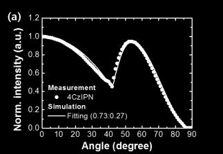
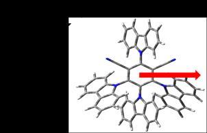
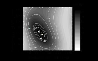
34 Figure 2.2 (a) Angle-dependent PL intensity of the p-polarized light from a 30-nm-thick film composed of mcp:b3pympm:5wt% 4CzIPN at 515 nm. Solid line represents the theoretical fit to the experimental data with the horizontal transition dipole ratio of (b) Molecular structure of 4CzIPN. An arrow indicates the orientation of the transition dipole moment of the molecule. (c) Schematic diagram of the device structure and energy levels (ev) of the devices. (d) Contour plot of the predicted maximum EQEs as function of the thickness of HTL and ETL for green fluorescent OLEDs under the assumption of negligible electrical loss and both singlet and triplet excitons are havested as light in the OLEDs. A star represents the highest EQE of 29.6% achieved in this study where the thicknesses of HTL and ETL are 65 and 50 nm, respectively. 17
35 Since 4CzIPN shows strong delayed fluorescence, efficient triplet harvesting is also expected by RISC with negligible triplet loss. The higher T 1 levels of mcp, B3PYMPM, and the exciplex of mcp:b3pympm that is, 2.90, 2.68, and 2.97 ev, respectively, 33 higher than that of 4CzIPN with a T 1 level = 2.50 ev guarantees efficient exciton confinement to 4CzIPN and prohibits backward energy transfer from 4CzIPN to the host materials. Orientation of the transition dipole moment of 4CzIPN in the mcp:b3pympm:(5 wt% 4CzIPN) film was measured using the angle-dependent p-polarized PL spectrum of the mcp:b3pympm:(5 wt% 4CzIPN) film on a fused silica substrate to simulate the outcoupling efficiency and optimum device structure. 5,32,36-38 The angle-dependent PL intensity was consistent with the horizontal transition dipole ratio (Θ) of 0.73 for 4CzIPN as shown in Figure 2.2a, where Θ is defined as the ratio of the horizontal portion of the dipoles to the total dipoles. Geometry optimization in the ground state and the transition dipole moment of the 4CzIPN molecule were further calculated using density functional theory (DFT) and time-dependent DFT to elucidate the orientation of the molecule. The calculation showed that the molecule has a flat planar structure along the x and y direction as shown in Figure 2.2b. This shape of the molecule typically enables stacking parallel to the substrate. In addition, the transition dipole moment of 4CzIPN is parallel to the x and y directions, leading to the strong preferred orientation parallel to the substrate. Based on the measured values of Θ = 0.73 and PLQY = 0.97 for 4CzIPN, optical simulation was performed under the assumption of negligible electrical loss to predict the maximum achievable EQE of the fluorescent OLEDs as a function of the thickness of the hole-transporting layer (HTL) and electron-transporting layer (ETL). 5 Both singlet and triplet excitons are also assumed to be harvested as light. The device structure used in the simulation was ITO (indium tin oxide, 70 nm)/mcp (X nm)/mcp:b3pympm:(5 wt% 4CzIPN) (30 nm)/b3pympm (Y nm)/al (100 nm), as shown in Figure 2.2c. Figure 2.2d shows that a 29.3% EQE is achievable in the fluorescent OLED with 4CzIPN in the case of X = 65 nm and Y = 50 nm. The star in the EQE contour plot represents the highest experimental data actually achieved in this study. The structure of the fabricated device was slightly modified from the simulated one by 18
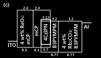
36 inserting a hole-injection layer (HIL; p-doped mcp) and an electron-injection layer (EIL; n-doped B3PYMPM) to demonstrate the efficient charge injection The device structure (Figure 2.2c) is as follows: ITO ( 70 nm)/(4 wt% ReO 3 ):mcp (A nm)/mcp (15 nm)/mcp:b3pympm:(5 wt% 4CzIPN) (30 nm)/b3pympm (20 nm)/(4 wt% Rb 2 CO 3 ):B3PYMPM (B nm)/al (100 nm). The values used for the thicknesses of the HTL and ETL in the simulation (X and Y nm) correspond to the sum of the thickness of the p- or n-doped layers (A or B nm) and the intrinsic charge transporting layers (15 nm); this can be explained as follows: A nm + 15 nm = X nm for HTL and B nm + 15 nm = Y nm for ETL. 19
 Current density voltage luminance")


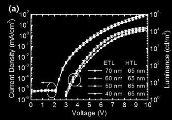
37 Figure 2.3 (a) Current density voltage luminance characteristics of the OLED. Inset: Angular distribution of the EL intensity of the OLED. The solid line represents the Lambertian distribution. (b) EQE and power efficiency of the optimized OLED with the thicknesses of HTL and ETL of 65 and 50 nm, respectively. 20
38 Table 2.1 The voltage, current efficiency, EQE and power efficiency of the OLED. Voltage [V] Current Efficiency [cd/a] EQE [%] Power Efficiency [lm/w] Turn on 1,000 cd/m 2 10,000 cd/m 2 Max. 1,000 10,000 cd/m 2 cd/m 2 Max. 1,000 cd/m 2 10,000 cd/m 2 Max. 1,000 cd/m 2 10,000 cd/m
39 The highest occupied molecular orbital (HOMO) level of 4CzIPN was defined as 5.7 ev based on the cyclic voltammetry (CV) measurements, and the lowest unoccupied molecular orbital (LUMO) was 3.12 ev. Figure 2.3a and b shows the current density voltage luminance (J V L) characteristics and the calibrated efficiencies of the optimized fluorescent OLED, respectively. The factor used for the calibration of efficiency was 1.02, which was obtained from a pattern that is broader than the Lambertian curve on the angular distribution of the electroluminescence (EL) intensity of the OLED as shown in the inset of Figure 2.3a. The turn-on voltage of the OLED was 3.0 V, and a luminance of 1000 cd/m 2 was obtained at 5.6 V. The device surprisingly exhibited a high maximum EQE of 29.6% and a maximum current efficiency of 94.5 cd/a, which is consistent with the simulation results. The efficiencies are by far the highest values achieved for fluorescent OLEDs, and they are very close to the highest efficiencies of PhOLEDs reported up to now. However, the efficiency roll-off is large with EQE values of 27.8% at 1000 cd/m 2 and 14.5% at cd/m 2, probably due to large triplet triplet annihilation coming from the long triplet exciton lifetime of 4CzIPN. The voltage, current efficiency, EQE, and power efficiency of the OLED at different luminance values are sorted in Table 1. The origin of the large efficiency rolloff is currently under investigation and will be reported separately. To validate the device simulation results shown in Figure 2.2c, seven different fluorescent OLEDs with different HTL and ETL thicknesses (X,Y) were fabricated, and the device performance values are provided in Figure 2.4. Figure 2.5a and b compare the experimentally obtained EQEs with the simulation results at fixed thicknesses of HTL and ETL, respectively. As expected, the efficiencies are more sensitive to the thickness variation of the ETL than that of the HTL because of the interference effect of the reflected light from the cathode. Both figures show that the achieved maximum EQEs of the OLEDs with different ETL and HTL thicknesses agree very well with predicted theoretical EQEs within an uncertainty range of ±2% for Θ and ±3% for PLQY, where the electrical loss could be assumed to be negligible in the devices. Hence, it is very 22
40 clear that the EQE that is close to the theoretical limit has been achieved in the fluorescent OLEDs harvesting all the singlet and triplet excitons without electrical loss. Efficiency roll-offs of the OLEDs in this study was the smallest among the reported OLEDs of 4CzIPN, from low exciton density owing to large recombination zone of exciplex. (Figure 2.6) 23

41 24

 according to")


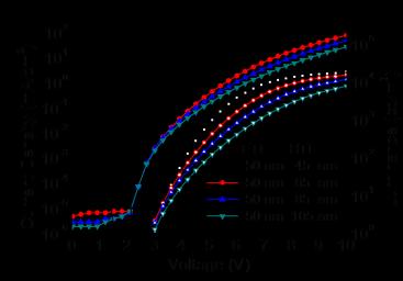
42 Figure 2.4. Current density voltage luminance characteristics of OLEDs (a) according to the thickness of ETL with the fixed thickness of HTL at 65nm and (b) according to the thickness of HTL with the fixed thickness of ETL at 50nm. EQE and power efficiency of the OLEDs (c) according to the thickness of ETL with the fixed thickness of HTL at 65nm and (d) according to the thickness of HTL with the fixed thickness of ETL at 50nm. 25
 and simulated (dashed")
 as a function of the")
43 Figure 2.5 Comparison of the experimental (circle) and simulated (dashed line) EQEs (a) as a function of the thickness of ETL with the fixed thickness of HTL at 65 nm, and (b) as a function of the thickness of HTL with the fixed thickness of ETL at 50 nm. 26

44 Figure 2.6 Efficiency roll-offs of the OLEDs in this work compared to the other reported OLEDs of 4CzIPN
 and the simulated (colored contour)")
45 Figure 2.7 Comparison of the experimental (dashed line) and the simulated (colored contour) angle dependent p-polarized PL spectrum of the mcp:b3pympm:5 wt% 4CzIPN film. 28


 X, Y direction (b)")
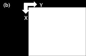
46 Figure 2.8 Optimized geometry and direction of transition dipole moment from S 1 to S 0 of 4CzIPN along (a) X, Y direction (b) Y, Z direction. 29
47 2.4 Conclusion In summary, we have demonstrated a green fluorescent OLED with a maximum EQE of 30%, which corresponds to almost 100% IQE, using 4CzIPN as the emitter in an exciplexforming cohost system composed of mcp and B3PYMPM. The EQE is very close to the highest values for PhOLEDs, indicating that the fluorescent OLED harvested not only all the singlet excitons but also all the triplet excitons via RISC without electrical loss. The results clearly demonstrate that fluorescent OLEDs can perform as well as PhOLEDs. 30
48 Chapter 3. A highly efficient sky-blue fluorescent organic light emitting diode based on mixed co-host system for thermally activated delayed fluorescence emitter (2CzPN) 3.1 Introduction Thermally activated delayed fluorescence (TADF) draws more and more attention because of its capacity to harvest triplet excitons to light in organic light emitting diodes (OLEDs). Blue emitting TADF materials and devices are especially attractive because low efficiency fluorescent molecules are in use in commercial products. Many efficient blue fluorescent OLEDs based on TADF materials have been reported including the report with the high external quantum efficiency (EQE) of 20.6%. 3,25,46-53 However, it is under question if the potential of the blue TADF emitters have been fully materialized in terms of efficiency. For example, 4,5-di (9H-carbazol-9- yl) phthalonitrile (2CzPN) which is known as an efficient TADF material emitting sky-blue showed the EQE of 13.6% although 2CzPN has a high photoluminescence quantum yield (PLQY) over 85%. The EQE of the device must be higher than the reported value if the triplets in OLEDs are sufficiently converted to singlet excitons. In addition to the development of the TADF materials with good color purity, good stability, and high photoluminescence quantum yield, selection of a proper host and charge transporting materials along with the optimization of device structures are required to fully capitalize the potential of the materials by achieving good electrical balance and maximizing outcoupling efficiency. Double emitting layers, bipolar hosts, mixed hosts, and exciplex forming hosts instead of hole or electron transporting single hosts have been developed to realize good charge balance without electrical loss in conventional fluorescent and phosphorescent OLEDs. 28,54-58 However, most of blue TADF OLEDs adopted single hosts probably because of the difficulties in selecting host materials satisfying the requirements of high triplet levels, the low energy barrier for charge injection from electron and hole transporting layers and balanced electron and hole 31
49 mobilities. 3,25,46-50 Through ambipolar transport of a mixed host in emitting layer (EML), charge balance can be improved in OLEDs. In this study, we have developed a mixed host consisting of a hole transporting material and an electron transporting materials for blue TADF OLEDs and demonstrated a highly efficient blue fluorescent OLED with 21.8% of EQE using 2CzPN as the TADF dopant in a mixed host. It is one of the most efficient blue fluorescent OLEDs. Additionally, theoretical calculation revealed that the EQE of 21.8% is indeed the maximum achievable efficiency using 2CzPN as the blue dopant, indicating that the mixed host gives little electrical loss and efficient triplet harvesting to realize efficient blue OLEDs in general. Origin of efficiency roll-off in 2CzPN based TADF OLEDs will be discussed by comparing the characteristics between the OLEDs of the different hosts. 32
50 3.2 Experimental The OLEDs were fabricated on clean glass substrates pre-patterned with 70- nm -thick ITO under a pressure of Torr by thermal evaporation without breaking the vacuum. Before the deposition of organic layers, the ITO substrates were pre-cleaned with isopropyl alcohol and acetone, and then exposed to UV ozone for 10 minutes. Organic layers were deposited at a rate of 1 Å/s, and the deposition rate of co-deposited layers was 1 Å/s in total. Current density, luminance, and EL spectra were measured using a programmable source meter (Keithley 2400) and a spectrophotometer (Spectrascan CS100, Photo Research). The angular distribution of the EL was measured with a programmable source meter (Keithley 2400), goniometer, and fiber optic spectrometer (Ocean Optics S2000). The EQE and the power efficiency of the OLEDs were calculated from current density voltage luminance characteristics, EL spectra, and the angular distribution of the EL intensity. Orientation of the transition dipole moments was measured using a continuous wave diode laser (405 nm, Edmund optics Inc.). The incident angle of the excitation light was fixed at 45 from the plane normal direction of the substrate, and the p-polarized emitted light was detected at 470 nm, which is close to the peak wavelength of the PL spectrum of the fluorescent dye. Cyclic voltammetry was performed on a VSP versatile modular potentiostat, and data were analyzed using EC-LAB. A platinum wire was used as the counter-electrode, and a platinum disk was used as the working electrode. PL spectra of the organic materials were measured using samples thermally deposited on fused silica under a vacuum of Torr. The samples were excited with a He/Cd laser (325 nm) to detect PL using a photomultiplier tube attached to a monochromator. Transient PL was measured by using a pulsed N 2 laser (KEN-2X, USHO) as the excitation light source and a streak camera (C10627, Hamamatsu) as the optical detection system. 33
51 3.3 Result and discussion 1,3-Bis(N-carbazolyl)benzene (mcp) and 2,8- bis(diphenylphosphoryl)dibenzothiophene (PO15) were selected as the cohosts for EML with the molar ratio of 1:1 for 2CzPN considering their higher singlet and triplet energies than those of 2CzPN to prevent the triplet excited state of 2CzPN from quenching by triplet energy transfer to the host molecules. 33,59 The molecular structures of the materials are shown in Figure 3.1a. The absorption spectrum of 2CzPN and photoluminescence (PL) spectra of all the materials used in this work are shown in Figure 3.1b. The UV vis absorption spectrum of 2CzPN was measured in methylene chloride (MC) using a UV vis NIR spectrophotometer (Agilent, Cary-5000). The photoluminescence spectra of the materials except 2CzPN were measured using 50 nm thick films deposited on precleaned fused silica substrates. Monochromatic light with the wavelength of 250 nm from a xenon lamp was used as the excitation source and a photomultiplier tube as the detector (Photon Technology International). Large overlap of the emission spectra of the mixed cohosts of mcp:po15 with the absorption spectrum of 2CzPN and the almost identical PL spectrum of the 2CzPN doped (5 wt %) mixed host film with the PL of the 2CzPN indicate that the energy transfer from the hosts to the TADF dopant takes place in the doped EML. Neither mcp nor PO15 forms an exciplex with 2CzPN as manifested in Figure 3.2a and 3.2b. 34
 The absorption and PL spectra of 2CzPN measured in methylene chloride and the PL spectra of mcp, PO15, mcp:po15 and mcp:po15:5")
52 Figure 3.1 (a) Chemical structures of mcp, PO15 and 2CzPN. (b) The absorption and PL spectra of 2CzPN measured in methylene chloride and the PL spectra of mcp, PO15, mcp:po15 and mcp:po15:5 wt% 2CzPN were measured with 50 nm thick films on 1 mm thick fused silica. 35
 PL spectra of mcp:5 wt% 2CzPN, PBCB2CZ:5 wt% 2CzPN and TCTA:5 wt% 2CzPN. The film PL spectra were measured using 50 nm thick films deposited on precleaned fused silica substrates.")
53 Figure 3.2 (a). The film PL spectra of mcp, PO15, 2CzPN, 50 wt% mcp: 50 wt% 2CzPN, 50 wt% PO15 : 50 wt% 2CzPN, and mcp:5 wt% 2CzPN, and the EL spectrum of the blue OLED. (b) PL spectra of mcp:5 wt% 2CzPN, PBCB2CZ:5 wt% 2CzPN and TCTA:5 wt% 2CzPN. The film PL spectra were measured using 50 nm thick films deposited on precleaned fused silica substrates. Monochromatic light with the wavelength of 250 nm~330 nm, considering 2nd harmonic, from a Xenon lamp was used as the excitation source and a photomultiplier tube as the detector. With the selection of different hosts for 2CzPN, the PL spectra were different from solvatochromic effect due to CT characteristics of the TADF material. 36
54 The PL spectra shift of 2CzPN in the different hosts must come from solvatochromic effect due to charge transfer (CT) nature of the TADF material of 2CzPN. The weak emission from the host near the wavelength of 425 nm indicates that the energy transfer from the host to 2CzPN is not 100% in the EML on photoexcitation, however under electrical excitation as shown later, the host emission disappeared in the EL spectrum due to direct charge trapping on the dopant in addition to energy tranfer. The PLQY and the orientation of the transition dipole moment of 2CzPN molecules in the mcp:po15:5 wt % 2CzPN film were measured using an integrating sphere and from the angle dependent PL spectra, respectively The PLQY of mcp:po15:5 wt % 2CzPN was 84 ± 2% which is close to the reported one. 46 The horizontal emitting dipole ratio was 70% as shown in Figure 3.3a. The transient PL from the mcp:po15:5 wt % 2CzPN showed that multiexponential decays fitted well with the prompt lifetime of 16 ns and four delayed lifetimes of 36 ns, 7 μs, 226 μs, and 897 μs (Figure 3.3b), which was measured using a streak camera (C4334, Hamamatsu Photonics) excited by a nitrogen gas laser at a wavelength of 337 nm with a pulse width of 500 ps (MNL200, Lasertechnik). The reason for the four components in the transient decay is not clear yet, and it is under investigation now. The portion of the prompt and the delayed emission intensity in PL calculated from the transient PL decay at room temperature (RT) was 0.62:0.38, resulting in the total, prompt, and delayed PLQYs of 84%, 52%, and 32%, respectively. Maximum achievable internal quantum efficiency (IQE) of OLEDs using the dye can be calculated by considering PLQYs and reverse intersystem crossing (RISC) efficiency (80%). 46 Maximum achievable IQE of the OLEDs was estimated to be 74%. The structure of the OLED based on the emitting layer was optimized theoretically to maximize the outcoupling efficiency using the classical dipole model. 5 The device structure shown in Figure 3.4a was used for the simulation with the experimentally determined PLQY and horizontal portion of transition dipole moment of the 2CzPN in the emitting layer. mcp and PO15 were used not only as the cohosts but also as the hole transporting layer (HTL) and electron 37
55 transporting layer (ETL) in the device, respectively, to remove the charge injection barriers from the charge transporting layers to the EML. The p-doped HTL (4 wt % ReO3:mCP layer) and the n-doped ETL (4 wt % Rb2CO3:PO15 layer) were inserted as the hole and electron injection layers in the device to enhance charge injection from the electrodes to the HTL and ETL, respectively The thickness of the p-htl and n-etl were systematically varied to find the optimum thicknesses to calculate the EQEs with the fixed thickness of 15 nm for the HTL, ETL and EML. Maximum outcoupling efficiency of 29.4% was predicted when the thicknesses of the p-htl and n-etl were 45 and 50 nm, respectively (Figure 3.4b). Combined with the estimated IQE of 74%, the maximum achievable EQE was predicted to be 21.8% for this OLED under assumption of little electrical loss (charge balance factor =1). 5 38
56 Figure 3.3 (a) Angle-dependent PL intensity of the p-polarized light from a 30-nm-thick film composed of mcp:po15:5 wt% 2CzPN. Solid line represents the theoretical fit to the experimental data with the horizontal transition dipole ratio of A continuous wave diode laser (405 nm, Edmund optics Inc.) was used as the excitation source and the incident angle of the excitation light was fixed at 45 º from the plane normal direction of substrate and the p- polarized emitted light was detected at 480 nm. (b) Transient PL decays of mcp:po15:5 wt% 2CzPN at room temperature. Inset: prompt fluorescence measured in the range of 0 to 10 ns after excitation. 39
 Contour plot of the predicted maximum EQE values as functions of the thickness of the p-htl and n-etl for blue fluorescent OLEDs under the assumption of negligible electrical loss and the")
57 Figure 3.4 (a) Schematic diagram of the device structure and energy levels (ev) of the device. (b) Contour plot of the predicted maximum EQE values as functions of the thickness of the p-htl and n-etl for blue fluorescent OLEDs under the assumption of negligible electrical loss and the assumption that both singlet and triplet excitons are harvested as light in the OLEDs. The star represents the highest EQE of 21.8% achieved in this study where the thicknesses of the HTL and ETL are 45 and 50 nm, respectively. 40
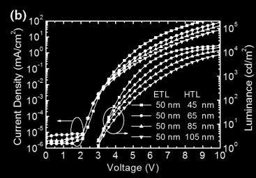
58 The current density voltage luminance characteristics of the OLED are shown in Figure 3.5a. The turn-on voltage of the OLED was 3.0 V, which is comparable to those of previously reported efficient blue fluorescent OLEDs and the driving voltage at 1000 cd/m2 was 6.4 V. 3,25,46-50 The device emits sky blue fluorescence with the Commission Internationale de L Eclairage (CIE) coordinates of (0.17, 0.27) and with the peak wavelength of 480 nm which was 7 nm redshifted from the PL spectrum due to the cavity effect of the device (inset of Figure 3.5b). The device exhibited the EQE of 21.8% (Figure 3.5b), which is much higher than the previously reported 13.6% obtained from the device using 2CzPN doped in a single host. 46 Furthermore, the OLED using the mixed cohost of mcp:po15 demonstrated higher EL efficiency than the OLEDs of single hosts of mcp and PO15 as shown in Figure 3.5c. Since the PLQYs and horizontal dipole ratios of 2CzPN in the single host of mcp and the mixed cohosts (Figure 3.6) are almost the same, EL efficiency of the blue fluorescent OLED was boosted by improved electron and hole balance achieved by adopting the mixed cohosts with optimized device structure. The experimentally obtained EQE was identical to the theoretically calculated maximum achievable EQE, indicating that this fluorescent OLED based on the mixed cohosts showed little electrical loss. As shown in Figure 3.5c, the comparison of roll-offs of this work to the previously reported OLEDs shows that the roll-offs of the OLEDs using 2CzPN are rather large. Large efficiency rolloffs in the OLED with the mixed host possessing excellent charge balance indicates that the rolloffs originate from quenching of excitons such as singlet triplet annihilation (STA) and triplet triplet annihilation (TTA) due to the slow RISC rate of 2CzPN rather than electron hole imbalance. Therefore, a TADF material with high singlet radiative rate and high RISC rate to lower triplet density should be synthesized to improve the efficiency roll-offs in blue TADF OLEDs. 41
59 Figure 3.5 (a) Current density-voltage-luminance characteristics and (b) EQE of the blue fluorescent OLED. The reproducibility of the OLED is in the range of ±0.5 % EQE. Inset: EL spectrum of the OLED. (C) Comparison of the EQEs of the OLEDs of mcp:po15:5 wt% 2CzPN (This Work), mcp:5 wt% 2CzPN (This Work) and PO15:5 wt% 2CzPN (This Work). The EQEs of previously reported OLEDs of mcp:5 wt% 2CzPN and PPT:5 wt% 2CzPN are added for 42
60 comparison. The device structures for the EMLs evaluated in this work are identical to the one addressed in the manuscript, except the EMLs. 3,46 43
61 Figure 3.6 Angle-dependent PL intensities of the p-polarized light from a 30-nm-thick films of mcp:po15:5 wt% 2CzPN and mcp:5 wt% 2CzPN. Solid line represents the theoretical fit to the experimental data with the horizontal transition dipole ratio of 0.70 and 0.69 for mcp:po15:5 wt% 2CzPN and mcp:5 wt% 2CzPN, respectively. A continuous wave diode laser (405 nm, Edmund optics Inc.) was used as the excitation source and the incident angle of the excitation light was fixed at 45º from the plane normal direction of substrate and the p-polarized emitted light was detected at 480 nm. 44
62 Table 3.1 Voltage, current efficiency, current density, EQE, and power efficiency of the OLED. Turn on /Max. 1,000 cd/m 2 2,000 cd/m 2 Voltage [V] Current Density [ma/cm 2 ] Current Efficiency [cd/a] EQE [%] Power Efficiency [lm/w]
63 3.4 Conclusion In summary, we have demonstrated a highly efficient blue fluorescent OLED with the EQE of 21.8% using the mixed cohosts of mcp:po15 doped with 2CzPN. Theoretical calculation showed that the blue fluorescent OLED with the mixed host used in this work pushed the device performance toward the theoretical limit by fullly utilizing the ability of the dopant. Efficiency roll-off is very large even in the OLED with excellent charge balance, indicating that the roll-off originates from the exciton quenching probably coming from low RISC of triplet exciton rather than charge imbalance. TADF materials with large RISC rates are required to reduce the efficiency roll-off. 46
64 Chapter 4. Thermally activated delayed fluorescence from azasiline based intramolecular charge-transfer emitter (DTPDDA) and a highly efficient blue light emitting diode 4.1 Introduction Enhancing electroluminescence (EL) efficiency might be a never ending pursuit from displays to lightings where organic light emitting diodes (OLEDs) are being used. In the past years, phosphorescent OLEDs (PhOLEDs) based on heavy metal complexes have been considered as an only solution to realize high efficiencies by harvesting both singlet and triplet excitons as light. 5,12,28,31,33-34,63 However, recently reported OLEDs utilizing delayed fluorescence challenged the conventional idea of achieving high EL efficiencies and have demonstrated an equal performance to PhOLEDs by achieving 30% external quantum efficiency (EQE). 3,13,58,61 There are two different mechanisms that drive delayed fluorescence, which are triplet triplet annihilation (TTA) and thermally activated delayed fluorescence (TADF) Fluorescent materials showing TADF enables additional harvest of triplet excitons as well as singlet excitons to light via thermally activated reverse intersystem crossing (RISC) from triplet (T 1 ) to singlet (S 1 ) state due to small charge transfer singlet triplet state splitting (ΔE ST ). Replacing phosphorescent materials by efficient TADF materials will eventually lower cost with the potential of clearing stability issues. Especially, blue dyes among the three primary colors have been considered as the most crucial ones due to their important role in generating white light with good color purity. So far, blue fluorescent materials are being used for commercial OLEDs in spite of their low efficiency due to short device lifetime of phosphorescent blue OLEDs. Even with such importance, there are only a few reports on efficient blue TADF materials which meet both the high EL efficiency and color purity up to now. TADF materials are charge transfer (CT) type emitters which are composed of electron donating and accepting units to have small but a certain degree of overlap between the highest occupied molecular orbital 47
65 (HOMO) and the lowest unoccupied molecular orbital (LUMO) to minimize the singlet triplet energy gap yet to still have large enough radiative transition rate. Carbazole and dimethyl dihydroacridine have been mainly used as the donor moieties and sulfone oxide and triazine as the acceptor unit in the blue TADF molecules. However, it seems quite challenging to search for an appropriate combination of donor and acceptor moieties to achieve good color purity and high EL efficiency for blue fluorescent OLEDs at the same time. Even a highly efficient blue fluorescent OLED of 20.6% was reported recently, yet the OLED displayed sky-blue light with the CIE coordinates of (0.19, 0.35). The highest EQE ever reported in deep blue fluorescent OLEDs, in terms of CIE-y value below 0.2, was 19.5%, which is still lower than the achieved EQE in this work. 25,47-49,66 In this article, we have utilized a new donor unit of the azasiline group to synthesize a deep blue TADF dye, 5-(4-(4,6-diphenyl-1,3,5-triazin-2-yl)phenyl)-10,10-diphenyl-5,10- dihydrodibenzo[b,e][1,4]azasiline (DTPDDA). An efficient blue fluorescent OLED with an unprecedented high EQE of 22.3% was fabricated by doping the TADF material in a mixed cohost system. The device emitted deep blue with the CIE coordinates of (0.149, 0.197). The comparison with the theoretical prediction of the EQE indicated that the RISC is efficient in the molecule to convert almost all the triplet excitons to the singlet excitons, and the device has little electrical loss. 48
66 4.2 Experimental The material of DTPDDA was synthesized in the department of chemistry and research institute for green energy convergence technology (RIGET) of Gyeongsang National University supervised by professor Yun-Hi Kim. Geometry optimization and energy level of HOMO and LUMO were calculated through DFT calculations with B3LYP level of theory, the 6-31G(d) basis set for all the atoms without solvent model and singlet and triplet energies, which were performed with TD-DFT calculations with Gaussian Detailed information on the optimized molecular geometry is addressed in Table 4.2. Organic films for the measurement of the PLQY and PL spectra were fabricated by thermal evaporation on precleaned quartz substrates at a base pressure of < Torr. The PLQY was measured by using an integrating sphere. A continuous-wave He/Cd laser (325 nm) was used as an excitation light source and a monochromator-attached photomultiplier tube (PMT) was used as an optical detection system. The PL spectra were also measured by PMT with a xenon lamp (260 nm) as an excitation light source. Transient and time resolved PL spectra were measured using a streak camera (C10627, Hamamatsu Photonics) excited by a nitrogen gas laser with a pulse width of 800 ps (KEN-2X, Usho). Orientation of transition dipole moments was measured using a continuous wave diode laser (405 nm, Edmund optics Inc.). The incident angle of the excitation light was fixed at 45 from the plane normal direction of substrate, and the p-polarized emitted light was detected at 465 nm that is close to the peak wavelength of the PL spectrum of the fluorescent dye. The OLEDs were fabricated on clean glass substrates prepatterned with 70-nm-thick ITO under a pressure of Torr by thermal evaporation without breaking the vacuum. Before the deposition of organic layers the ITO substrates were precleaned with isopropyl alcohol and acetone and then exposed to ultraviolet (UV) ozone for 10 min. Organic layers were deposited at 49
67 a rate of 1 Å/s, and the deposition rate of the codeposited layers was 1 Å/s in total. Current density, luminance, and EL spectra were measured using a programmable source meter (Keithley 2400) and a spectrophotometer (Spectrascan PR650, Photo Research). The angular distribution of the EL was measured with a programmable source meter (Keithley 2400), goniometer, and fiber optic spectrometer (Ocean Optics S2000). The EQE and the power efficiency of the OLEDs were calculated from J V L characteristics, EL spectra, and the angular distribution of the EL intensity. 50
68 4.3 Result and discussion Prior to synthesis of the blue fluorescent material with the chemical structure described in Figure 4.1a, the quantum chemical properties of the molecule have been investigated through the density functional theory (DFT) calculation. First, the geometry optimization (Figure 4.1b) and the energy levels of the compound and Kohn Sham orbitals of the HOMO (Figure 4.1c) and the LUMO states (Figure 4.1d) were calculated through the DFT calculation. Then, singlet and triplet energies of DTPDDA were calculated with optimized geometry using the time-dependent(td)- DFT. The details of the calculation method are explained in the Experimetal Section. The result showed that the HOMO and LUMO of DTPDDA are separated distinctively on two different units, the phenyl-dibenzo azasiline and the triphenyl triazine, respectively, by distorting of the dihedral angle. The TD-DFT calculation predicted the ΔE ST of 0.01 ev, indicating that the separation of Kohn Sham orbitals of HOMO and LUMO lowered the exchange energy to enhance the RISC. However, the HOMO and LUMO levels were weakly overlapped in the phenyl unit, which is known to increase radiative transition rate. 3 As the HOMO of DTPDDA is distributed over the azasiline unit while the LUMO resides at the triphenyl triazine unit at the other side of DTPDDA molecule, the replacement of a carbon bridge with silicon in the phenyl-dibenzo azasiline resulted in deepening the HOMO level of DTPDDA, consequently enlarging the bandgap of DTPDDA, which is desired for blue emission. To further demonstrate the benefit of having an azasiline unit, HOMO and LUMO levels of DTPDDA and 2-phenoxazine-4,6- diphenyl-1,3,5-triazine (PXZ-TRZ) were compared through DFT calculation. 67 DTPDDA and PXZ-TRZ have the same acceptor unit as diphenyl-triazine but different donor units. DTPDDA with an azasiline unit has 0.5 ev lower HOMO level than PXZ-TRZ with a phenoxazine unit owing to a silicon bridge in the moiety (Table 4.1). Overall, from the DFT calculation, DTPDDA was expected to be an efficient CT type emitter for blue fluorescent OLEDs. 51
 Molecular structure of")
 HOMO level at the phenyl-dibenzo azasiline")
69 Figure 4.1 (a) Chemical structure of DTPDDA. DFT calculation data: (b) Molecular structure of DTPDDA. (c) HOMO level at the phenyl-dibenzo azasiline unit. (d) LUMO level at the triphenyl triazine unit. 52
70 Table 4.1 Comparison of LUMO and HOMO levels of DTPDDA and PXZ-TRZ through DFT calculations. Emitter Acceptor Unit LUMO (ev) Donor Unit HOMO (ev) DTPDDA Triazine 1.98 Azasiline 5.15 PXZ-TRZ Triazine 2.05 Phenoxazine
71 The mixed cohost of N,N -dicarbazolyl-3,5-benzene (mcp) and diphenyl-4- triphenylsilylphenyl-phosphine oxide (TSPO1) with molar ratio of 1:1 was selected as an emitting layer (EML) for DTPDDA. Figure 4.2b shows the photoluminescence (PL) spectra of the materials used in this work. The resemblance of the spectrum of the mcp:tspo1 film to that of the mcp film can be understood from the mixed CT and locally excited (LE) states of exciplexes between mcp and TSPO1. 68 The PL spectra of the DTPDDA doped films of mcp:dtpdda, TSPO1:DTPDDA, and mcp:tspo1:16 wt % DTPDDA showed the emission solely from DTPDDA without the emission from the hosts, indicating that energy transfer from the host molecules to the dopant is efficient in this system. The photoluminescent quantum yield (PLQY) of the mcp:tspo1:16 wt % DTPDDA film was 74 ± 2%. Experimentally achieved ΔE ST of DTPDDA was 0.14 ev with S 1 and T 1 levels of 2.79 and 2.65 ev measured from the prompt and delayed PL spectra (Figure 4.3a) at 35 K, respectively. However, from the TD-DFT calculation, S 1 and T 1 levels were estimated to be 2.65 and 2.64, respectively, resulting in ΔE ST of 0.01 ev. The gap between the achieved and calculated ΔE ST can be caused by the selection of the DFT calculation scheme The transient PL decays of the film measured at the wavelength of 450 nm showed larger delayed emission and faster decay rate at room temperature (RT) than 35 K (Figure 4.3b), indicating that the delayed emission is coming from a thermally activiated process consistent with the nature of the TADF material. The transient PL decays showed multiexponential decays fitted with the prompt lifetime of 11.8 ns and three delayed lifetimes of 100 ns, 2.3 μs, and 25.4 μs. The ratio of the prompt to delayed emission intensity in PL calculated from the decay pattern at RT is 0.13:0.87. Emission dipoles of DTPDDA in the mcp:tspo1:16 wt % DTPDDA film are randomly oriented with the horizontal transition dipole ratio (Θ) of 0.66 characterized by theoretical fitting of the angle dependent p-polarized PL spectrum shown in Figure ,32,36-38 TADF OLEDs were fabricated using mcp:tspo1:16 wt % DPTDDA as the emitting layer. The device structure was ITO (70 nm)/4 wt % ReO 3:mCP (y nm)/mcp (15 nm)/mcp:tspo1:16 54
72 wt % DPTDDA (15 nm) (0.42:0.42:0.16 in wt %)/TSPO1 (15 nm)/4 wt % Rb 2 CO 3 :TSPO1 (x nm)/al (100 nm) shown in Figure 4.4a. The hole injection layer (p-doped mcp, HIL) and electron injection layer (n-doped TSPO1, EIL) were inserted in the device structure to enhance charge injection but were assumed to have the same refractive indices as the undoped layers
 The PL spectra of DTPDDA and TSPO1 measured in toluene and methylene chloride, espectively.")
73 Figure 4.2 (a) The absorption spectrum of DTPDDA measured in toluene and PL spectra of DTPDDA in various solvents. Numbers in the brackets are the dielectric constants of the solvents. (b) The PL spectra of DTPDDA and TSPO1 measured in toluene and methylene chloride, espectively. The rest of the PL spectra of mcp, mcp:tspo1, mcp:dtpdda, TSPO1:DTPDDA and mcp:tspo1:16 wt% DTPDDA were measured with 50 nm thick films on 1 mm thick fused silicas. Inset: the chemical structures of two hosts used for EML, mcp and TSPO1. mcp:dtpdda, TSPO1:DTPDDA and mcp:tspo1:16 wt% DTPDDA showed the emission 56
74 solely from DTPDDA without the emission from the hosts, indicating that energy transfer from the host molecules to the dopant is efficient in this system. The photoluminescent quantum yield (PLQY) of the mcp:tspo1:16 wt% DTPDDA film was 74 ± 2%. 57


75 Figure 4.3 (a) Prompt and delayed PL spectra of mcp:tspo1: 16 wt% DTPDDA at 35 K. Prompt and delayed components were collected at 20 ns and 300 μs, respectively. (b) Transient PL decays of mcp:tspo1:16 wt% DTPDDA film measured at 450 nm at temperature of 300 K and 35 K. Inset: Transient PL within the range of 0 to 50 ns after excitation. Red dotted line is the single exponential fitting with decay time of 11.8 ns for the prompt fluorescence. 58
 Schematic diagram of the device structure and energy levels")
 Contour plot of the predicted maximum EQEs as function of the")
76 Figure 4.4 (a) Schematic diagram of the device structure and energy levels (ev) of the device. (b) Contour plot of the predicted maximum EQEs as function of the thickness of HIL and EIL for blue fluorescent OLEDs. A star indicates the achieved EQE in this work. 59
77 Figure 4.5 (a) EL spectrum of the blue fluorescent OLED Inset : (top) the image of blue emission from the OLED. (bottom) A star denotes the CIE coordinate of the EL spectrum at (0.149, 0.197). (b) Current density-voltage-luminance characteristics of the OLED. Inset: Angular distribution of 60
78 the EL intensity of the OLED. The solid line represents the Lambertian distribution. (c) EQE and power efficiency of the blue fluorescent OLED to current densities. 61
79 Optical simulation was performed using the classical dipole model with the measured Θ = 0.66 and PLQY = 0.74 of DTPDDA to predict the maximum achievable EQE of the blue fluorescent OLEDs as functions of the thickness of the HIL and EIL under the assumption of no electrical loss, and all the triplet excitons are converted to the singlet excitons at RT in the device. Details of the simulation procedure were described before. 5 The simulation results displayed in Figure 4.4b indicate that maximum EQE of 22% is achievable in the blue fluorescent OLEDs when the thicknesses of the hole and electron injection layers are 45 and 50 nm, respectively. The fabricated OLED with the optimized structure emitted blue fluorescence which is 13 nm red-shifted from the PL spectrum due to the cavity effect as shown in Figure 4.5a. The CIE coordinates of the blue fluorescence from the device are (0.149, 0.197) (inset of Figure 4.5a). Figure 4.5b shows the current density voltage luminance (J V L) characterstics and the power efficiency of optimized OLED, respectively. The factor of 1.07 was used for the calibration of efficiency obtained from the broader angular distribution of the EL intensity of the OLED than the Lambertian as shown in the inset of Figure 4.5b. The turn-on voltage of the OLED was 3.0 V, and the driving voltage was 5.7 V and 6.5 V at 1000 cd/m 2 and 2000 cd/m 2, respectively. The maximum power efficiency of the OLED was 30.4 lm/w. In comparison with the previously reported efficient blue fluorescent OLED with 20.6% EQE, the device using DTPDDA demonstrated not only higher EL efficiency but also deeper blue emission with lower turn-on voltage
80 Figure 4.6 Angle-dependent PL intensities of the p-polarized light from 30-nm-thick films composed of mcp:tspo1:16 wt% DTPDDA at 465nm. Solid lines represent theoretical fits to the experimental data. 63
81 Table 4.2 X, Y, Z-Coordinates of DTPDDA with DFT calculation. X (nm) Y (nm) Z (nm) Si N N N N C C C C C C C C C C C C C C C C
82 C C C C C C C C C C C C C C C C C C C C C C C
83 C C C C C C H H H H H H H H H H H H H H H H H
84 H H H H H H H H H H H H H H H
85 Table 4.3 The voltage, current efficiency, EQE, and power efficiency of the OLED. Turn on Voltage [V] Current Efficiency [cd/a] EQE [%] Power Efficiency [lm/w] 1,000 cd/m 2 2,000 cd/m 2 Max. 1,000 cd/m 2 2,000 cd/m 2 Max. 1,000 cd/m 2 2,000 cd/m 2 Max. 1,000 cd/m ,000 cd/m 2 68
86 4.4 Conclusion In this article, the azasiline unit was introduced for the first time as the donor moiety to synthesize a new deep blue TADF dye, 5-(4-(4,6-diphenyl-1,3,5-triazin-2-yl)phenyl)-10,10- diphenyl-5,10-dihydrodibenzo[b,e][1,4]azasiline (DTPDDA). The azasiline unit was separated spatially from the acceptor of triazine owing to the large dihedral angle formed at the nitrogen carbon bridge. Replacing the carbon connection by a silicon connection widens the bandgap suitable for blue emission. An efficient blue fluorescent OLED with the CIE coordinates of (0.149, 0.197) was fabricated with an unprecedented high EQE of 22.3% and low efficiency roll-off by doping DTPDDA in a mixed cohost system of mcp:tspo1. Theoretical prediction assuming the fraction of radiative exciton as unity agrees well with EQE indicating efficient harvest of triplets occurring in DTPDDA through RISC. 69
87 Chapter 5. Azasiline-based thermally activated delayed fluorescence emitters for blue organic light emitting diodes 5.1 Introduction 100% internal quantum efficiency in fluorescent organic light emitting diodes (FOLEDs) became an achievable goal upon implementing efficient thermally activated delayed fluorescence (TADF) materials which enable reverse intersystem crossing (RISC). 3,58,62,71-72 In particular, highly efficient TADF blue emitters such as benzophenone- and diphenylsulfone-based blue TADF emitters have been reported in order to replace blue FOLEDs currently being used commercially despite their low efficiency. 9,25,48,51-53,66,73-79 Recently, a highly efficient blue FOLED containing the TADF emitter 5-(4-(4,6-diphenyl-1,3,5-triazin-2-yl)phenyl)-10,10- diphenyl-5,10-dihydrodibenzo[b,e][1,4]azasiline (DTPDDA), which consists of the unique azasiline unit as a donor and a triazine unit as an acceptor, has been reported. 51 Replacing the carbon bridge with silicone in phenyl-dibenzo azasiline lowers the highest occupied molecular orbital (HOMO) of the material, enlarging the bandgap such that it is suitable for deep blue emission with a Commission Internationale de l'eclairage (CIE) Y-value below 0.2. Also, a notable 22.3% external quantum efficiency (EQE) was reported by utilizing DTPDDA in a blue fluorescent OLED. Therefore, it is necessary to further investigate the ability of the azasiline unit in blue fluorescent emitters. Herein, we report three systematically different blue TADF emitters based on the azasiline donor unit with different acceptors. An addition of a phenyl ring to the donor connector acceptor (D C A) type DTPDDA resulted in an increased spatial separation of the donor and acceptor and a horizontal dipole ratio of 5-(4 -(4,6-diphenyl-1,3,5-triazin-2-yl)-[1,1 -biphenyl]-4-yl)-10,10- diphenyl-5,10-dihydrodibenzo[b,e][1,4]azasiline (DTPPDDA). Blue OLEDs adopting DTPPDDA demonstrated an EL efficiency of 4.7% with deep blue emission at CIE coordinates of (0.151, 0.087), approaching the National Television Standards Committee (NTSC) standard of 70
88 (0.14, 0.08). Carbonyl and sulfone units were compared in the donor acceptor donor (D A D) type materials of bis(4-(10,10-diphenyldibenzo[b,e][1,4]azasilin-5(10h)-yl)phenyl)methanone (BDAPM) and 5,5 -(sulfonylbis(4,1-phenylene))bis(10,10-diphenyl-5,10- dihydrodibenzo[b,e][1,4]azasiline) (SPDDA), in which the acceptor units influence the twist of the chemical structure. With a planar molecular structured acceptor because of sp 2 hybridization, the blue OLED using BDAPM demonstrated a higher EL efficiency of 11.4% than that of the SPDDA device, emitting sky blue emission at CIE coordinates of (0.174, 0.310). The twisted molecular structure of SPDDA led the device performance to 2.3% maximum EL efficiency, however with deep blue emission at CIE coordinates of (0.154, 0.107). The achieved EQEs from the OLED devices using all three TADF emitters were in good agreement with the predicted values, indicating that the potential of blue TADF emitters has been fully utilized in the optimized device structure. 71
89 5.2 Experimental The material of DTPPDDA, BDAPM and SPDDA were synthesized in the department of chemistry and research institute for green energy convergence technology (RIGET) of Gyeongsang National university supervised by professor Yun-Hi Kim. Geometry optimization and energy level of HOMO and LUMO were calculated through DFT calculations with B3LYP level of theory, the 6-31G(d) basis set for all the atoms without solvent model and singlet and triplet energies, which were performed with TD-DFT calculations with Gaussian Detailed information on the optimized molecular geometry is addressed in Table 5.3, 5.4 and 5.5. UV vis absorption spectra and photoluminescence (PL) spectra were measured with a Shimadzu UV-1650PC spectrophotometer and LS-50B luminescence spectrophotometer, respectively. Organic films for the measurement of the PLQY and PL spectra were fabricated by thermal evaporation on precleaned quartz substrates at a base pressure of < Torr. The PLQY was measured by using an integrating sphere. A continuous-wave He/Cd laser (325 nm) was used as an excitation light source and a monochromator-attached photomultiplier tube (PMT) was used as an optical detection system. The PL spectra were also measured by PMT with a xenon lamp (260 nm) as an excitation light source. Transient and time resolved PL spectra were measured using a streak camera (C10627, Hamamatsu Photonics) excited by a nitrogen gas laser with a pulse width of 800 ps (KEN-2X, Usho). Orientation of transition dipole moments was measured using a continuous wave diode laser (405 nm, Edmund optics Inc.). The incident angle of the excitation light was fixed at 45 72
90 from the plane normal direction of substrate, and the p-polarized emitted light was detected at 465 nm that is close to the peak wavelength of the PL spectrum of the fluorescent dye. The OLEDs were fabricated on clean glass substrates prepatterned with 70-nm-thick ITO under a pressure of Torr by thermal evaporation without breaking the vacuum. Before the deposition of organic layers the ITO substrates were precleaned with isopropyl alcohol and acetone and then exposed to ultraviolet (UV) ozone for 10 min. Organic layers were deposited at a rate of 1 Å/s, and the deposition rate of the codeposited layers was 1 Å/s in total. Current density, luminance, and EL spectra were measured using a programmable source meter (Keithley 2400) and a spectrophotometer (Spectrascan PR650, Photo Research). The angular distribution of the EL was measured with a programmable source meter (Keithley 2400), goniometer, and fiber optic spectrometer (Ocean Optics S2000). The EQE and the power efficiency of the OLEDs were calculated from J V L characteristics, EL spectra, and the angular distribution of the EL intensity. 73
91 5.3 Result and discussion Prior to synthesis of the blue fluorescent material, the quantum chemical properties of the molecule were investigated through density functional theory (DFT) calculations. First, geometry optimization (Figure 5.1), the energy levels of the compound and the Kohn Sham orbitals of the HOMO and the lowest unoccupied molecular orbital (LUMO) states were calculated through DFT calculations by implementing the B3LYP level of theory, the 6-31G(d) basis set for all atoms without a solvent model and singlet and triplet energies, which were performed with TD-DFT calculations with Gaussian Detailed information on the optimized molecular geometry is addressed in Tables The results show that the HOMO and LUMO of DTPPDDA are separated distinctly on the two different units, the phenyldibenzo azasiline and the triphenyl triazine, respectively. The TD-DFT calculations predicted a splitting of singlet and triplet energies (ΔE ST ) of 0.01 ev, indicating that addition of the phenyl ring in the D C A type molecule increased the separation of the Kohn Sham orbitals, and the bandgap of the HOMO and LUMO as well, such that it is suitable for deep blue emission. In the cases of BDAPM and SPDDA, BDAPM shows a more planar structure while SPDDA has a noticeable twisted structure. Alarger twist is known to be beneficial for spatial separation of the HOMO and LUMO, leading to a larger band gap than that of BDAPM. However, with a highly twisted molecular structure, SPDDA shows symmetric distribution of the Kohn Sham orbitals in the LUMO. The TD-DFT calculations predicted the ΔE ST of BDAPM and SPDDA to be 0.01 and 0.02 ev, respectively, also indicating a large spatial separation of the donors and acceptors in the D A D type molecules. Therefore, the calculation predicted the charge transfer (CT) character of the designed emitters in this work. Organic films for measurement of the Photoluminescence Quantum Yields (PLQYs) were fabricated using thermal evaporation on precleaned quartz substrates at a base pressure of < Torr. The PLQY was measured using an integrating sphere. A continuous-wave He/Cd laser (325 nm) was used as an excitation light source and a monochromator-attached photomultiplier 74
92 tube (PMT) was used as an optical detection system. The mixed cohost of N,N -dicarbazolyl-3,5- benzene (mcp) and diphenyl-4-triphenylsilylphenyl-phosphine oxide (TSPO1), with a molar ratio of 1:1, was selected as an emitting layer (EML) for the emitters. The doping ratios of the materials were determined as 8, 16 and 2 wt% for DTPPDDA, BDAPM and SPDDA, respectively, considering the electroluminescence (EL) efficiencies of the OLEDs. The PLQYs of the emitters doped into mcp:tspo1 were 38%, 70% and 20% for DTPPDDA, BDAPM and SPDDA, respectively. The low PLQYs of DTPPDDA and SPDDA were largely due to a reduced radiative transition rate coming from the large spatial separation of the donor and acceptor units from the long phenyl bridges and highly twisted structure of DTPPDDA and SPDDA, respectively. However, such large spatial separation of the HOMO and LUMO enabled deep blue emission. The orientation of the transition dipole moments was measured using a continuous wave diode laser (405 nm, Edmund optics Inc.). The incident angle of the excitation light was fixed at 45 from the plane normal direction of the substrate and the p-polarized emitted light was detected at different wavelengths considering each material's peak wavelength. 5,32,36-38 The horizontal transition dipole ratios of the materials doped in mcp: TSPO1 were 0.73, 0.77 and 0.76 for DTPPDDA, BDAPM and SPDDA, respectively. Adding a phenyl bridge increased the orientation of the transition dipole moment to 0.73 from 0.66 for DTPDDA. 25 Figure 5.2 shows the photoluminescence (PL) spectra of the materials used in this work. The shifts in the PL spectra observed in the film samples of mcp: TSPO1: 8 wt% DTPPDDA and mcp: TSPO1: 2 wt% SPDDA compared to those of the solutions is attributed to solvatochromism. 75


93 Figure 5.1 Chemical structure, molecular structure, HOMO and LUMO of the emitters. 76

94 Figure 5.2 PL spectra of the host of mcp:tspo1 and the emitters. Absorption and PL spectra of DTPPDDA, BDAPM and SPDDA were measured in toluene. PL spectra of mcp:tspo1 and mcp:tspo1:x wt% emitter were measured with 50 nm thick films on 1 mm thick fused silicas. Doping ratios were 8, 16 and 2 wt% for DTPPDDA, BDAPM and SPDDA, respectively. 77
95 Figure 5.3 Transient PL decays of (a) mcp:tspo1: 8 wt% DTPPDDA, (b) mcp:tspo1: 16 wt% BDAPM and (c) mcp:tspo1: 2 wt% SPDDA films measured at the peak wavelengths of each materials at temperature of 300 K and 18 K. Insets : Prompt and delayed PL spectra measured at 18K for the estimation of S 1 and T 1. 78
96 In Figure 5.3, the transient PL decays were compared at room temperature (RT) and 18 K. Also, prompt and delayed PL spectra of the samples were compared at 18 K in the insets. Transient and time resolved PL spectra were measured using a streak camera (C10627, Hamamatsu Photonics) excited by a nitrogen gas laser with a pulse width of 800 ps (KEN-2X, Usho). Samples were prepared as 50 nm films on a quartz substrate. mcp:tspo1: 8 wt% DTPPDDA and mcp: TSPO1: 2 wt% SPDDA showed double exponential decays, however the decay times of the prompt (τ p ) and delayed (τ d ) emission of both mcp: TSPO1: 8 wt% DTPPDDA (τ p = 6 ns, τ d = 20 ns) and mcp: TSPO1: 2 wt% SPDDA (τ p = 4 ns, τ d = 16 ns) were small, even with the estimated small singlet triplet splittings of 0.04 ev and 0.07 ev from the insets of Figure 3a and 3c, respectively, which indicates that non-radiative decay rates from T 1 are higher than the RISC rates for both emitters. 67,80-81 Further, the delayed emission was increased in the case of mcp:tspo1:8 wt% DTPPDDA as the temperature decreased from suppressing the non-radiative decay of the triplet channel. The transient decay of mcp:tspo1:16 wt% BDAPM was fitted well with 3 exponential components (τ p = 134 ns, τ d1 = 5.2 μs, τ d2 = μs). From the prompt and delayed PL spectra (inset of Figure 5.3b) at 18 K, the experimentally achieved ΔE ST of mcp:tspo1:16 wt% BDAPM was 0.06 ev for BDAPM. From the experiments, the estimated values of ΔE ST were higher with SPDDA (0.07 ev) than with DTPPDDA (0.04 ev) and BDAPM (0.06 ev), which is similar to the predicted ΔE ST value of SPDDA (0.02 ev) being higher than those of DTPPDDA (0.01 ev) and BDAPM (0.01 ev). However the gap between the achieved and predicted values can be caused by the selection of the DFT calculation scheme and also the difference in geometries of the molecules in solid-state films and gas-phase structures In the case of the time resolved PL spectra of mcp:tspo1:2 wt% SPDDA (inset of Figure 5.3c), the emission at 370 nm could be assigned to the host mcp:tspo1 considering the peak wavelength of the PL spectra which was reduced in the delayed emission, indicating that energy transfer from the host to the emitter is slow in this system due to the high singlet energy state (3.0 ev) of SPDDA. 79
97 Blue TADF OLEDs were fabricated as shown in Figure 5.4a. The optimized device structure was ITO (70 nm)/4 wt% ReO 3 :mcp (45 nm)/mcp (15 nm)/mcp:tspo1:x wt% emitter (15 nm)/tspo1 (15 nm)/4 wt% Rb 2 CO 3 :TSPO1 (50 nm)/al (100 nm). The hole injection layer (p-doped mcp, HIL) and electron injection layer (n-doped TSPO1, EIL) were inserted in the device structure to enhance charge injection, but were assumed to have the same refractive indices as the un-doped layers Under electrical excitation, the fabricated OLEDs with the optimized structure emitted blue fluorescence at 440, 484 and 440 nm for the devices containing DTPPDDA, BDAPM and SPDDA, respectively, different from the PL spectra due to the cavity effect of the device as shown in Figure 5.4b. In case of the OLED containing SPDDA, the host emission from mcp:tspo1 that appeared in the PL spectrum (Figure 5.2d) disappeared in the EL spectrum, showing that charge trapping to the emitter was dominant in the device. Deep blue fluorescence was realized in the OLEDs containing DTPPDDA and SPDDA with CIE Y-values of and 0.107, respectively. The CIE value of the device containing DTPPDDA was (0.151, 0.087), close to the NTSC standard of (0.140, 0.080), showing that the blue fluorescent OLED containing DTPPDDA achieved color purity up to the commercial standard for blue emission. The OLED containing BDAPM exhibited sky blue emission with a CIE Y-value of Figure 5.4c shows the J V L graph for the OLEDs where the turn-on voltages are 3.3, 3.6 and 3.6 volts for the devices containing DTPPDDA, BDAPM and SPDDA, respectively, lower than the previously reported blue fluorescent OLED devices containing a mixed cohost system. 9,25,48,51-53,66,73-79 As shown in Figure 5.4d, the maximum EL efficiencies were 4.7, 11.4 and 2.3% for the OLED devices containing DTPPDDA, BDAPM and SPDDA, respectively. In terms of efficiency roll-off, triplet triplet annihilation (TTA) and triplet polaron quenching (TPQ) can be major causes, however by further developing TADF emitters with high RISC rates, efficiency roll-off can be improved. 82 EQEs, turn-on voltages, maximum luminances and CIE values are listed in Table
98 Figure 5.4 (a) Schematic diagram of the device structure and energy levels (ev) of the device. (b) EL spectra of the blue fluorescent OLEDs Inset:CIE coordinates of the OLEDs in this work compared to that of NTSC. (c) Current density-voltage-luminance characteristics of the OLEDs. (d) EQEs of the blue fluorescent OLEDs to current densities. 81

99 Figure 5.5 Contour plot of the predicted maximum EQEs as a function of the thickness of HIL and EIL for OLED device of (a)dtppdda (b)bdapm and (c)spdda. Stars indicate the achieved EQE in this work. 82
100 Table 5.1 Device performances. η S/T indicates singlet-triplet factor. Name Max. EQE(%) Turn-on Max. Luminance EQE(%) η Achieved Theoretical S/T (volts) (cd/m 2 2 CIE(x,y) DTPPDDA (0.151, 0.087) BDAPM (0.174, 0.310) SPDDA (0.154, ) 83
101 Table 5.2 DFT Geometry of DTPPDDA. Si N N N N C C C C C C C C C C C C C C C C
102 C C C C C C C C C C C C C C C C C C C C C C C
103 C C C C C C C C C C C C H H H H H H H H H H H
104 H H H H H H H H H H H H H H H H H H H H H H H
105 H H
106 Table 5.3 DFT Geometry of BDAPM. Si Si O N N C C C C C C C C C C C C C C C C
107 C C C C C C C C C C C C C C C C C C C C C C C
108 C C C C C C C C C C C C C C C C C C C C C C H
109 H H H H H H H H H H H H H H H H H H H H H H H
110 H H H H H H H H H H H H H H H H H H H H
111 Table 5.4 DFT Geometry of SPDDA. S E-05 Si Si O O N N C C C C C C C C C C C C C C
112 C C C C C C C C C C C C C C C C C C C C C C C
113 C C C C C C C C C C C C C C C C C C C C C C C
114 H H H H H H H H H H H H H H H H H H H H H H H
115 H H H H H H H H H H H H H H H H H H H H H
116 Table 5.5 Max. EQEs of OLED devices of the TADF emitters in various doping ratios of 2, 8 and 16 wt% in the host of mcp:tspo1. Doping Ratio Max. EQEs of the OLED devices of DTPPDDA BDAPM SPDDA 2 wt% 3.4% 3.8% 2.3% 8 wt% 4.7% 10.2% 1.7% 16 wt% 3.2% 11.4% 1.1% 99
117 Table 5.6 Singlet(S 1 ) & triplet(t 1 ) energy levels, Experimental and calculated singlet-triplet splittings( E ST ) and prompt(τ p ) and delayed(τ d ) decay rates. Name S1 (ev) T1 (ev) EST (ev) (Experimental) EST (ev) (Calculated) Prompt(τp) Decay time Delayed(τd) DTPPDDA ns 20 ns BDAPM ns 5,2 μs, μs SPDDA ns 16 ns 100
118 Table 5.7 Oscillator strength for the materials. DTPPDDA BDAPM SPDDA Oscillator strength (f)
119 In order to find out whether the fabricated OLEDs achieved the theoretical maximum EQEs, an optical simulation was performed using the classical dipole model based on the measured PLQYs and horizontal dipole ratios (Figure 5.5). 5 The calculation showed that the values of 4.4, 11.9 and 2.3% for the achievable EL efficiencies are close to the actually achieved values of 4.7, 11.4 and 2.3%, indicating that the OLEDs fabricated in this study fully utilized the blue fluorescent emitters. As shown in Table 5.1, comparing the achieved and theoretical values, the singlet triplet factors of the emitters were higher than 0.25, indicating that an additional harvest of triplets through RISC is occurring in the blue fluorescent emitters. 102
120 5.4 Conclusion The donor unit of azasiline was utilized in blue fluorescent emitters in order to exploit the full potential of this unique moiety. The addition of a phenyl bridge to the D C A type material DTPDDA, DTPPDDA, demonstrated an increased horizontal dipole ratio of 0.73 compared to that of DTPDDA (0.66). From observation of the time resolved spectra, the large spatial separation of the donor and acceptor enabled a small singlet triplet splitting of 0.04 ev, however in terms of CT character, DTPPDDA did not show a linear solvatochromic shift in response to increasing dielectric constants of the solvents, only responding to the specific solvent, chloroform. Also, the delayed emission of DTPPDDA was small, increasing at lower temperatures unlike the typical TADF phenomenon. The blue fluorescent OLED containing DTPPDDA achieved an EQE of 4.7% emitting deep blue fluorescence at CIE coordinates of (0.151, 0.087), approaching the NTSC value. Good agreement of the theoretical and achieved EQEs and minimal ΔE ST values indicates that an additional harvest of triplets occurred via RISC. Carbonyl and sulfone units were adopted as acceptors in BDAPM and SPDDA, respectively, where the carbonyl unit possessed a more planar molecular structure than the sulfone unit. DFT calculations showed that a highly twisted chemical structure resulted in a large orbital overlap in the acceptor unit of SPDDA. The PLQY was higher with BDAPM, showing larger delayed emission at room temperature. The experimentally achieved singlet triplet splittings were 0.06 and 0.07 ev for BDAPM and SPDDA, respectively. However, the delayed emission of SPDDA was small. The OLED devices containing BDAPM and SPDDA emitted sky and deep blue fluorescence with 11.9% and 2.3% EQEs, respectively. The theoretical EQEs were close to the achieved EQEs, showing that RISC is happening in the OLEDs due to the small ΔE ST values. Overall, the azasiline moiety showed potential as a suitable donor unit for blue TADF emitters, hence the azasiline unit needs to be further investigated and utilized in blue TADF materials. 103
121 Chapter 6. Almost All the Triplets Harvested in Conventional Blue Fluorescent Organic Light Emitting Diode 6.1 Introduction It is still under debate if fluorescent organic light emitting diodes (OLEDs) can entirely replace phosphorescent OLEDs for the ultimate commercial use. Despite the drawback of low electroluminescence (EL) efficiency of blue fluorescent OLED, it is being used in display industry for its higher stability than that of blue phosphorescent OLED. Therefore, numerous approaches have been made in order to enhance deficit EL efficiency of blue fluorescent OLEDs, such as recently reported fluorescent OLEDs with high EL efficiencies based on thermally activated delayed fluorescence (TADF) emitters. 3,51,58,62,71,72,77,83 However, emitting from TADF material often shows broad EL spectrum due to the charge transfer (CT) state of the material, and the stability of the TADF based OLEDs still need to be improved. As an alternative, conventional fluorophore can be used as an emitter, where assisted dopants either phosphorescent or TADF material is strategically implemented to enhance spin mixing of singlet and triplet excited states. Recently, the high EL efficiencies were reported from blue fluorescent OLEDs based on conventional blue fluorescent dye, taking advantage of TADF material as a sensitizer. 8,84 With small singlet-triplet splitting (ΔE ST ) of TADF material, reverse intersystem crossing (RISC) can occur effectively harvesting additional triplet excitons. Also, adopting heavy metal compound of platinum or iridium enhances spin mixing of singlet and triplet from heavy atom effect (HAE), consequently EL efficiency of OLED can be improved Even more, increased spin reversal of triplet to singlet was observed by taking advantage of CT state of host on the induction of HAE from iridium complex, eventually enhancing the singlet to triplet ratio (η s/t ). 88 However, compared to other primary colors, very few has been reported on blue fluorescent OLEDs in this regard, probably due to its difficulty in constituting host materials to satisfy high triplet level of blue emitter. Hence, it would be worth to discover the new concept for emitting layer (EML) 104
122 where HAE and sensitizing effects are combined to enhance spin mixing of singlet and triplet state, yet emitting from conventional fluorescent dye without sacrificing any virtue of blue fluorescent OLEDs. In this article, a new concept of EML boosting EL efficiency of blue fluorescent OLED was investigated, which the EML is consisted of host and two different assisted dopants of phosphorescent and TADF material. By doping TADF material and phosphorescent material into EML, efficiency of electroluminescence from conventional blue emitter was increased largely from both the HAE and sensitizing effect. Comparison of the theoretical and experimental data shows that almost all the triplets were harvested in the blue fluorescent OLED. η s/t was increased from typical singlet-exciton production factor of 0.25 to 0.94 when the both of phosphorescent and TADF materials were used as assisted dopants, with increased external quantum efficiency (EQE) of 5.6% to 12.3% in the conventional blue fluorescent OLED. 105
123 6.2 Experimental The OLEDs were fabricated on clean glass substrates pre-patterned with 70-nm-thick ITO under a pressure of Torr by thermal evaporation without breaking the vacuum. Before the deposition of organic layers, the ITO substrates were pre-cleaned with isopropyl alcohol and acetone, and then exposed to UV ozone for 10 minutes. Organic layers were deposited at a rate of 1 Å/s, and the deposition rate of co-deposited layers was 1 Å/s in total. Current density, luminance, and EL spectra were measured using a programmable source meter (Keithley 2400) and a spectrophotometer (Spectrascan CS100, Photo Research). The angular distribution of the EL was measured with a programmable source meter (Keithley 2400), goniometer, and fiber optic spectrometer (Ocean Optics S2000). The EQE and the power efficiency of the OLEDs were calculated from current density voltage luminance characteristics, EL spectra, and the angular distribution of the EL intensity. Orientation of the transition dipole moments was measured using a continuous wave diode laser (405 nm, Edmund optics Inc.). The incident angle of the excitation light was fixed at 45 from the plane normal direction of the substrate, and the p-polarized emitted light was detected at 470 nm, which is close to the peak wavelength of the PL spectrum of the fluorescent dye. Cyclic voltammetry was performed on a VSP versatile modular potentiostat, and data were analyzed using EC-LAB. A platinum wire was used as the counter-electrode, and a platinum disk was used as the working electrode. PL spectra of the organic materials were measured using samples thermally deposited on fused silica under a vacuum of Torr. The samples were excited with a He/Cd laser (325 nm) to detect PL using a photomultiplier tube attached to a monochromator. Transient PL was measured by using a pulsed N 2 laser (KEN-2X, USHO) as the excitation light source and a streak camera (C10627, Hamamatsu) as the optical detection system. 106
124 6.3 Result and discussion In order to enhance EL efficiency of blue fluorescent OLED using 2,5,8,11-tetra-tertbutylperylene (TBPe) as an emitter, TADF material of 5-(4'-(4,6-diphenyl-1,3,5-triazin-2-yl)- [1,1'-biphenyl]-4-yl)-10,10-diphenyl-5,10-dihydrodibenzo[b,e][1,4]azasiline (DTPPDDA) and phosphorescence material of bis-2-(2,4-difluoro-3-(perfluoropropyl)phenyl)-4-methylpyridine-ir Ⅲ -picolinate (HFP) 2 Ir(pic) were used as assisted dopants in the host of N,N -dicarbazolyl-3,5- benzene (mcp). The absorption and photoluminescence (PL) spectra of all the materials used in this work are shown in Figure 6.1. The UV-vis absorption spectra of the materials were measured in methylen chloride (MC) using a UV-Vis-NIR spectrophotometer (Agilent, Cary-5000). The photoluminescence spectra of the materials were measured using 50 nm thick films deposited on precleaned fused silica substrates, except TBPe which was measured diluted in MC. Monochromatic light with the wavelength of 250 nm from a Xenon lamp was used as the excitation source and a photomultiplier tube as the detector (Photon Technology International). As shown in Figure 6.1, the peak positions of PL spectra of the constituents are rather tightly arranged to each other since selecting materials for host and assistant dopant in blue fluorescent OLED is especially complex to satisfy wide energy band gap of an emitter for blue emission. Ir complex of (HFP) 2 Ir(pic) and TADF material of DTPPDDA were used as assisted dopants for this work. DTPPDDA was chosen for its ΔE ST of 0.01 ev, which is small enough that RISC of DTPPDDA can be enhanced by induced HAE from Ir complex of (HFP) 2 Ir(pic). 51 (HFP) 2 Ir(pic) has been reported as a deep blue phosphorescent emitter with high photoluminescence quantum yield (PLQY), which satisfies our needs in both high triplet energy and efficient Ir complex. 89 As shown in Figures 6.5, both the host and assisted dopants have higher singlet and triplet energy states than those of TBPe. Investigating the contribution of the each assisted dopant, four different EML samples of 50 nm films of mcp:0.5 wt% TBPe, mcp:6 wt% DTPPDDA:0.5 wt% TBPe, mcp:8 wt% (HFP) 2 Ir(pic):0.5 wt% TBPe and mcp:8 wt% (HFP) 2 Ir(pic):6 wt% DTPPDDA:0.5 wt% TBPe 107
125 were prepared. Doping ratio of TBPe was determined to be 0.5 wt% to prevent undesired Dexter energy transfer (ET) from triplet states of the other constituents to that of TBPe. From the time resolved PL spectra of the samples as shown in Figure 6.2a, all the spectra of all the samples were similar to that of mcp:0.5 wt% TBPe, indicating that energy transfer to the emitter of TBPe could be efficient in all the different EML systems in this work. The transient PL decays of all the systems are described in Figure 6.2b. The prompt transient decay rates (τ p ) were similar in mcp:0.5 wt% TBPe and mcp:6 wt% DTPPDDA:0.5 wt% TBPe, even with the addition of TADF material of DTPPDDA to the mcp:0.5 wt% TBPe, due to suppressed RISC of DTPPDDA from strong non-radiative decay even with small ΔE ST. 83 (Table 6.2) Increased delayed emission was observed as Ir complex of (HFP) 2 Ir(pic) was implemented in the EML with the delayed decay rate (τ d ) of ns in mcp:8 wt% (HFP) 2 Ir(pic):0.5 wt% TBPe. 108
126 Figure 6.1 (a) Chemical structures of the materials used in this work. (b) Absorption and PL spectra of the materials. 109
: transient decay of mcp:0.5 wt% TBPe and mcp:6wt% DTPPDDA:0.")
127 Figure 6.2 (a) Time resolved PL spectra and (b) transient decays of all the samples for the EML. Inset of (b): transient decay of mcp:0.5 wt% TBPe and mcp:6wt% DTPPDDA:0.5 wt% TBPe from the start of excitation to 260 ns. 110
128 Figure 6.3 (a) Device structure, (b) EL spectra, (c) J-V-L and (d) EQEs of the blue fluorescent OLEDs. 111

129 Table 6.1 PLQYs, Estimated Singlet-triplet factors, Achieved and theoretical EQEs of the blue fluorescent OLEDs. 112
3:0.5 wt% TBPe and mcp:b3pympm:10 wt% Ir(ppz)3:10 wt% DTPPDDA:0.")
130 Figure 6.4 (a) J-V-L and (b) EQEs of the OLEDs of mcp:b3pympm:0.5 wt% TBPe, mcp:b3pympm:10 wt% DTPPDDA:0.5 wt% TBPe, mcp:b3pympm:10 wt% Ir(ppz)3:0.5 wt% TBPe and mcp:b3pympm:10 wt% Ir(ppz)3:10 wt% DTPPDDA:0.5 wt% TBPe. 113
131 And, the delayed emission was the largest in the case of mcp:8 wt% (HFP) 2 Ir(pic):6 wt% DTPPDDA:0.5 wt% TBPe (τ d =3.9 μs ). From the equation (1), increase in delayed emission results in enhanced RISC rate (k RISC ), where, k p, k d, k ISC, Φ D and Φ P are prompt decay rate, delayed decay rate, intersystem crossing rate, portion of delayed emission and prompt emission in total photoluminescence quantum yield (PLQY), respectively. Therefore, RISC rate can be assumed to be enhanced from the extended delayed emission in mcp:8 wt% (HFP)2Ir(pic):6 wt% DTPPDDA:0.5 wt% TBPe. The transient decay rates are summarized in Table 6.2 k RISC = k P k D k ISC Φ D Φ P (1) The device structure of the blue fluorescent OLEDs were ITO (70 nm)/6 wt % ReO3:mCP (45 nm)/mcp (15 nm)/mcp : Dopants (15 nm)/tspo1 (15 nm)/4 wt % Rb2CO3:TSPO1 (50 nm )/Al (100 nm ) as shown in Figure 3(a). Hole and electron transporting layers were doped with 6 wt% ReO 3 and 4 wt% Rb 2 Co 3 to promote charge injection from the electrodes to the HTL and ETL, respectively The blue fluorescent OLEDs were fabricated on clean glass substrates prepatterned with 2 2 mm 2 active area on the ITO under pressure of Torr by thermal evaporation. Before the deposition of organic layers, the ITO substrates were precleaned with isopropyl alcohol and acetone, and then exposed to ultraviolet (UV)-ozone for 10 minutes. Organic layers were deposited at a rate of 1 Å/s and the deposition rate of the co-deposited layers was 1 Å/s in total. Current density, luminance, and EL spectra were measured using a programmable source meter (Keithley 2400) and a spectrophotometer (Spectrascan PR650, Photo Research). EL spectra of the devices are shown in Figure 6.3b. The spectrum appeared at the early of 400 nm in the sample of mcp:6 wt% DTPPDDA:0.5 wt% TBPe can be assigned to the emission from DTPPDDA. As the phosphorescence material of (HFP) 2 Ir(pic) was doped, energy transfer rate (k ET ) from DTPPDDA to TBPe became larger than radiative transition rate from 114
132 singlet state (k r ) of DTPPDDA, therefore diminishing the emission from DTPPDDA in the spectrum of mcp:8 wt% (HFP) 2 Ir(pic):6 wt% DTPPDDA:0.5 wt% TBPe. Second peaks of the spectra at ~490 nm were increased in the samples doped (HFP) 2 Ir(pic) from charge trapping on the electrical excitation. The J-V-L characteristics of the OLEDs are shown in Figure 6.3c. The turn-on voltages were the same with 3.9 V in all the OLED devices regardless of the constituents in the host of mcp, indicating that hole transporting property of mcp was governing at low current densities for all the different EML environments here. Figure 6.3d shows EQEs of the OLEDs to current densities. The max EQE was decreased from 5.6% to 4.5% in the OLED of mcp:6 wt% DTPPDDA:0.5 wt% TBPe from addition of 6 wt% DTPPDDA which has low PLQY. 51 However, when the phosphorescent material of (HFP) 2 Ir(pic) was added as in mcp:8 wt% (HFP) 2 Ir(pic):0.5 wt% TBPe, the EQE was increased from 5.6% to 10.1% from sensitizing effect by having iridium complex in the EML. Due to the low doping ratio of 0.5 wt% of TBPe, only Fӧrster energy transfer from the other constituents to the emitter could be present without having to consider Dexter energy transfer. Maximum EQE was the highest when the both TADF material and Iridium complex were used with CT type material in the EML as in mcp:8 wt% (HFP) 2 Ir(pic):6 wt% DTPPDDA:0.5 wt% TBPe. The EQE of 12.3% was achieved in mcp:8 wt% (HFP) 2 Ir(pic):6 wt% DTPPDDA:0.5 wt% TBPe from the both HAE and sensitizing effect. Device performances of the blue fluorescent OLEDs are summarized in Table 6.3. In order to quantitatively judge how much of triplets turned into light on using new concept for EML, optical simulation was performed to compare the theoretical and achieved EQEs were compared for the each OLED structures as shown in Table 1. 5 The horizontal dipole ratio of mcp:0.5 wt% TBPe was measured as 0.73 as shown in Figure 6.6. The photoluminescence quantum yields (PLQYs) and the horizontal dipole ratio were achieved using an integrating sphere and the angle dependent PL spectra, respectively η s/t increased from the near theoretical singlet exciton production of 0.23 to 0.27 as the TADF material doped into mcp:0.5 wt% TBPe. However, when the iridium complex of (HFP) 2 Ir(pic) was doped, η s/t increased by almost
133 times, showing that sensitizing effect by the heavy metal complex with high PLQY act more strongly than that from the TADF material with low PLQY. On the implementation of the both iridium complex of (HFP) 2 Ir(pic) and the CT type material of DTPPDDA, η s/t was increased to 0.94, which is 4 times higher than the case of mcp:0.5 wt% TBPe. The result shows that heavy metal complex induced HAE to enhance RISC of the CT type material and the both materials worked as sensitizers, increasing EL efficiency of the blue fluorescent OLED. Blue fluorescent OLEDs of TBPe in the different kind of host systems were fabricated in order to verify if the combination of TADF and phosphorescent material still enhances EL efficiency of the OLEDs in the other type of host environment. The host material was switched from the single host of mcp to the exciplex of mcp:b3pympm in the OLED structure of ITO (70 nm)/6 wt % ReO3:mCP (45 nm)/mcp (15 nm)/mcp:b3pympm: Dopants (15 nm)/b3pympm (20 nm)/4 wt % Rb2CO3:TSPO1 (55 nm )/Al (100 nm ). For Ir complex, Ir(ppz) 3 was selected from the convenience of triplet confinement (Figure 6.7a and 6.7b) and utilized with the same TADF material and fluorescent emitter as in the previous case. The EL efficiencies were similar in the cases of mcp:b3pympm:0.5 wt% TBPe and mcp:b3pympm:10 wt% DTPPDDA: 0.5 wt% TBPe with maximum EQE of ~3%. On the doping of 10 wt% of Ir(ppz) 3, EQEs were increased to 6.5% and 7% in the cases of mcp:b3pympm:10 wt% Ir(ppz) 3 :0.5 wt% TBPe and mcp:b3pympm:10 wt% Ir(ppz) 3 : 10 wt% DTPPDDA:0.5 wt% TBPe, respectively, The result shows the similar enhancing characteristics in device performance just as in the case of the single host of mcp. Therefore, this shows the possibility of increase in EL efficiency assisted by the both induced HAE and increased energy transfer from sensitizing effect for having both Ir complex and TADF material regardless of host materials. However, Ir(ppz) 3 is known to have low PLQY from large non-radiative transition from triplet state, which is probably the reason for relatively lower EQEs compared to the other case of single host. Therefore, optimizing the EML structure with highly efficient heavy metal complex as well as TADF material will further improve device performance of the blue fluorescent OLEDs 116

134 Figure 6.5 Singlet and triplet energy levels of mcp, HFP 2(Ir)pic, DTPPDDA and TBPe. 117

135 Figure 6.6 Transition dipole moment of TBPe measured with mcp:0.5 wt% TBPe film. 118
136 Figure 6.7 (a) singlet(solid line) and triplet levels(dotted line) and (b) absorption and PL spectra of mcp: B3PYMPM, Ir(ppz) 3, DTPPDDA and TBPe. 119

137 Table 6.2 Transient decay rates of the samples. 120
 2 Ir(pic):0.5 wt%tbpe and mcp:6 wt% DTPPDDA:8 wt% (HFP) 2 Ir(pic):0.5 wt%tbpe. 121")
138 Table 6.3 Device performances of the blue fluorescent OLEDs of mcp:0.5 wt% TBPe, mcp:6 wt% DTPPDDA:0.5 wt% TBPe, mcp:8 wt% (HFP) 2 Ir(pic):0.5 wt%tbpe and mcp:6 wt% DTPPDDA:8 wt% (HFP) 2 Ir(pic):0.5 wt%tbpe. 121
Stacked OLEDs for Lighting Applications - Improvement of the yellow building block
 Stacked OLEDs for Lighting Applications Improvement of the yellow building block 13/12/2010 Carola Diez Osram Opto Semiconductors GmbH and University of Augsburg OLED Lighting White organic light emitting
Solution Processable OLEDs. Anna Hayer EuroDisplay /09/2013
 Solution Processable LEDs Merck KGaA Anna Hayer EuroDisplay 2013 Content 1 Introduction 2 LED Basics 3 Challenges for Solution Processing 4 Current Results 5 Summary 2 EuroDisplay 2013 Hayer - Merck Solution
OLED for Lighting. Outline
 OLED for Lighting Monica Katiyar MME & SCDT Indian Institute of Technology, Kanpur Outline Lighting Photometry and colorimetry Some examples Various approaches to W-OLED 1 500,000 years ago Lighting Gas
OLED Technology Introduction
 OLED Technology Introduction An organic light emitting diode (OLED) consists of several semiconducting organic layers sandwiched between two electrodes at least one of them being transparent. A simplified
UniMCO 4.0: A Unique CAD Tool for LED, OLED, RCLED, VCSEL, & Optical Coatings
 UniMCO 4.0: A Unique CAD Tool for LED, OLED, RCLED, VCSEL, & Optical Coatings 1 Outline Physics of LED & OLED Microcavity LED (RCLED) and OLED (MCOLED) UniMCO 4.0: Unique CAD tool for LED-Based Devices
Development of OLED Lighting Applications Using Phosphorescent Emission System
 Development of OLED Lighting Applications Using Phosphorescent Emission System Kazuhiro Oikawa R&D Department OLED Lighting Business Center KONICA MINOLTA ADVANCED LAYERS, INC. October 10, 2012 Outline
An Overview of OLED Display Technology
 page:1 An Overview of OLED Display Technology Homer Antoniadis OSRAM Opto Semiconductors Inc. San Jose, CA page:2 Outline! OLED device structure and operation! OLED materials (polymers and small molecules)!
VARIOUS DISPLAY TECHNOLOGIESS
 VARIOUS DISPLAY TECHNOLOGIESS Mr. Virat C. Gandhi 1 1 Computer Department, C. U. Shah Technical Institute of Diploma Studies Abstract A lot has been invented from the past till now in regards with the
Development of OLED Lighting Panel with World-class Practical Performance
 72 Development of OLED Lighting Panel with World-class Practical Performance TAKAMURA MAKOTO *1 TANAKA JUNICHI *2 MORIMOTO MITSURU *2 MORI KOICHI *3 HORI KEIICHI *4 MUSHA MASANORI *5 Using its proprietary
Silole Derivative Properties in Organic Light Emitting Diodes
 Silole Derivative Properties in Organic Light Emitting Diodes E. Duncan MLK HS Physics Teacher Mentors: Prof. Bernard Kippelen & Dr. Benoit Domercq Introduction Theory Methodology Results Conclusion Acknowledgements
Organic Electronic Devices
 Organic Electronic Devices Week 5: Organic Light-Emitting Devices and Emerging Technologies Lecture 5.1: Introduction to Organic Light-Emitting Devices Bryan W. Boudouris Chemical Engineering Purdue University
Fundamentals of Organic Light Emitting Diode
 Fundamentals of Organic Light Emitting Diode M. F. Rahman* 1 and M. Moniruzzaman 2 Organic light emitting diode (OLED) has drawn tremendous attention in optoelectronic industry over the last few years.
High Efficiency White OLEDs for Lighting
 CIE-y Journal of Photopolymer Science and Technology Volume 25, Number 3 (2012) 321 326 2012CPST High Efficiency White OLEDs for Lighting Takuya Komoda, Kazuyuki Yamae, Varutt Kittichungchit, Hiroya Tsuji
High Power Efficiencies at Record Lifetimes: NOVALED s PIN-OLEDs
 High Power Efficiencies at Record Lifetimes: NOVALED s PIN-OLEDs Harald Gross, Jan Blochwitz-Nimoth, Jan Birnstock, Ansgar Werner, Michael Hofmann, Philipp Wellmann, Tilmann Romainczyk, Sven Murano, Andrea
Phosphorescent OLED Technologies: The Next Wave. Plastic Electronics Conference Oct 9, 2012
 Phosphorescent OLED Technologies: The Next Wave Plastic Electronics Conference Oct 9, 2012 UDC Company Focus IP innovator, technology developer, patent licensor and materials supplier for the rapidly growing
Performance Comparison of Bilayer and Multilayer OLED
 Performance Comparison of Bilayer and Multilayer OLED Akanksha Uniyal, Poornima Mittal * Department of Electronics and Communication School of Engineering and Technology Graphic Era University, Dehradun-248002,
Organic light emitting diodes for display technology
 Organic light emitting diodes for display technology Shamna Shamsudeen MScTI - ZITI-Heidelberg University OLED ZITI, Uni Heidelberg Page1 What s Light Light: Visible part of EM spectra. Ref:[1] Thermoluminescence:
Efficient Organic Light-Emitting Diodes (OLEDs)
") Efficient Organic Light-Emitting Diodes (OLEDs) Yi-Lu Chang Efficient Organic Light-Emitting Diodes (OLEDs) Efficient Organic Light-Emitting Diodes (OLEDs) Yi-Lu Chang Published by Pan Stanford Publishing
Efficient Organic Light-Emitting Diodes (OLEDs) Yi-Lu Chang Efficient Organic Light-Emitting Diodes (OLEDs) Efficient Organic Light-Emitting Diodes (OLEDs) Yi-Lu Chang Published by Pan Stanford Publishing
Development of Extremely High Efficacy White OLED with over 100 lm/w
 Journal of Photopolymer Science and Technology Volume 27, Number 3 (2014) 357 361 2014SPST Development of Extremely High Efficacy White OLED with over 100 lm/w Nobuhiro Ide, Kazuyuki Yamae, Varutt Kittichungchit,
The Company. A leading OLED player
 The Company A leading OLED player Novaled is the company to trade with, work for and invest in. Our company focuses on proprietary organic materials and complementary innovative technologies for superior
Quantum Dot Solutions for Lighting and Display Applications. Frank Ignazzitto APEC Conference February 9, 2012
 Quantum Dot Solutions for Lighting and Display Applications Frank Ignazzitto APEC Conference February 9, 2012 QD Vision s Focused & Integrated Approach The only quantum dot company focused solely on displays
Organic Light Emitting Devices
 Organic Light Emitting Devices From Displays to Lighting By G. Parthasarathy, J. Liu, and A. R. Duggal Recently there has been significant interest in electroluminescence from organic materials. Driven
Simulation of Mixed-Host Emitting Layer based Organic Light Emitting Diodes
 Simulation of Mixed-Host Emitting Layer based Organic Light Emitting Diodes C. RIKU a,, Y. Y. KEE a, T. S. ONG a, S. S. YAP b and T. Y. TOU a* a Faculty of Engineering, Multimedia University, 631000 Cyberjaya,
Emission behavior of dual-side emissive transparent white organic light-emitting diodes
 Emission behavior of dual-side emissive transparent white organic light-emitting diodes Wing Hong Choi, 1 Hoi Lam Tam, 1 Dongge Ma, 2 and Furong Zhu 1,* 1 Department of Physics and Institute of Advanced
Microcavity OLED using Ag electrodes
 Microcavity OLED using Ag electrodes Huajun Peng, Xiuling Zhu, Jiaxin Sun, Xiaoming Yu, Man Wong and Hoi-Sing Kwok Center for Display Research, Department of Electrical and Electronic Engineering Hong
High Performance White OLEDs Technologies for Lighting
 High Performance White OLEDs Technologies for Lighting 10 October, 2012 Takuya Komoda Core Technologies Development Center Panasonic Corporation Contents 2 1. Expectation to the Next Generation Lighting
P-224: Damage-Free Cathode Coating Process for OLEDs
 P-224: Damage-Free Cathode Coating Process for OLEDs Shiva Prakash DuPont Displays, 6 Ward Drive, Santa Barbara, CA 937, USA Abstract OLED displays require the growth of inorganic films over organic films.
JOURNAL OF DISPLAY TECHNOLOGY, VOL. 5, NO. 12, DECEMBER
 JOURNAL OF DISPLAY TECHNOLOGY, VOL. 5, NO. 12, DECEMBER 2009 541 Dual-Plate OLED Display (DOD) Embedded With White OLED Chang-Wook Han, Hwa Kyung Kim, Hee Suk Pang, Sung-Hoon Pieh, Chang Je Sung, Hong
Organic Light-Emittin g Devices
 Joseph Shinar Organic Light-Emittin g Devices A Survey Preface Contributors v xv 1 Introduction to Organic Light-Emitting Device s Joseph Shinar and Vadim Savvateev 1 1.1 Introduction 1 1.2 Basic Electronic
IGM. Development of Vapor Deposition Processes for OLEDs. Bachelor Thesis. Prof. Dr.-Ing. N. Frühauf. 28th of September Alexandru Andrei Lungu
 IGM Institut für Großflächige Mikroelektronik Institut für Großflächige Mikroelektronik Prof. Dr.-Ing. N. Frühauf Development of Vapor Deposition Processes for OLEDs Bachelor Thesis 28th of September 2014
Organic Light Emitting Diodes (OLEDs) Physics 496/487 Matt Strassler
 Physics 496/487 Matt Strassler") Organic Light Emitting Diodes (OLEDs) Physics 496/487 Matt Strassler Why OLEDs Lighting efficiency Incandescent bulbs are inefficient Fluorescent bulbs give off ugly light LEDs (ordinary light emitting
Organic Light Emitting Diodes (OLEDs) Physics 496/487 Matt Strassler Why OLEDs Lighting efficiency Incandescent bulbs are inefficient Fluorescent bulbs give off ugly light LEDs (ordinary light emitting
EFFICIENT PHOSPHORESCENT OLEDS BASED ON VACUUM DEPOSITION TECHNOLOGY. Desta Gebeyehu Department of Physics Addis Ababa University.
 EFFICIENT PHOSPHORESCENT OLEDS BASED ON VACUUM DEPOSITION TECHNOLOGY Desta Gebeyehu Department of Physics Addis Ababa University and K. Leo Institute of Applied Photophysics (IAPP) Technology University
[1.9] AMOLED 공정 Introduction OLED Materials Patterning Process Process Equipments
![[1.9] AMOLED 공정 Introduction OLED Materials Patterning Process Process Equipments](/thumbs/73/69073032.jpg "[1.9] AMOLED 공정 Introduction OLED Materials Patterning Process Process Equipments") [1.9] AMOLED 공정 1.9.1. Introduction 1.9.2. OLED Materials 1.9.3. Patterning Process 1.9.4. Process Equipments OLED : Organic Light Emitting Diode Organic EL : Organic Electroluminescent 재료및공정 재료의발광메카니즘
[1.9] AMOLED 공정 1.9.1. Introduction 1.9.2. OLED Materials 1.9.3. Patterning Process 1.9.4. Process Equipments OLED : Organic Light Emitting Diode Organic EL : Organic Electroluminescent 재료및공정 재료의발광메카니즘
 Chapter 1 Introduction --------------------------------------------------------------------------------------------------------------- 1.1 Overview of the Organic Light Emitting Diode (OLED) Displays Flat
Advancement in the Technology of Organic Light Emitting Diodes
 IOSR Journal of Electrical and Electronics Engineering (IOSR-JEEE) e-issn: 2278-1676,p-ISSN: 2320-3331, PP 06-10 www.iosrjournals.org Advancement in the Technology of Organic Light Emitting Diodes Rohan
Gary Mandle Sr. Product Manager Professional Display Products
 Gary Mandle Sr. Product Manager Professional Display Products rganic Light Emitting Diode It is: An emissive output o backlight o plasma gasses Self luminous matrix array Created by sandwiching several
Sep 09, APPLICATION NOTE 1193 Electronic Displays Comparison
 Sep 09, 2002 APPLICATION NOTE 1193 Electronic s Comparison Abstract: This note compares advantages and disadvantages of Cathode Ray Tubes, Electro-Luminescent, Flip- Dot, Incandescent Light Bulbs, Liquid
High-resolution screens have become a mainstay on modern smartphones. Initial. Displays 3.1 LCD
 3 Displays Figure 3.1. The University of Texas at Austin s Stallion Tiled Display, made up of 75 Dell 3007WPF LCDs with a total resolution of 307 megapixels (38400 8000 pixels) High-resolution screens
Development and Mass-Production of an OLED Lighting Panel - Most-Promising Next-Generation Lighting -
 Development and Mass-Production of an OLED Lighting Panel - Most-Promising Next-Generation Lighting - 47 KEIICHI HORI *1 JOJI SUZUKI *2 MAKOTO TAKAMURA *3 JUNICHI TANAKA *4 TSUTOMU YOSHIDA *5 YOSHITAKA
OLED Status quo and our position
 OLED Status quo and our position Information Day 2013 A Deep Dive into the LC&OLED Business Dr. Udo Heider Vice President OLED Darmstadt, Germany June 26, 2013 Disclaimer Remarks All comparative figures
PROGRESS OF OLED TECHNOLOGY FOR LIGHTING
 PROGRESS OF OLED TECHNOLOGY FOR LIGHTING M. Anandan (SID) Organic Lighting Technologies LLC Austin Texas 1 OLED LAMPS 2 OLED: LIGHT GENERATION 3 OLED: FLUORESCENT 4 OLED: PHOSPHORESCENT 5 THREE FAMILIES
ORGANIC LIGHT EMITTING DIODES (OLEDS): TECHNOLOGIES AND GLOBAL MARKETS
: TECHNOLOGIES AND GLOBAL MARKETS") ORGANIC LIGHT EMITTING DIODES (OLEDS): TECHNOLOGIES AND GLOBAL MARKETS SMC069D September 2015 Gupta A. S. Project Analyst ISBN: 1-62296-133-1 BCC Research 49 Walnut Park, Building 2 Wellesley, MA 02481
ORGANIC LIGHT EMITTING DIODES (OLEDS): TECHNOLOGIES AND GLOBAL MARKETS SMC069D September 2015 Gupta A. S. Project Analyst ISBN: 1-62296-133-1 BCC Research 49 Walnut Park, Building 2 Wellesley, MA 02481
:: Reduce needs for heat dissipation components. :: Extend battery life in mobile products. :: Save power and reduce heat generation in TVs
 UniversalPHOLED Technology and Materials UniversalPHOLED Phosphorescent OLED technology and materials offer record-breaking performance to bring competitive advantages to your OLED display and lighting
Application note. Materials. Introduction. Authors. Travis Burt, Huang ChuanXu*, Andy Jiang* Agilent Technologies Mulgrave, Victoria, Australia
 Performance of compact visual displays measuring angular reflectance of optically active materials using the Agilent Cary 7000 Universal Measurement Spectrophotometer (UMS) Application note Materials Authors
Organic light emitting diode (OLED) displays
 displays") Ultra-Short Pulse Lasers Enable Precision Flexible OLED Cutting FLORENT THIBAULT, PRODUCT LINE MANAGER, HATIM HALOUI, APPLICATION MANAGER, JORIS VAN NUNEN, PRODUCT MARKETING MANAGER, INDUSTRIAL PICOSECOND
Ultra-Short Pulse Lasers Enable Precision Flexible OLED Cutting FLORENT THIBAULT, PRODUCT LINE MANAGER, HATIM HALOUI, APPLICATION MANAGER, JORIS VAN NUNEN, PRODUCT MARKETING MANAGER, INDUSTRIAL PICOSECOND
Hole-Confining Concept for Blue Organic Light Emitting Diode
 Hole-Confining Concept for Blue Organic Light Emitting Diode A thesis submitted to the Division of Research and Advanced Studies of the University of Cincinnati in partial fulfillment of the requirements
IOSR Journal of Engineering (IOSRJEN) ISSN (e): , ISSN (p): Volume 2, PP Organic Led. Figure 1.
 ISSN (e): , ISSN (p): Volume 2, PP Organic Led. Figure 1.") IOSR Journal of Engineering (IOSRJEN) ISSN (e): 2250-3021, ISSN (p): 2278-8719 Volume 2, PP 46-51 www.iosrjen.org Organic Led Prof.Manoj Mishra 1, Sweety Vade 2,Shrutika Sawant 3, Shriwari Shedge 4, Ketaki
IOSR Journal of Engineering (IOSRJEN) ISSN (e): 2250-3021, ISSN (p): 2278-8719 Volume 2, PP 46-51 www.iosrjen.org Organic Led Prof.Manoj Mishra 1, Sweety Vade 2,Shrutika Sawant 3, Shriwari Shedge 4, Ketaki
COMPENSATION FOR THRESHOLD INSTABILITY OF THIN-FILM TRANSISTORS
 COMPENSATION FOR THRESHOLD INSTABILITY OF THIN-FILM TRANSISTORS by Roberto W. Flores A Thesis Submitted to the Graduate Faculty of George Mason University in Partial Fulfillment of The Requirements for
Spectroscopy on Thick HgI 2 Detectors: A Comparison Between Planar and Pixelated Electrodes
 1220 IEEE TRANSACTIONS ON NUCLEAR SCIENCE, OL. 50, NO. 4, AUGUST 2003 Spectroscopy on Thick HgI 2 Detectors: A Comparison Between Planar and Pixelated Electrodes James E. Baciak, Student Member, IEEE,
White top-emitting organic light-emitting diodes using one-emissive layer of the DCJTB doped DPVBi layer
 Available online at www.sciencedirect.com Thin Solid Films 516 (2008) 3590 3594 www.elsevier.com/locate/tsf White top-emitting organic light-emitting diodes using one-emissive layer of the DCJTB doped
OLED Lighting in Automotive Applications State of the Art and Future Demands. OLEDs World Summit 2017, San Francisco, Dr. Werner Thomas, AUDI AG
 OLED Lighting in Automotive Applications State of the Art and Future Demands OLEDs World Summit 2017, San Francisco, Dr. Werner Thomas, AUDI AG 2 Agenda 1. Overview 1 st automotive series applications
Polarizer-free, high-contrast inverted top-emitting organic light emitting diodes: effect of the electrode structure
 Polarizer-free, high-contrast inverted top-emitting organic light emitting diodes: effect of the electrode structure Hyunsu Cho and Seunghyup Yoo* Department of Electrical Engineering, Korea Advanced Institute
Light-Emitting Diodes
 445.664 Light-Emitting Diodes Chapter 1. History of Light-Emitting Diodes Euijoon Yoon Light Emitting Diodes (LEDs) There are two major technologies : - All-semiconductor-based illumination devices - Semiconductor/phosphor
PUBLISHABLE Summary To provide OLED stacks with improved reliability Provide improved thin film encapsulation
 PUBLISHABLE Summary SCOOP is a European funded project (FP7 project number 287595 SCOOP). It is focused on OLED technology, microdisplays based on the combination of OLED with CMOS technology, and innovative
Lecture Flat Panel Display Devices
 Lecture 13 6.111 Flat Panel Display Devices Outline Overview Flat Panel Display Devices How do Displays Work? Emissive Displays Light Valve Displays Display Drivers Addressing Schemes Display Timing Generator
OLED COMPANY. for Display & Lighting Applications
 OLED COMPANY for Display & Lighting Applications Novaled: World-class OLED Player Novaled creates value for OLED (Organic Light Emitting Diode) and Organic Electronics (OE) makers. Novaled s PIN technology
Nanostructured super-period gratings and photonic crystals for enhancing light extraction efficiency in OLEDs
 Final Project Report E3390 Electronic Circuits Design Lab Nanostructured super-period gratings and photonic crystals for enhancing light extraction efficiency in OLEDs Padmavati Sridhar Submitted in partial
High contrast tandem organic light emitting devices employing transparent intermediate nano metal layers and a phase shifting layer
 Edith Cowan University Research Online ECU Publications 2012 2012 High contrast tandem organic light emitting devices employing transparent intermediate nano metal layers and a phase shifting layer Baofu
PROCESS TECHNOLOGIES FOR ADVANCED ORGANIC ELECTRONIC DEVICES: MICRODISPLAYS, LIGHTING AND SOLAR CELLS
 PROCESS TECHNOLOGIES FOR ADVANCED ORGANIC ELECTRONIC DEVICES: MICRODISPLAYS, LIGHTING AND SOLAR CELLS Dr. Christian May Fraunhofer IPMS - Center for Organic Materials and Electronic Devices Dresden COMEDD
Light-Emitting Diodes
 Light-Emitting Diodes 3rd edition E. Fred Schubert Rensselaer Polytechnic Institute Troy, New York, USA ISBN: 978-0-9 863826-6-6 Publisher: E. Fred Schubert Year: 2018 E. Fred Schubert, all rights reserved
Wide color gamut industry issues and market status
 Wide color gamut industry issues and market status Son, Seungkyu Richard November 3th, 2016 2 Wide color gamut display, essential for high-end displays With the appearance of products with wide color gamut
Types of CRT Display Devices. DVST-Direct View Storage Tube
 Examples of Computer Graphics Devices: CRT, EGA(Enhanced Graphic Adapter)/CGA/VGA/SVGA monitors, plotters, data matrix, laser printers, Films, flat panel devices, Video Digitizers, scanners, LCD Panels,
Supplementary Figure 1. OLEDs/polymer thin film before and after peeled off from silicon substrate. (a) OLEDs/polymer film fabricated on the Si
 OLEDs/polymer film fabricated on the Si") Supplementary Figure 1. OLEDs/polymer thin film before and after peeled off from silicon substrate. (a) OLEDs/polymer film fabricated on the Si substrate. (b) Free-standing OLEDs/polymer film peeled off
Supplementary Figure 1. OLEDs/polymer thin film before and after peeled off from silicon substrate. (a) OLEDs/polymer film fabricated on the Si substrate. (b) Free-standing OLEDs/polymer film peeled off
Organic Electronics 12 (2011) Contents lists available at ScienceDirect. Organic Electronics
 Contents lists available at ScienceDirect. Organic Electronics") Organic Electronics 12 (2011) 1063 1067 Contents lists available at ScienceDirect Organic Electronics journal homepage: www.elsevier.com/locate/orgel Letter Contact printing of the emitting layer for high
Organic Electronics 12 (2011) 1063 1067 Contents lists available at ScienceDirect Organic Electronics journal homepage: www.elsevier.com/locate/orgel Letter Contact printing of the emitting layer for high
Novel persistent phosphors of lanthanide-chromium co-doped. yttrium aluminum gallium garnet: design concept with vacuum
 Electronic Supplementary Material (ESI) for Journal of Materials Chemistry C. This journal is The Royal Society of Chemistry 2016 Supporting information Novel persistent phosphors of lanthanide-chromium
Process Dependent Performance of Slot Die Coated OLED-Multilayers (TALK)
") Process Dependent Performance of Slot Die Coated OLED-Multilayers (TALK) Sebastian Raupp 1,2, Lisa Merklein 1,2, Philip Scharfer 1,2 and Wilhelm Schabel 1 1 Institute of Thermal Process Engineering, Thin
Process Dependent Performance of Slot Die Coated OLED-Multilayers (TALK) Sebastian Raupp 1,2, Lisa Merklein 1,2, Philip Scharfer 1,2 and Wilhelm Schabel 1 1 Institute of Thermal Process Engineering, Thin
Display Systems. Viewing Images Rochester Institute of Technology
 Display Systems Viewing Images 1999 Rochester Institute of Technology In This Section... We will explore how display systems work. Cathode Ray Tube Television Computer Monitor Flat Panel Display Liquid
Journal of Organometallic Chemistry
 Journal of Organometallic Chemistry 694 (29) 2712 2716 Contents lists available at ScienceDirect Journal of Organometallic Chemistry journal homepage: www.elsevier.com/locate/jorganchem Tunable full-color
LEDs, New Light Sources for Display Backlighting Application Note
 LEDs, New Light Sources for Display Backlighting Application Note Introduction Because of their low intensity, the use of light emitting diodes (LEDs) as a light source for backlighting was previously
CATHODE-RAY OSCILLOSCOPE (CRO)
") CATHODE-RAY OSCILLOSCOPE (CRO) I N T R O D U C T I O N : The cathode-ray oscilloscope (CRO) is a multipurpose display instrument used for the observation, measurement, and analysis of waveforms by plotting
CATHODE-RAY OSCILLOSCOPE (CRO) I N T R O D U C T I O N : The cathode-ray oscilloscope (CRO) is a multipurpose display instrument used for the observation, measurement, and analysis of waveforms by plotting
STACKED INVERTED TOP-EMITTING WHITE ORGANIC LIGHT- EMITTING DIODES
 STACKED INVERTED TOP-EMITTING WHITE ORGANIC LIGHT- EMITTING DIODES A Dissertation Presented to The Academic Faculty by Ehsan Najafabadi In Partial Fulfillment of the Requirements for the Degree Doctor
Low-haze light extraction from organic light-emitting diode lighting with auxiliary electrode by selective microlens arrays
 4182 OPTICS LETTERS / Vol. 38, No. 20 / October 15, 2013 Low-haze light extraction from organic light-emitting diode lighting with auxiliary electrode by selective microlens arrays Ju Hyun Hwang, 1 Tae
Scalable self-aligned active matrix IGZO TFT backplane technology and its use in flexible semi-transparent image sensors. Albert van Breemen
 Scalable self-aligned active matrix IGZO TFT backplane technology and its use in flexible semi-transparent image sensors Albert van Breemen Image sensors today 1 Dominated by silicon based technology on
the Most Popular Display Technology?
 Why is LCD the Most Popular Display Technology? History of Liquid Crystal Display (LCD) As early as 1889, scientists discovered that chemicals such as cholesteryl benzoate, when melted into liquid form,
HIGH-PERFORMANCE SINGLE-UNIT AND STACKED INVERTED TOP-EMITTING ELECTROPHOSPHORESCENT ORGANIC LIGHT-EMITTING DIODES
 HIGH-PERFORMANCE SINGLE-UNIT AND STACKED INVERTED TOP-EMITTING ELECTROPHOSPHORESCENT ORGANIC LIGHT-EMITTING DIODES A Dissertation Presented to The Academic Faculty by Keith A. Knauer In Partial Fulfillment
Organic LEDs. Yuhan Ye Apr. 26
 Organic LEDs Yuhan Ye Apr. 26 Special topic presentation for C150 4/26/2018 1 Outline Brief introduction and advantages of OLED Working principles Examples for different kinds of OLEDs and processing methods
Research Article Organic Light-Emitting Diode with Color Tunable between Bluish-White Daylight and Orange-White Dusk Hue
 Photoenergy, Article ID 480829, 6 pages http://dx.doi.org/10.1155/2014/480829 Research Article Organic Light-Emitting Diode with Color Tunable between Bluish-White Daylight and Orange-White Dusk Hue Shih-Yun
Emiflective Display with Integration of Reflective Liquid Crystal Display and Organic Light Emitting Diode
 Japanese Journal of Applied Physics Vol. 46, No. 1, 2007, pp. 182 186 #2007 The Japan Society of Applied Physics Emiflective Display with Integration of Reflective Liquid Crystal Display and Organic Light
Liquid Crystal Display (LCD)
") Liquid Crystal Display (LCD) When coming into contact with grooved surface in a fixed direction, liquid crystal molecules line up parallelly along the grooves. When coming into contact with grooved surface
Liquid Crystal Display (LCD) When coming into contact with grooved surface in a fixed direction, liquid crystal molecules line up parallelly along the grooves. When coming into contact with grooved surface
Joint Development of Ultra-Bright, Inorganic EL Light-Emitting Materials. November 2, 2005 KURARAY CO., LTD.
 Joint Development of Ultra-Bright, Inorganic EL Light-Emitting Materials November 2, 2005 KURARAY CO., LTD. Sales Trends of Display-related Products (Kuraray (standalone)) FY1994 FY1999 FY2004 Sales Ratio
Basically we are fooling our brains into seeing still images at a fast enough rate so that we think its a moving image.
 Basically we are fooling our brains into seeing still images at a fast enough rate so that we think its a moving image. The formal definition of a Moving Picture... A sequence of consecutive photographic
Overview of All Pixel Circuits for Active Matrix Organic Light Emitting Diode (AMOLED)
") Chapter 2 Overview of All Pixel Circuits for Active Matrix Organic Light Emitting Diode (AMOLED) ---------------------------------------------------------------------------------------------------------------
Chapter 2 Overview of All Pixel Circuits for Active Matrix Organic Light Emitting Diode (AMOLED) ---------------------------------------------------------------------------------------------------------------
Selected Problems of Display and Projection Color Measurement
 Application Note 27 JETI Technische Instrumente GmbH Tatzendpromenade 2 D - 07745 Jena Germany Tel. : +49 3641 225 680 Fax : +49 3641 225 681 e-mail : sales@jeti.com Internet : www.jeti.com Selected Problems
OLEDWorks OLED Panel Brite Amber Marker Light
 1 OLEDWorks OLED Panel Brite Amber Marker Light Thin and healthy OLED-light When it comes to lighting OLEDs inspire on a whole different level. There is the unique quality of the light itself. In combination
Advanced Display Technology (continued) Lecture 13 October 4, 2016 Imaging in the Electronic Age Donald P. Greenberg
 Lecture 13 October 4, 2016 Imaging in the Electronic Age Donald P. Greenberg") Advanced Display Technology (continued) Lecture 13 October 4, 2016 Imaging in the Electronic Age Donald P. Greenberg Cost of HDTV Displays Price $ Plasma Projection TV s LCD s Diagonal Inches Cost of HDTV
Advanced Display Technology (continued) Lecture 13 October 4, 2016 Imaging in the Electronic Age Donald P. Greenberg Cost of HDTV Displays Price $ Plasma Projection TV s LCD s Diagonal Inches Cost of HDTV
Lecture Flat Panel Display Devices
 Lecture 1 6.976 Flat Panel Display Devices Outline Overview of 6.976 Overview Flat Panel Display Devices Course website http://hackman.mit.edu Reading Assignment: Article by Alt and Noda, IBM Journal of
Small Nano-dot Incorporated High-efficiency Phosphorescent Blue Organic Light-emitting Diode
 PIERS ONLINE, VOL. 4, NO. 3, 2008 351 Small Nano-dot Incorporated High-efficiency Phosphorescent Blue Organic Light-emitting Diode Jwo-Huei Jou 1, Wei-Ben Wang 1, Mao-Feng Hsu 1, Chi-Ping Liu 1, Cheng-Chung
Progress in Display and Lighting Technologies
 Progress in Display and Lighting Technologies TANG Ching Wan ( 鄧青雲 ) Department of Chemical Engineering University of Rochester (Formerly with Kodak Research Laboratories, 1975 2006) Introduction: 元朗 Electrical
INTRODUCTION TO LIGHT EMITTING DIODE TECHNOLOGY AND APPLICATIONS
 page 1 / 5 page 2 / 5 introduction to light emitting pdf The gravure printing technique is currently under investigation as a possible method for the roll-to-roll production of OLEDs in the 6th framework
Final Technical Progress Report
 Final Technical Progress Report Polymer OLED White Light Development Program (#DE-FC26-04NT41947) Submitted to: US Department of Energy (DOE) National Energy Technology Laboratory (NETL) Submitted by:
(12) United States Patent (10) Patent No.: US 6,885,157 B1
 United States Patent (10) Patent No.: US 6,885,157 B1") USOO688.5157B1 (12) United States Patent (10) Patent No.: Cok et al. (45) Date of Patent: Apr. 26, 2005 (54) INTEGRATED TOUCH SCREEN AND OLED 6,504,530 B1 1/2003 Wilson et al.... 345/173 FLAT-PANEL DISPLAY
USOO688.5157B1 (12) United States Patent (10) Patent No.: Cok et al. (45) Date of Patent: Apr. 26, 2005 (54) INTEGRATED TOUCH SCREEN AND OLED 6,504,530 B1 1/2003 Wilson et al.... 345/173 FLAT-PANEL DISPLAY
Displays and framebuffers
 Reading Optional Displays and framebuffers Brian Curless CSE 557 Autumn 2017 OpenGL Programming Guide (the red book available online): First four sections of chapter 2 First section of chapter 6 Foley
Wavelength selective electro-optic flip-flop
 Wavelength selective electro-optic flip-flop A. P. Kanjamala and A. F. J. Levi Department of Electrical Engineering University of Southern California Los Angeles, California 989-1111 Indexing Terms: Wavelength
CATHODE RAY OSCILLOSCOPE. Basic block diagrams Principle of operation Measurement of voltage, current and frequency
 CATHODE RAY OSCILLOSCOPE Basic block diagrams Principle of operation Measurement of voltage, current and frequency 103 INTRODUCTION: The cathode-ray oscilloscope (CRO) is a multipurpose display instrument
ORGANIC electroluminescence was first observed in thick
 248 JOURNAL OF DISPLAY TECHNOLOGY, VOL. 01, NO. 2, DECEMBER 2005 Advanced Organic Light-Emitting Devices for Enhancing Display Performances Chung-Chih Wu, Chieh-Wei Chen, Chun-Liang Lin, and Chih-Jen Yang
High Brightness LEDs. Light Sources on Steroids
 High Brightness LEDs Light Sources on Steroids Course: Photonics and Optical Communications Instructor: Prof. D. Knipp Spring 2007, 20 th April, 2007 Presenter: Borislav Hadzhiev Overview Principle of
DELTA MODULATION AND DPCM CODING OF COLOR SIGNALS
 DELTA MODULATION AND DPCM CODING OF COLOR SIGNALS Item Type text; Proceedings Authors Habibi, A. Publisher International Foundation for Telemetering Journal International Telemetering Conference Proceedings
 Chapter 3 Evaluated Results of Conventional Pixel Circuit, Other Compensation Circuits and Proposed Pixel Circuits for Active Matrix Organic Light Emitting Diodes (AMOLEDs) -------------------------------------------------------------------------------------------------------
Quadrupoles have become the most widely used
 ARTICLES A Novel Tandem Quadrupole Mass Analyzer Zhaohui Du and D. J. Douglas Department of Chemistry, University of British Columbia, Vancouver, B. C., Canada A new tandem mass analyzer is described.
Lecture 17 Microwave Tubes: Part I
 Basic Building Blocks of Microwave Engineering Prof. Amitabha Bhattacharya Department of Electronics and Communication Engineering Indian Institute of Technology, Kharagpur Lecture 17 Microwave Tubes: