Advanced Display Manufacturing Technology
|
|
|
- Gladys Heath
- 6 years ago
- Views:
Transcription


1 Advanced Display Manufacturing Technology John Busch Vice President, New Business Development Display and Flexible Technology Group September 28, 2017
2 Safe Harbor This presentation contains forward-looking statements, including those regarding anticipated growth and trends in Applied s businesses and markets, industry outlooks, technology transitions, and other statements that are not historical facts. These statements are subject to risks and uncertainties that could cause actual results to differ materially from those expressed or implied by such statements and are not guarantees of future performance. Information concerning these risks and uncertainties is contained in Applied s most recent Form 10-K or 10-Q and other filings with the SEC. All forward-looking statements are based on management's current estimates, projections and assumptions, and Applied assumes no obligation to update them. 2

3 APPLIED TODAY SERVICES $2.1B DISPLAY and ADJACENT MARKETS FY16 ORDERS SEMI SYSTEMS 3


4 Applied Materials is the world s leading display and flexible electronics equipment manufacturer with 25 years of materials engineering experience on large area rigid and flexible substrates 2.9m GEN 10+ GLASS 9.9m 2 3.4m 300mm Wafer 4


5 Applied s Display and Flexible Technology Products CVD CORE PRODUCT PORTFOLIO PVD NEW PRODUCTS (launched in 2016) Thin Film Encapsulation E-Beam Tester Roll-to-Roll E-Beam Evaporation PVD CVD In-Line SEM Review 5


6 Social Networking Entertainment Productivity Education Health Safety Fashion Displays are the Window to the Information Universe 6


7 New Display Era on the Horizon LCD Era CRT Replacement TODAY OLED Era Advanced 3-D Era Laptop PC Monitor Large Screen TV SCALING RESOLUTION FORM FACTOR / VISUAL PERFORMANCE 2-D NATURAL 3-D
8 Display Technology Roadmap TODAY RESOLUTION TV HD 4K 8K TRANSISTOR DISPLAY PHONE >326ppi >600ppi >700ppi VR/AR 400ppi >1000ppi >2500ppi LTPS LCD OLED FORM FACTOR/ PERFORMANCE FPD Curved Rollable Foldable a-si OR Rigid Flexible SIZE TV PHONE >5.5 MOx 2-D 3-D 8

9 Display Mega-Trend : Components to Process LCD PANEL CROSS-SECTION IN-CELL / ON-CELL Cover glass Touch panel Polarizer Thin film encapsulation / hard coat In-cell / on-cell touch Wire-grid polarizer Color filter Liquid crystal TFT backplane RGB OLED emitter OLED emitter Needs Materials Engineering Innovation Polarizer Wire-grid polarizer Backlight OLED emitter 9


10 Key Technology Challenges for Flexible Displays DISPLAY STRUCTURE CHALLENGES Cover Window Touch Screen Encapsulation Cathode Emitting Layer Anode Transistor (TFT) Substrate Flexible Window Flexible Touch Sensor Flexible Encapsulation Flexible OLED Emitter Flexible TFT 10
11 Display Semiconductor Increasing Complexity in Semi and Display Yield Management Darkfield Inspection Brightfield inspection SEM Review SEM Inspection SEM Inspection Holistic Process / Materials SiO 2 Al/Si RIE, Implant PECVD Cu / Low-k PVD RTP CMP ECD Selective Epi Laser Anneal Laser Anneal ALE Device Innovation Scale Dual damascene High-k/Metal Gate High-k/Metal Gate Strained Si FinFET 3D NAND Substrate Size Change Rapid substrate size change Changes in device, process and materials um CD Yield Management AOI Repair Yield management software SEM review Process/materials a-si/al/sinx CU Laser anneal QD OLED ALD High-k gate Device innovation TFT LCD LTPS Resolution Scaling MOx Flex/Rigid Foldable Substrate size changes Rapid substrate size change Changes in device, process and materials um CD 2020 Display can Leverage 30 Years of Semi Technology, Methodology and Knowhow 11
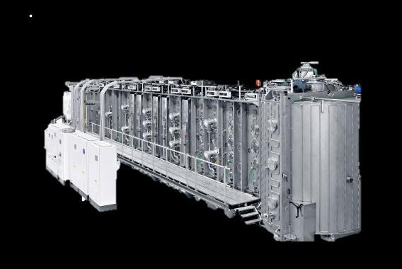
 killer")


12 Backplane Yield Challenge Example: Particles Smaller TFTs have more (& smaller) killer particles OLED TFT active area larger than LCD increasing chance of killer particle Increasing resolution increases # transistors/area requires smaller TFT increases # of killer particles 12

13 Semiconductor Methodologies for Advanced Displays Example: Yield Management You can t FIX What you can t SEE 13


")
14 Semiconductor Yield Management: Enabled by Inline SEM SEMI CD-SEM and SEM review introduction in 80s 10µm µm 1985 Display TODAY 0.18 µm µm 65 nm nm nm SEMI TODAY 90% processes are SEMed! Defect Inspection AOI (Sub 1um) Defect Review Inline SEM (with EDX) Defect Classification Yield management (connect the dots root cause) DISPLAY 14
 New way")


15 New Inspection Methodology for Advanced Displays Old way (Lab SEM) New way (Inline SEM) AOI Defects Map EBR in line Array Test Destructive Inspection Long Cycle Time Low Sampling Rate Non-destructive Inspection High Throughput High Sampling Rate 15
")
 Metrology Auto-CD")


16 Inline SEM Brings Semi Methodologies to Display Auto Process Inspection (API) Inspection & Review (defects) Auto Defect Review (ADR) Metrology Auto-CD (ACD) Process & Defects Composition Analysis LTPS Grain Analysis CD Measurements No Secco Etch ITO residue EDX & BSE ELA in-line Monitoring Accelerates yield by connecting the dots Inline SEM + yield management software fast ramp & high yield 16
17 YIELD YIELD w/ EBR PARTICLE DENSITY EBR Time Machine 3 Yield Entitlement 2 Yield Excursions 1 Ramp to Yield TIME System Fab-in Setup Pilot Pre -MP MP [ w/o EBR ] Process time 60sec Inspection 60 sec Measurement several mins Analysis several hours or days P I M Analysis [ w/ EBR ] Process time 60sec Inspection 60 sec Measurement several mins Analysis ~ several mins P I M Ana 17
 <1E-6g/m 2 day Long lifetime High deposition rate >2,500A/min High throughput Barrier Performance Stress Control Optical Transmittance Mask Depo Low stress ~ 0 Avoid cracking of metal")
18 Thin Film Encapsulation (TFE) Requirements Flexible OLED Device PROCESS REQUIREMENTS PURPOSE Depo temperature <100 Device protection Mask depo Mask deposition Bonding pad Water vapor transmission rate (WVTR) <1E-6g/m 2 day Long lifetime High deposition rate >2,500A/min High throughput Barrier Performance Stress Control Optical Transmittance Mask Depo Low stress ~ 0 Avoid cracking of metal electrodes or film itself High visible light transmittance >90% at wavelength 400nm Increase brightness Good adhesion No film peeling Device integrity High flexibility Mechanical duration Tolerate mechanical bending through lifetime Buffer Technology Conformal particle coverage No voids or diffusion channels Eliminate water and oxygen permeation 18

 KEY ADVANTAGES Superior WVTR & uniformity Particle control High system")
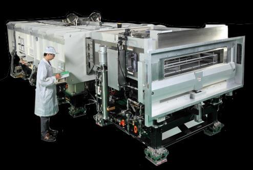
19 Enflexor Gen6H TFE Solutions for High Resolution Flexible OLED SUBSTRATE SIZE 925 x 1,500mm 2 SYSTEM ARCHITECTURE Single substrate operation system at cluster tool Max 5 TFE process chambers Mask chamber Pas chamber or DSSL (Dual Single Slot Load lock) Transfer chamber Dual arm vacuum robot TFE Process Chamber (max 5) Mask Chamber Transfer Chamber w/dual arm vacuum robot Pass Chamber or DSSL (Dual Single Slot Load lock) KEY ADVANTAGES Superior WVTR & uniformity Particle control High system reliability 19


20 One Cluster Solution Complete All TFE process in one cluster Vacuum Atm Vacuum Vacuum Connection to EV tool Flexible sequence control by MCC software High reliability mainframe and vacuum robot Mask deposition with auto mask exchange and mask stocker OLED EV Tool IN IJP OUT TFE Technology for OLED mass production new concept CVD Chamber Mask Stocker 2 nd Layer All process under vacuum pp-hmdso Upper-stream Load Lock Lower-stream Load Lock 3 Layer OLED EV Tool IN OUT Multiple Layer Stack 1 st Layer 3 rd Layer SiN CVD Chamber SiN 20

21 Displays are the window to the information universe and better displays are constantly in demand Many display technology inflections need materials engineering innovation Display industry can leverage semiconductor methodologies to enable increasingly complex displays 21
22
AMOLED Manufacturing Process Report SAMPLE
 AMOLED Manufacturing Process Report SAMPLE 2018 AMOLED Manufacturing Process Report The report analyzes the structure and manufacturing process by dividing AMOLED into small & medium-sized rigid OLED,
Advances in Roll-to-Roll Imprint Lithography for Display Applications Using Self Aligned Imprint Lithography. John G Maltabes HP Labs
 Advances in Roll-to-Roll Imprint Lithography for Display Applications Using Self Aligned Imprint Lithography John G Maltabes HP Labs Outline Introduction Roll to Roll Challenges and Benefits HP Labs Roll
Because Innovation Matters
 Because Innovation Matters Silicon Systems Group Toru Watanabe President, Applied Materials, Japan Semicon Japan November 30, 2010 Safe Harbor This presentation contains forward-looking statements, including
Flexible Electronics Production Deployment on FPD Standards: Plastic Displays & Integrated Circuits. Stanislav Loboda R&D engineer
 Flexible Electronics Production Deployment on FPD Standards: Plastic Displays & Integrated Circuits Stanislav Loboda R&D engineer The world-first small-volume contract manufacturing for plastic TFT-arrays
Display Technologies. Corning: The Technology Behind the Glass
 Display Technologies Corning: The Technology Behind the Glass Dr. David Chen Director, Application Engineering and Asia Commercial Technology Taiwan Corning Display Technologies Taiwan June 13, 2008 Forward
The Transition to Patterned Media in Hard Disk Drives
 The Transition to Patterned Media in Hard Disk Drives The Evolution of Jet and Flash Imprint Lithography for Patterned Media DISKCON San Jose Sept 24 rd, 2009 Paul Hofemann, Vice President, HDD Future
Scalable self-aligned active matrix IGZO TFT backplane technology and its use in flexible semi-transparent image sensors. Albert van Breemen
 Scalable self-aligned active matrix IGZO TFT backplane technology and its use in flexible semi-transparent image sensors Albert van Breemen Image sensors today 1 Dominated by silicon based technology on
PROCESS TECHNOLOGIES FOR ADVANCED ORGANIC ELECTRONIC DEVICES: MICRODISPLAYS, LIGHTING AND SOLAR CELLS
 PROCESS TECHNOLOGIES FOR ADVANCED ORGANIC ELECTRONIC DEVICES: MICRODISPLAYS, LIGHTING AND SOLAR CELLS Dr. Christian May Fraunhofer IPMS - Center for Organic Materials and Electronic Devices Dresden COMEDD
Phosphorescent OLED Technologies: The Next Wave. Plastic Electronics Conference Oct 9, 2012
 Phosphorescent OLED Technologies: The Next Wave Plastic Electronics Conference Oct 9, 2012 UDC Company Focus IP innovator, technology developer, patent licensor and materials supplier for the rapidly growing
projectors, head mounted displays in virtual or augmented reality use, electronic viewfinders
 Beatrice Beyer Figure 1. (OLED) microdisplay with a screen diagonal of 16 mm. Figure 2. CMOS cross section with OLED on top. Usually as small as fingernails, but of very high resolution Optical system
P I SCALE Creating an Open Access Flexible O L E D P ilo t L in e S e r vic e
 P I SCALE Creating an Open Access Flexible O L E D P ilo t L in e S e r vic e Pavel Kudlacek pavel.kudlacek@tno.nl P I - SCALE for 2017Flex 1 Lighting c h a lle n g e L ig h t in g c h a lle n g e At least
Industrial Inline Control for Advanced Vacuum Roll to Roll Systems. Gerhard Steiniger Web inspection - surface Quallity control 7.
 Industrial Inline Control for Advanced Vacuum Roll to Roll Systems Gerhard Steiniger Web inspection - surface Quallity control 7.4-7684 1 Industrial Inline Control for Advanced Vacuum Roll to Roll Systems
Applied Materials. 200mm Tools & Process Capabilities For Next Generation MEMS. Dr Michel (Mike) Rosa
 Rosa") Applied Materials 200mm Tools & Process Capabilities For Next Generation MEMS Dr Michel (Mike) Rosa 200mm MEMS Global Product / Marketing Manager, Components and Systems Group (CSG), Applied Global Services
Applied Materials 200mm Tools & Process Capabilities For Next Generation MEMS Dr Michel (Mike) Rosa 200mm MEMS Global Product / Marketing Manager, Components and Systems Group (CSG), Applied Global Services
Liquid Crystal Display (LCD)
") Liquid Crystal Display (LCD) When coming into contact with grooved surface in a fixed direction, liquid crystal molecules line up parallelly along the grooves. When coming into contact with grooved surface
Liquid Crystal Display (LCD) When coming into contact with grooved surface in a fixed direction, liquid crystal molecules line up parallelly along the grooves. When coming into contact with grooved surface
OLED Status quo and our position
 OLED Status quo and our position Information Day 2013 A Deep Dive into the LC&OLED Business Dr. Udo Heider Vice President OLED Darmstadt, Germany June 26, 2013 Disclaimer Remarks All comparative figures
MicroLED Displays: Global Trends & Opportunities for Equipment and Material Suppliers
 Picture: Sony From Technologies to Market MicroLED Displays: Global Trends & Opportunities for Equipment and Material Suppliers SEMICON EUROPA Jean-Christophe ELOY - CEO - Yole Développement 2017 AGENDA
UV Nanoimprint Tool and Process Technology. S.V. Sreenivasan December 13 th, 2007
 UV Nanoimprint Tool and Process Technology S.V. Sreenivasan December 13 th, 2007 Agenda Introduction Need tool and process technology that can address: Patterning and CD control Alignment and Overlay Defect
HB LEDs & OLEDs. Complete thin film process solutions
 HB LEDs & OLEDs Complete thin film process solutions Get off to a flying start for all your LED thin film deposition and etch processes From 2 inch to 8 inch Manual or fully automated substrate handling
Sep 09, APPLICATION NOTE 1193 Electronic Displays Comparison
 Sep 09, 2002 APPLICATION NOTE 1193 Electronic s Comparison Abstract: This note compares advantages and disadvantages of Cathode Ray Tubes, Electro-Luminescent, Flip- Dot, Incandescent Light Bulbs, Liquid
TipatOr. Liquid metal switch (LMS) display technology. Avi Fogel
 display technology. Avi Fogel") TipatOr Liquid metal switch (LMS) display technology Avi Fogel 972-52-5702938 avifog@gmail.com Who is behind TipatOr TipatOr emerged from a merger of 2 expert groups in the fields of MEMS and Displays
TipatOr Liquid metal switch (LMS) display technology Avi Fogel 972-52-5702938 avifog@gmail.com Who is behind TipatOr TipatOr emerged from a merger of 2 expert groups in the fields of MEMS and Displays
Flexible Flat Panel Display Technology
 1 Flexible Flat Panel Display Technology Gregory P. Crawford Division of Engineering, Brown University, Providence RI 1.1 Introduction The manufacturing of flat panel displays is a dynamic and continuously
[1.9] AMOLED 공정 Introduction OLED Materials Patterning Process Process Equipments
![[1.9] AMOLED 공정 Introduction OLED Materials Patterning Process Process Equipments](/thumbs/73/69073032.jpg "[1.9] AMOLED 공정 Introduction OLED Materials Patterning Process Process Equipments") [1.9] AMOLED 공정 1.9.1. Introduction 1.9.2. OLED Materials 1.9.3. Patterning Process 1.9.4. Process Equipments OLED : Organic Light Emitting Diode Organic EL : Organic Electroluminescent 재료및공정 재료의발광메카니즘
[1.9] AMOLED 공정 1.9.1. Introduction 1.9.2. OLED Materials 1.9.3. Patterning Process 1.9.4. Process Equipments OLED : Organic Light Emitting Diode Organic EL : Organic Electroluminescent 재료및공정 재료의발광메카니즘
OLED ON CMOS: WHAT ABOUT THINNING AND BENDING?
 Large cost-effective OLED microdisplays and their applications OLED ON CMOS: WHAT ABOUT THINNING AND BENDING? IDW2017 tony.maindron@cea.fr T. Maindron, B. Chambion, A. Vandeneynde, S. Gétin, M. Provost,
Leveraging 300 mm Technology Solutions to Enable New MEMS Process Capabilities
 Leveraging 300 mm Technology Solutions to Enable New MEMS Process Capabilities Evan Patton Semicon Europa November 2017 Lam Research Corp. 1 Presentation Outline The Internet of Things (IoT) as a market
Automation in Semiconductor Manufacturing IEDM, San Francisco, 1982 Keynote Speech
 Automation in Semiconductor Manufacturing IEDM, San Francisco, 1982 Keynote Speech Commentary Alongside ISSCC, IEDM is the most traditional academic conference in the semiconductor field, and it is held
Thin-Film Encapsulation of Organic Light Emitting Devices (OLEDs) Dr. Emilie Galand Huntsman Advanced Materials CSEM Plastic Optoelectronics - Basel
 Dr. Emilie Galand Huntsman Advanced Materials CSEM Plastic Optoelectronics - Basel") Thin-Film Encapsulation of Organic Light Emitting Devices (OLEDs) Dr. Emilie Galand CSEM Plastic Optoelectronics - Basel 25th June 2010 About Huntsman Huntsman is a global manufacturer and marketer of
Thin-Film Encapsulation of Organic Light Emitting Devices (OLEDs) Dr. Emilie Galand CSEM Plastic Optoelectronics - Basel 25th June 2010 About Huntsman Huntsman is a global manufacturer and marketer of
Joint Development of Ultra-Bright, Inorganic EL Light-Emitting Materials. November 2, 2005 KURARAY CO., LTD.
 Joint Development of Ultra-Bright, Inorganic EL Light-Emitting Materials November 2, 2005 KURARAY CO., LTD. Sales Trends of Display-related Products (Kuraray (standalone)) FY1994 FY1999 FY2004 Sales Ratio
AIXTRON in EXCILIGHT project
 AIXTRON SE AIXTRON in EXCILIGHT project Gintautas Simkus ABOUT AIXTRON 2 Who we are Headquarter based in Herzogenrath, Germany Worldwide presence with 14 sales/representatives offices and production facilities
:: Reduce needs for heat dissipation components. :: Extend battery life in mobile products. :: Save power and reduce heat generation in TVs
 UniversalPHOLED Technology and Materials UniversalPHOLED Phosphorescent OLED technology and materials offer record-breaking performance to bring competitive advantages to your OLED display and lighting
Development of OLED Lighting Applications Using Phosphorescent Emission System
 Development of OLED Lighting Applications Using Phosphorescent Emission System Kazuhiro Oikawa R&D Department OLED Lighting Business Center KONICA MINOLTA ADVANCED LAYERS, INC. October 10, 2012 Outline
1. Publishable summary
 1. Publishable summary 1.1. Project objectives. The target of the project is to develop a highly reliable high brightness conformable low cost scalable display for demanding applications such as their
Characteristics of the liquid crystals market
 Characteristics of the liquid crystals market Information Day 2013 A Deep Dive into the LC&OLED Business Walter Galinat President of Performance Materials Darmstadt, Germany June 26, 2013 Disclaimer Remarks
Semiconductors Displays Semiconductor Manufacturing and Inspection Equipment Scientific Instruments
 Semiconductors Displays Semiconductor Manufacturing and Inspection Equipment Scientific Instruments Electronics 110-nm CMOS ASIC HDL4P Series with High-speed I/O Interfaces Hitachi has released the high-performance
Display Technologies CMSC 435. Slides based on Dr. Luebke s slides
 Display Technologies CMSC 435 Slides based on Dr. Luebke s slides Recap: Transforms Basic 2D Transforms: Scaling, Shearing, Rotation, Reflection, Composition of 2D Transforms Basic 3D Transforms: Rotation,
Wafer Thinning and Thru-Silicon Vias
 Wafer Thinning and Thru-Silicon Vias The Path to Wafer Level Packaging jreche@trusi.com Summary A new dry etching technology Atmospheric Downstream Plasma (ADP) Etch Applications to Packaging Wafer Thinning
FLEX2017 June, Monterey, USA Dr Mike Cowin, CMO, SmartKem.
 FLEX2017 June, Monterey, USA Dr Mike Cowin, CMO, SmartKem. FLEX2017 June, Monterey, USA Dr Mike Cowin, CMO, SmartKem. EU H2020 FLEXTRANs Grant Objectives A 24 month project (started September 2016) (Grant
Solid State Devices 4B6
 Solid State Devices 4B6 Lecture 13 Projection and 3D displays: LCD, DLP and LCOS Daping Chu Lent 2016 Development of flat panel displays (FPDs) (LCD) in early days 1 A 105 inch TFT-LCD 4k2k curved panel
Abstract. Keywords INTRODUCTION. Electron beam has been increasingly used for defect inspection in IC chip
 Abstract Based on failure analysis data the estimated failure mechanism in capacitor like device structures was simulated on wafer in Front End of Line. In the study the optimal process step for electron
Display Systems. Viewing Images Rochester Institute of Technology
 Display Systems Viewing Images 1999 Rochester Institute of Technology In This Section... We will explore how display systems work. Cathode Ray Tube Television Computer Monitor Flat Panel Display Liquid
ABSTRACT. Keywords: 3D NAND, FLASH memory, Channel hole, Yield enhancement, Defect inspection, Defect reduction DISCUSSION
 Yield enhancement of 3D flash devices through broadband brightfield inspection of the channel hole process module Jung-Youl Lee a, Il-Seok Seo a, Seong-Min Ma a, Hyeon-Soo Kim a, Jin-Woong Kim a DoOh Kim
R2R Processing of Flexible Devices
 R2R Processing of Flexible Devices Mani Thothadri, PhD Senior Director, New Business & Strategic Initiatives Display & Flexible Technologies Group Flextech June 20, 2017 Acknowledgements Dan Forster Christoph
SNU PRECISION CO., LTD
 SNU PRECISION CO., LTD 1629-2 Nakseongdae-dong, Kwanak-ku in Seoul, SOUTH KOREA The First Quarter 2011 Disclaimer This document has been prepared by SNU Precision CO., Ltd.( the Company ). Until 2010,
EQUIPMENT VACUUM WEB COATING SYSTEMS ROLL-TO-ROLL ROLL-TO-ROLL
 ROLL-TO-ROLL EQUIPMENT VACUUM WEB COATING SYSTEMS ROLL-TO-ROLL VACUUM WEB COATING APPLICATIONS VON ARDENNE provides tailored web coating solutions for today s most ambitious thin-film applications on polymer
Defect Analysis of Roll-to-Roll SAIL Manufactured Flexible Display Backplanes
 Defect Analysis of Roll-to-Roll SAIL Manufactured Flexible Display Backplanes Carl Taussig, Richard E. Elder, Warren B. Jackson, Albert Jeans, Mehrban Jam, Ed Holland, Hao Luo, John Maltabes, Craig Perlov,
 Chapter 1 Introduction --------------------------------------------------------------------------------------------------------------- 1.1 Overview of the Organic Light Emitting Diode (OLED) Displays Flat
PLASMA DISPLAY PANEL (PDP) DAEWOO D I G I T A L DIGITAL TV DEVISION
 DAEWOO D I G I T A L DIGITAL TV DEVISION") PLASMA DISPLAY PANEL (PDP) DAEWOO D I G I T A L 2002. 5 DAEWOO ELECTRONICS CO., LTD DIGITAL TV DEVISION WHAT IS PLASMA DISPLAY PANEL? 1. PDP refers to plasma display panel. It was named as PDP by the faculty
PLASMA DISPLAY PANEL (PDP) DAEWOO D I G I T A L 2002. 5 DAEWOO ELECTRONICS CO., LTD DIGITAL TV DEVISION WHAT IS PLASMA DISPLAY PANEL? 1. PDP refers to plasma display panel. It was named as PDP by the faculty
ADDING AN O TO LEDS STATUS AND PERSPECTIVES OF ORGANIC LIGHT EMITTING DIODES PAWEL E. MALINOWSKI, TUNGHUEI KE LED EVENT 2017
 ADDING AN O TO LEDS STATUS AND PERSPECTIVES OF ORGANIC LIGHT EMITTING DIODES PAWEL E. MALINOWSKI, TUNGHUEI KE LIVING ROOM NOT SO LONG AGO... 2 Source: Warner Bros. Incadescent CRT 3 Source: Warner Bros.
FASwitch - A MEMS Display Backplane Manufactured by Flex Circuit Methods
 FASwitch - A MEMS Display Backplane Manufactured by Flex Circuit Methods Presenter: Dr. Nicholas F. Pasch Rolltronics Corporation 750 Menlo Ave. Menlo Park, CA 94025 npasch@rolltronics.com Introduction
Flat Panel Displays: 1. Introduction
 OSE-6820 Flat Panel Displays: 1. Introduction Prof. Shin-Tson Wu College of Optics & Photonics University of Central Florida Email: swu@mail.ucf.edu Office: CREOL 280 Phone: 407-823-4763 UCF College of
THE challenges facing today s mobile
 MEMS displays MEMS-Based Display Technology Drives Next-Generation FPDs for Mobile Applications Today, manufacturers of mobile electronic devices are faced with a number of competitive challenges. To remain
Screens; media that use additive primaries
 Image display Display is the final stage in the image processing pipeline: Continuous scenes are acquired and digitally processed. The display process essentially converts the discrete image back to continuous
Pressure sensor. Surface Micromachining. Residual stress gradients. Class of clean rooms. Clean Room. Surface micromachining
 Pressure sensor Surface Micromachining Deposit sacrificial layer Si PSG By HF Poly by XeF2 Pattern anchors Deposit/pattern structural layer Etch sacrificial layer Surface micromachining Structure sacrificial
Overcoming Challenges in 3D NAND Volume Manufacturing
 Overcoming Challenges in 3D NAND Volume Manufacturing Thorsten Lill Vice President, Etch Emerging Technologies and Systems Flash Memory Summit 2017, Santa Clara 2017 Lam Research Corp. Flash Memory Summit
Development of OLED Lighting Panel with World-class Practical Performance
 72 Development of OLED Lighting Panel with World-class Practical Performance TAKAMURA MAKOTO *1 TANAKA JUNICHI *2 MORIMOTO MITSURU *2 MORI KOICHI *3 HORI KEIICHI *4 MUSHA MASANORI *5 Using its proprietary
Light, Bright, and. Julie Brown Universal Display Corporation.
 Light, Bright, and Julie Brown Universal Display Corporation jjbrown@universaldisplay.com May 3, 2006 A Perspective OLEDs Yesterday OLEDs Today OLEDs Tomorrow Milestones in OLEDs (1960-2000) 1963 Pope
Self-Aligned Double Patterning for 3xnm Flash Production
 Self-Aligned Double Patterning for 3xnm Flash Production Chris Ngai Dir of Process Engineering & Lithography Maydan Technology Center Group Applied Materials, Inc. July 16 th, 2008 Overview Double Patterning
VACUUM WEB COATING SYSTEMS ROLL-TO-ROLL ROLL-TO-ROLL VACUUM WEB COATING SYSTEMS
 VACUUM WEB COATING SYSTEMS ROLL-TO-ROLL ROLL-TO-ROLL VACUUM WEB COATING SYSTEMS VACUUM WEB COATING APPLICATIONS VON ARDENNE provides tailored web coating solutions for today s most ambitious thin-film
Application note. Materials. Introduction. Authors. Travis Burt, Huang ChuanXu*, Andy Jiang* Agilent Technologies Mulgrave, Victoria, Australia
 Performance of compact visual displays measuring angular reflectance of optically active materials using the Agilent Cary 7000 Universal Measurement Spectrophotometer (UMS) Application note Materials Authors
Next Generation of Poly-Si TFT Technology: Material Improvements and Novel Device Architectures for System-On-Panel (SOP)
") Next Generation of Poly-Si TFT Technology: Material Improvements and Novel Device Architectures for System-On-Panel (SOP) Tolis Voutsas* Paul Schuele* Bert Crowder* Pooran Joshi* Robert Sposili* Hidayat
Next Generation of Poly-Si TFT Technology: Material Improvements and Novel Device Architectures for System-On-Panel (SOP) Tolis Voutsas* Paul Schuele* Bert Crowder* Pooran Joshi* Robert Sposili* Hidayat
The Technological Trends of Future AMOLED
 Invited Paper The Technological Trends of Future AMOLED Jong hyuk Lee*, Hye Dong Kim, Chang Ho Lee, Hyun-Joong Chung, Sung Chul Kim, and Sang Soo Kim Technology Center, Samsung Mobile Display Co., LTD
High-resolution screens have become a mainstay on modern smartphones. Initial. Displays 3.1 LCD
 3 Displays Figure 3.1. The University of Texas at Austin s Stallion Tiled Display, made up of 75 Dell 3007WPF LCDs with a total resolution of 307 megapixels (38400 8000 pixels) High-resolution screens
Flat Panel Displays: LCD Technologies and Trends
 Flat Panel Displays: LCD Technologies and Trends Robert Dunhouse, Sr. Engineering Manager, Display BU Class ID: 4C01B Renesas Electronics America Inc. Robert F. Dunhouse, Jr. Sr. Engineering Manager, Display
Technology White Paper Plasma Displays. NEC Technologies Visual Systems Division
 Technology White Paper Plasma Displays NEC Technologies Visual Systems Division May 1998 1 What is a Color Plasma Display Panel? The term Plasma refers to a flat panel display technology that utilizes
The Company. A leading OLED player
 The Company A leading OLED player Novaled is the company to trade with, work for and invest in. Our company focuses on proprietary organic materials and complementary innovative technologies for superior
DARPATech 99 DARPA/MTO. Bruce Gnade
 DARPATech 99 DARPA/MTO Bruce Gnade High Definition Systems Objective: Develop leading-edge display technology to meet diverse, but specific, DoD needs. The goals include increased power efficiency, reduced
The Flat Panel Display Paradigm: Successful Implementation of Microelectronic Processes on Gigantic Wafers
 The Flat Panel Display Paradigm: Successful Implementation of Microelectronic Processes on Gigantic Wafers Dr. Zvi Yaniv Applied Nanotech, Inc. 3006 Longhorn Blvd., Suite 107 Austin, TX 78758 Phone 512-339-5020
Organic light emitting diode (OLED) displays
 displays") Ultra-Short Pulse Lasers Enable Precision Flexible OLED Cutting FLORENT THIBAULT, PRODUCT LINE MANAGER, HATIM HALOUI, APPLICATION MANAGER, JORIS VAN NUNEN, PRODUCT MARKETING MANAGER, INDUSTRIAL PICOSECOND
Ultra-Short Pulse Lasers Enable Precision Flexible OLED Cutting FLORENT THIBAULT, PRODUCT LINE MANAGER, HATIM HALOUI, APPLICATION MANAGER, JORIS VAN NUNEN, PRODUCT MARKETING MANAGER, INDUSTRIAL PICOSECOND
Displays and framebuffers
 Reading Optional Displays and framebuffers Brian Curless CSE 557 Autumn 2017 OpenGL Programming Guide (the red book available online): First four sections of chapter 2 First section of chapter 6 Foley
ORGANIC ELECTRONICS PROCESS DEVELOPMENT AND ENCAPSULATION TECHNOLOGIES
 FRAUNHOFER INSTITUTE FOR ORGANIC ELECTRONICS, ELECTRON BEAM AND PLASMA TECHNOLOGY FEP ORGANIC ELECTRONICS PROCESS DEVELOPMENT AND ENCAPSULATION TECHNOLOGIES 2 PROFILE Fraunhofer FEP combines research and
 Chapter 3 Evaluated Results of Conventional Pixel Circuit, Other Compensation Circuits and Proposed Pixel Circuits for Active Matrix Organic Light Emitting Diodes (AMOLEDs) -------------------------------------------------------------------------------------------------------
Manufacturing Cost Analysis by Display Technology
 Manufacturing Cost Analysis by Display Technology Jimmy Kim, Ph.D. Principal Analyst / IHS Markit Technology November 2 nd, 2016 2 LCD, OLED and Flexible Mobile Display 3 OLED trying to catch up LCD for
VARIOUS DISPLAY TECHNOLOGIESS
 VARIOUS DISPLAY TECHNOLOGIESS Mr. Virat C. Gandhi 1 1 Computer Department, C. U. Shah Technical Institute of Diploma Studies Abstract A lot has been invented from the past till now in regards with the
2006 Taiwan FPD International Conference May 25-26, 2006 Taipei International Convention Center Brightness Enhancement Films
 1 2006 Taiwan FPD International Conference May 25-26, 2006 Taipei International Convention Center Brightness Enhancement Films Bill Smyth Senior Manager, Marketing & Business Development 3M Optical Systems
PUBLISHABLE Summary To provide OLED stacks with improved reliability Provide improved thin film encapsulation
 PUBLISHABLE Summary SCOOP is a European funded project (FP7 project number 287595 SCOOP). It is focused on OLED technology, microdisplays based on the combination of OLED with CMOS technology, and innovative
Zeon PDF Driver Trial
 OLED Technology and Product Development in RiTdisplay Chorng-Shyr Jou RiTdisplay csjou@ritdisplay.com 1 Contents I. The Technologies & Challenge of OLED II. The Application of OLED III.Who are Working
Screen investigations for low energetic electron beams at PITZ
 1 Screen investigations for low energetic electron beams at PITZ S. Rimjaem, J. Bähr, H.J. Grabosch, M. Groß Contents Review of PITZ setup Screens and beam profile monitors at PITZ Test results Summary
Press Release Plastic Electronics 2013 October 8th 10th, 2013, in Dresden/Germany Hall 2, booth no. 292 (joint booth of Organic Electronic Saxony)
") Press Release Plastic Electronics 2013 October 8th 10th, 2013, in Dresden/Germany Hall 2, booth no. 292 (joint booth of Organic Electronic Saxony) Flexible OLED from the roll Tridonic Dresden and Fraunhofer
Press Release Plastic Electronics 2013 October 8th 10th, 2013, in Dresden/Germany Hall 2, booth no. 292 (joint booth of Organic Electronic Saxony) Flexible OLED from the roll Tridonic Dresden and Fraunhofer
OLED Technology Introduction
 OLED Technology Introduction An organic light emitting diode (OLED) consists of several semiconducting organic layers sandwiched between two electrodes at least one of them being transparent. A simplified
Introduction to OLED lighting and key challenges for the industry
 Introduction to OLED lighting and key challenges for the industry Dr. Wolfgang Doetter Authorized Company Officer OLEDWorks Global Q-EHS Manager & Senior Integral Project Manager 1 OLEDs A new perception
Requirement for graphic arts display
 Requirement for graphic arts display Content Development Division of National Digital Archives Program, Taiwan Date: 95/12/5 中島賢人 : Masato Nakashima Product Manager, Graphic Solutions Overseas Sales &
Monitor and Display Adapters UNIT 4
 Monitor and Display Adapters UNIT 4 TOPIC TO BE COVERED: 4.1: video Basics(CRT Parameters) 4.2: VGA monitors 4.3: Digital Display Technology- Thin Film Displays, Liquid Crystal Displays, Plasma Displays
SUPPLEMENTARY INFORMATION
 User-interactive electronic-skin for instantaneous pressure visualization Chuan Wang 1,2,3, David Hwang 1,2,3, Zhibin Yu 1,2,3, Kuniharu Takei 1,2,3, Junwoo Park 4, Teresa Chen 4, Biwu Ma 3,4, and Ali
Overview of All Pixel Circuits for Active Matrix Organic Light Emitting Diode (AMOLED)
") Chapter 2 Overview of All Pixel Circuits for Active Matrix Organic Light Emitting Diode (AMOLED) ---------------------------------------------------------------------------------------------------------------
Chapter 2 Overview of All Pixel Circuits for Active Matrix Organic Light Emitting Diode (AMOLED) ---------------------------------------------------------------------------------------------------------------
1 Your computer screen
 U.S.T.H.B / C.E.I.L Unit 7 Computer science L2 (S2) 1 Your computer screen Discuss the following questions. 1 What type of display do you have? 2 What size is the screen? 3 Can you watch TV on your PC
New Worlds for Polymers: Organic Transistors, Light Emitting Diodes, and Optical Waveguides Ed Chandross
 New Worlds for Polymers: Organic Transistors, Light Emitting Diodes, and Optical Waveguides Ed Chandross Materials Chemistry, LLC 1 Polymers in the Electronic Industry Enabling Materials Active Materials?
Nano-Imprint Lithography Infrastructure: Imprint Templates
 Nano-Imprint Lithography Infrastructure: Imprint Templates John Maltabes Photronics, Inc Austin, TX 1 Questions to keep in mind Imprint template manufacturability Resolution Can you get sub30nm images?
Present status of Roll-to-Roll Fabrication for OLED lighting
 Present status of Roll-to-Roll Fabrication for OLED lighting Michael Stanel, Tomasz Wański, Stefan Mogck Fraunhofer Institute for Organic Electronics, Electron Beam and Plasma Technology FEP AIMCAL, Web
 Page 1 of 8 Main > Electronics > Computers How OLEDs Work by Craig Freudenrich, Ph.D. Introduction to How OLEDs Work Imagine having a high-definition TV that is 80 inches wide and less than a quarter-inch
An Overview of OLED Display Technology
 page:1 An Overview of OLED Display Technology Homer Antoniadis OSRAM Opto Semiconductors Inc. San Jose, CA page:2 Outline! OLED device structure and operation! OLED materials (polymers and small molecules)!
Parts of dicing machines for scribing or scoring semiconductor wafers , , , , ,
 US-Rev3 26 March 1997 With respect to any product described in or for Attachment B to the Annex to the Ministerial Declaration on Trade in Information Technology Products (WT/MIN(96)/16), to the extent
Forward-Looking Statements
 Forward-Looking Statements Information in this presentation regarding MagnaChip s forecasts, business outlook, expectations and beliefs are forward-looking statements within the meaning of the Private
Present and future of OLED lighting
 Present and future of OLED lighting Dr. Wolfgang Dötter Authorized Company Officer OLEDWorks Global Q-EHS Manager & Senior Integral Project Manager 1 Vision In 10 years there will be only Solid State Lighting;
1. Introduction. 1.1 Graphics Areas. Modeling: building specification of shape and appearance properties that can be stored in computer
 1. Introduction 1.1 Graphics Areas Modeling: building specification of shape and appearance properties that can be stored in computer Rendering: creation of shaded images from 3D computer models 2 Animation:
Results of recent photocathode studies at FLASH. S. Lederer, S. Schreiber DESY. L. Monaco, D. Sertore, P. Michelato INFN Milano LASA
 Results of recent photocathode studies at FLASH S. Lederer, S. Schreiber DESY L. Monaco, D. Sertore, P. Michelato INFN Milano LASA FLASH seminar October 21 st, 2008 Outlook Cs 2 Te photocathodes cw QE
Taking Technology to the Marketplace. Aram Mooradian Founder & CTO Sunnyvale, CA, USA
 Taking Technology to the Marketplace Aram Mooradian Founder & CTO Sunnyvale, CA, USA aram@novalux.com Requirements Market Technology Product Price Timing Good Investors Good People Path to Success Absolutely
Solution Processable OLEDs. Anna Hayer EuroDisplay /09/2013
 Solution Processable LEDs Merck KGaA Anna Hayer EuroDisplay 2013 Content 1 Introduction 2 LED Basics 3 Challenges for Solution Processing 4 Current Results 5 Summary 2 EuroDisplay 2013 Hayer - Merck Solution
This talk covers currently available display technology.
 Introduction to Current Display Technologies for Medical Image Viewing Perspectives for the TG270 Update on Display Quality Control Alisa Walz-Flannigan, PhD (DABR) Mayo Clinic, Rochester, Minnesota AAPM
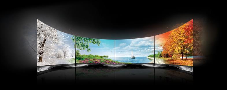
Deep Dive into Curved Displays
 Deep Dive into Curved Displays First introduced at CES 2013, curved displays were primarily used for TVs. Today s curved technology employs a range of backlighting technologies, comes in a variety of sizes,
Basically we are fooling our brains into seeing still images at a fast enough rate so that we think its a moving image.
 Basically we are fooling our brains into seeing still images at a fast enough rate so that we think its a moving image. The formal definition of a Moving Picture... A sequence of consecutive photographic