InvenSense Fabless Model for the MEMS Industry
|
|
|
- Adrian Hall
- 6 years ago
- Views:
Transcription


1 InvenSense Fabless Model for the MEMS Industry HKSTP Symposium Aug 2016 InvenSense, Inc. Proprietary
2 Outline MEMS Market InvenSense CMOS-MEMS Integration InvenSense Shuttle Program and Process
3 MEMS MARKET
4 US$M MEMS Markets by Applications $18,000 $16,000 $14,000 $12,000 $10,000 $8,000 $6,000 $4,000 $2,000 Automotive Consumer Industrial Telecom $ Yole Devéloppement Status of the MEMS Industry April 2014
5 US$M MEMS for Internet of Things (IoT) Market $1,200 $1,000 $800 $600 $400 $200 $ Yole Devélopement Status of the MEMS Industry April 2014


6 Ambient Computing Internet of Things AlwaysOn, and Intuitively Interactive Apps and Services Location + Activity + Time + Environment Sensor Sensor wearabl e energy security control sports 15
7 INVENSENSE


 11.16.")

8 ($ in Millions) $372 $253 $209 $153 $80 $97 $3 $8 $29 FY2007 FY2008 FY2009 FY2010 FY2011 FY 2012 FY2013 FY2014 FY2015 Founded 2003 Headquarters San Jose, CA Cash Position $242M (As of 28 June 2015) NYSE: INVN Employees 665 Note: Company fiscal year ends Sunday closest to March 31.


9 Calgary, Canada San Jose, Calif Boston, Mass Grenoble, France Bratislava, Slovakia Milan, Italy Seoul, Korea Shenzhen, China Yokohama, Japan Shanghai, China Hsinchu, Taiwan 9


10 Select Customers Imaging 12% Other/ IoT 10% FY15 Mobile 78% 10


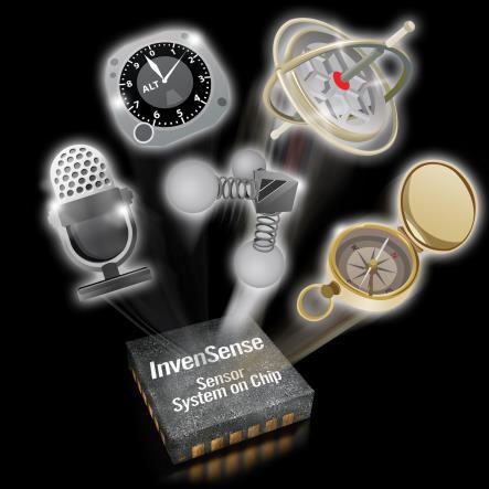


11 Unique Technology & Intellectual Property MEMS Microphones MEMS Sensors Sensor Fusion Fabrication Stabilization Navigation Fingerprint Authentication 11


12 Fabless Business Model CMOS-MEMS Wafer Sort Packaging Proprietary Testing TSMC GlobalFoundries InvenSense ASE Amkor Lingsen InvenSense 1 Billion Unit Capacity Super Efficient Supply Chain Easy Fulfillment of Short Lead Time Upsides 12
13 VALUE OF WAFER-LEVEL CMOS-MEMS INTEGRATION


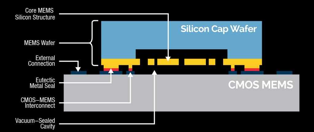
14 Wafer-level Integration Advantages Low Parasitics Minimize routing and external interconnect Wafer Level Sealing / Packaging Wafer Level Testing Designed for Test

")


15 Semiconductor Manufacturing Flow for MEMS InvenSense Process CMOS MEMS Wafer TSMC Wafer Sort (e-test) Singulation Integrated Chip Assembly 1 chip Final Test 15 CMOS-MEMS Wafer Sort Packaging FT & Ship Traditional MEMS Process CMOS Wafer Foundry 1 MEMS Wafer Foundry 2 WAT CMOS only MEMS WAT Singulation ASIC Chip Singulation MEMS Chip Assembly Multi-Chip Final Test
16 Applications Benefiting from CMOS Integration High Sensitivity Low signal and low noise requirement High Complexity Large arrays and closed-loop control High Integration Sensor fusion and high-density SoC Low Cost and Small Size Mobile devices and Internet of Things Implantable Sensors
17 INVENSENSE SHUTTLE
18 Challenges for MEMS Product Development Fabrication One product - one process increases barrier to entry Find foundry able and willing to bring up new process Development Fighting both design and process simultaneously Need for fast design iterations to keep up with market New start ups need $50M-$70M, 7+ years to profit Production Over 50% of costs are in package and test Establish high yield and quality Establish reliable supply chain to deliver high quality at low cost Growth Extend and expand product base Maintain competitiveness - add more value and lower cost
19 InvenSense Shuttle Objectives Offer a proven and high volume CMOS-MEMS platform for MEMS fabrication Speed up development cycle and time to commercialization Bring the fabless CMOS scalable production model to MEMS industry
20 InvenSense Shuttle Payoff Innovators Faster development cycle by focusing on innovative MEMS designs and not fabrication Faster and lower cost development cycles InvenSense Collaborate on new ideas and opportunities Building a closer relationship with innovators Potential royalty revenue Market More innovations in MEMS More standardization in the industry


 AlN + Si MEMS 18um CMOS")
21 InvenSense Shuttle Processes Standard (SOI) Shuttle Process used on InvenSense inertial sensors SOI MEMS integrated with 0.18um CMOS Suitable for: Inertial, Resonators, Pressure, RF Piezo Shuttle Extension of standard process to piezo (AlN) AlN + Si MEMS integrated with 0.18um CMOS Suitable for: RF, Ultrasound, IR, Timing, Audio
 6 Metal layers MEMS Anchored to handle only MEMS Anchored to handle and CMOS Upper Cavity CMOS Contact Moveable MEMS Wire-Bond Pad Bottom Cavity in CMOS")
22 SOI Shuttle Process Overview MEMS Single-Crystal Si MEMS Structural layer DRIE structure definition No release etch requirement Aluminum-Germanium wafer bond CMOS 0.18 mm Process High voltage LDMOS (up to 24v) 6 Metal layers MEMS Anchored to handle only MEMS Anchored to handle and CMOS Upper Cavity CMOS Contact Moveable MEMS Wire-Bond Pad Bottom Cavity in CMOS Electrode to interact with MEMS Eutectic Bond CMOS Wafer CMOS Top Metal Device Layer Handle Wafer IMD+Pass. Germanium Buried Oxide Top Aluminum
23 Piezo Shuttle Process Overview MEMS AlN + Silicon structural layer Top and Bottom piezo electrodes Port opening to expose MEMS to environment TCF compensation options Aluminum-Germanium wafer bond CMOS 0.18 mm Process High voltage LDMOS (up to 24v) 6 Metal layers MEMS wafer Oxide Al Device layer CMOS wafer AlN Mo Ge IMD


24 Standard Shuttle Process Flow

25 Piezo Shuttle Process Flow MEMS wafer Oxide Al Device layer CMOS wafer AlN Mo Ge IMD 25
26 SAMPLE SHUTTLE PROJECTS


27 Project: Mode-Reversal FM Gyro Collaborators: D. Horsley, B. Boser UC Davis/Berkeley Process: SOI 27


28 Project: CMOS-Integrated High- Frequency Resonators Collaborators: T. Kenny, B. Murmann Stanford University Process: SOI 28


29 Project: Nano-Power Pressure Sensor Collaborators: S. Gambini University of Melbourne Process: SOI 29
30 Shuttle Projects: IR Sensor Collaborators: Mina Rais-Zadeh University of Michigan Process: Piezo IR on IR off 30

 mv 25 2 1 20 0-1 -2-3 -4-5 -4-3 -2-1 0 1 2")
31 Projects: Ultrasonic Fingerprint Sensor Lateral distance - y (mm) Collaborators: D. Horsley, B. Boser UC Davis/Berkeley Process: Piezo Fingerprint (optic) 4 3 Fingerprint (ultrasonic) mv Lateral distance - x (mm)
32 INVENSENSE SHUTTLE PROGRAM

33 Summary InvenSense Shuttle Brings the CMOS fabless model to MEMS industry Increases MEMS Value through system integration Enables revolutionary new Smart MEMS products Opens world class foundries to MEMS innovators Reduces time to market Next Shuttle tapes out in December 2016 For More Information Contact us: Register on NF Shuttle Web Site:
34 Thank You InvenSense InvenSense, Inc. Company Inc. Proprietary Confidential
Advanced WLP Platform for High-Performance MEMS. Presented by Dean Spicer, Director of Engineering
 Advanced WLP Platform for High-Performance MEMS Presented by Dean Spicer, Director of Engineering 1 May 11 th, 2016 1 Outline 1. Application Drivers for High Performance MEMS Sensors 2. Approaches to Achieving
Applied Materials. 200mm Tools & Process Capabilities For Next Generation MEMS. Dr Michel (Mike) Rosa
 Rosa") Applied Materials 200mm Tools & Process Capabilities For Next Generation MEMS Dr Michel (Mike) Rosa 200mm MEMS Global Product / Marketing Manager, Components and Systems Group (CSG), Applied Global Services
Applied Materials 200mm Tools & Process Capabilities For Next Generation MEMS Dr Michel (Mike) Rosa 200mm MEMS Global Product / Marketing Manager, Components and Systems Group (CSG), Applied Global Services
Next Generation MEMS Manufacturing The ConFab Alissa M. Fitzgerald, Ph.D., Founder & Managing Member
 Next Generation MEMS Manufacturing The ConFab 2017 Alissa M. Fitzgerald, Ph.D., Founder & Managing Member Overview About AMFitzgerald Retrospective: MEMS technology history and markets Next generation
2016, Amkor Technology, Inc.
 1 Standardization of Packaging for the Internet of Things Adrian Arcedera l VP of MEMS and Sensor Products 2 About Amkor Technology Amkor Technology, Inc. is one of the world's largest and most accomplished
2016, Amkor Technology, Inc.
 1 Standardization of Packaging for the Internet of Things Adrian Arcedera l VP of MEMS and Sensor Products 2 About Amkor Technology Amkor Technology, Inc. is one of the world's largest and most accomplished
Vesper VM1000 Piezoelectric MEMS Microphone
 Vesper VM1000 Piezoelectric MEMS Microphone MEMS report by Sylvain Hallereau February 2017 21 rue la Noue Bras de Fer 44200 NANTES - FRANCE +33 2 40 18 09 16 info@systemplus.fr www.systemplus.fr 2017 System
9 rue Alfred Kastler - BP Nantes Cedex 3 - France Phone : +33 (0) website :
 website :") 9 rue Alfred Kastler - BP 10748-44307 Nantes Cedex 3 - France Phone : +33 (0) 240 180 916 - email : info@systemplus.fr - website : www.systemplus.fr January 2012 Written by: Maher SAHMIMI DISCLAIMER :
9 rue Alfred Kastler - BP 10748-44307 Nantes Cedex 3 - France Phone : +33 (0) 240 180 916 - email : info@systemplus.fr - website : www.systemplus.fr January 2012 Written by: Maher SAHMIMI DISCLAIMER :
Wafer Thinning and Thru-Silicon Vias
 Wafer Thinning and Thru-Silicon Vias The Path to Wafer Level Packaging jreche@trusi.com Summary A new dry etching technology Atmospheric Downstream Plasma (ADP) Etch Applications to Packaging Wafer Thinning
STMicroelectronics L2G2IS 2-Axis Gyroscope for OIS
 STMicroelectronics L2G2IS 2-Axis Gyroscope for OIS MEMS report by Romain Fraux October 2016 21 rue la Noue Bras de Fer 44200 NANTES - FRANCE +33 2 40 18 09 16 info@systemplus.fr www.systemplus.fr 2016
9 rue Alfred Kastler - BP Nantes Cedex 3 - France Phone : +33 (0) website :
 website :") 9 rue Alfred Kastler - BP 10748-44307 Nantes Cedex 3 - France Phone : +33 (0) 240 180 916 - email : info@systemplus.fr - website : www.systemplus.fr March 2011 - Version 1 Written by: Romain FRAUX DISCLAIMER
9 rue Alfred Kastler - BP 10748-44307 Nantes Cedex 3 - France Phone : +33 (0) 240 180 916 - email : info@systemplus.fr - website : www.systemplus.fr March 2011 - Version 1 Written by: Romain FRAUX DISCLAIMER
Micro-Electro-Mechanical Systems MEMs Sensors: Market Strategies and Forecasts, Worldwide,
 Micro-Electro-Mechanical Systems MEMs Sensors: Market Strategies and Forecasts, Worldwide, 2018-2024 Table of Contents Micro-Electro-Mechanical Systems MEMs Sensors: Executive Summary The study is designed
SEMICONDUCTOR TECHNOLOGY -CMOS-
 SEMICONDUCTOR TECHNOLOGY -CMOS- Fire Tom Wada 2011/12/19 1 What is semiconductor and LSIs Huge number of transistors can be integrated in a small Si chip. The size of the chip is roughly the size of nails.
RFSOI and FDSOI enabling smarter and IoT applications. Kirk Ouellette Digital Products Group STMicroelectronics
 RFSOI and FDSOI enabling smarter and IoT applications Kirk Ouellette Digital Products Group STMicroelectronics ST in the IoT already Today 2 Kirk Ouellette More then Moore Workshop - Shanghai - March 17,
SEMICONDUCTOR TECHNOLOGY -CMOS-
 SEMICONDUCTOR TECHNOLOGY -CMOS- Fire Tom Wada What is semiconductor and LSIs Huge number of transistors can be integrated in a small Si chip. The size of the chip is roughly the size of nails. Currently,
Future of MEMS: Market and Technologies Perspective Dr. Eric MOUNIER, Yole Développement
 Future of MEMS: Market and Technologies Perspective Dr. Eric MOUNIER, Yole Développement mounier@yole.fr Content MEMS Markets MEMS Challenges Future Perspectives Conclusions MARKET 2012-2019 MEMS Markets
EE C247B ME C218 Introduction to MEMS Design Spring 2017
 EE C247B ME C218 Introduction to MEMS Design Spring 2017 Prof. Clark T.-C. Nguyen Dept. of Electrical Engineering & Computer Sciences University of California at Berkeley Berkeley, CA 94720 Lecture Module
Transforming Electronic Interconnect Breaking through historical boundaries Tim Olson Founder & CTO
 Transforming Electronic Interconnect Breaking through historical boundaries Tim Olson Founder & CTO Remember when? There were three distinct industries Wafer Foundries SATS EMS Semiconductor Devices Nanometers
Leveraging 300 mm Technology Solutions to Enable New MEMS Process Capabilities
 Leveraging 300 mm Technology Solutions to Enable New MEMS Process Capabilities Evan Patton Semicon Europa November 2017 Lam Research Corp. 1 Presentation Outline The Internet of Things (IoT) as a market
Through Silicon Via Testing Known Good Die (KGD) or Probably Good Die (PGD) Doug Lefever Advantest
 or Probably Good Die (PGD) Doug Lefever Advantest") Through Silicon Via Testing Known Good Die (KGD) or Probably Good Die (PGD) Doug Lefever Advantest Single Die Fab Yield will drive Cost Equation. Yield of the device to be stacked 100% 90% 80% Yield of
Through Silicon Via Testing Known Good Die (KGD) or Probably Good Die (PGD) Doug Lefever Advantest Single Die Fab Yield will drive Cost Equation. Yield of the device to be stacked 100% 90% 80% Yield of
2-Axis Gyroscopes for Optical Image Stabilization: STMicroelectronics L2G2IS and InvenSense IDG-2030
 2-Axis Gyroscopes for Optical Image Stabilization: STMicroelectronics L2G2IS and InvenSense IDG-2030 Complete reports and comparison of the latest generation products for smartphones from the leading optical
Deep Silicon Etch Technology for Advanced MEMS Applications
 Deep Silicon Etch Technology for Advanced MEMS Applications Shenjian Liu, Ph.D. Managing Director, AMEC AMEC Company Profile and Product Line-up AMEC HQ, R&D and MF Facility in Shanghai AMEC Taiwan AMEC
Adesto Acquires S3 Semiconductors
 Beyond Memories Adesto Acquires S3 Semiconductors May 9, 2018 A Brilliant Combination 3600 Peterson Way Santa Clara, California 95054 www.adestotech.com Who is Adesto Technologies? Inventing Application-Specific,
Flexible Electronics Production Deployment on FPD Standards: Plastic Displays & Integrated Circuits. Stanislav Loboda R&D engineer
 Flexible Electronics Production Deployment on FPD Standards: Plastic Displays & Integrated Circuits Stanislav Loboda R&D engineer The world-first small-volume contract manufacturing for plastic TFT-arrays
STMicroelectronics NAND128W3A2BN6E 128 Mbit NAND Flash Memory Structural Analysis
 July 6, 2006 STMicroelectronics NAND128W3A2BN6E Structural Analysis For comments, questions, or more information about this report, or for any additional technical needs concerning semiconductor technology,
CMP and Current Trends Related to Advanced Packaging
 CMP and Current Trends Related to Advanced Packaging Robert L. Rhoades, Ph.D. NCCAVS TFUG-CMPUG Joint Meeting June 7, 2017 Semiconductor Equipment Spare Parts and Service CMP Foundry Foundry Click to edit
Scalable self-aligned active matrix IGZO TFT backplane technology and its use in flexible semi-transparent image sensors. Albert van Breemen
 Scalable self-aligned active matrix IGZO TFT backplane technology and its use in flexible semi-transparent image sensors Albert van Breemen Image sensors today 1 Dominated by silicon based technology on
Advanced Sensor Technologies
 Advanced Sensor Technologies Jörg Amelung Fraunhofer Institute for Photonics Microsystems Name of presenter date Sensors as core element for IoT Next phase of market grow New/Advanced Requirements based
Alien Technology Corporation White Paper. Fluidic Self Assembly. October 1999
 Alien Technology Corporation White Paper Fluidic Self Assembly October 1999 Alien Technology Corp Page 1 Why FSA? Alien Technology Corp. was formed to commercialize a proprietary technology process, protected
Layout Analysis Analog Block
 Layout Analysis Analog Block Sample Report Analysis from an HD Video/Audio SoC For any additional technical needs concerning semiconductor and electronics technology, please call Sales at Chipworks. 3685
MagnaChip HV7161SP 1.3 Megapixel CMOS Image Sensor Process Review
 September 21, 2005 MagnaChip HV7161SP 1.3 Megapixel Process Review For questions, comments, or more information about this report, or for any additional technical needs concerning semiconductor technology,
In the September/October issue of Small Times
 Thinking outside the chip: MEMS-based systems solutions by Roger H. Grace, Roger Grace Associates In the September/October issue of Small Times (p.32) I introduced a MEMS Commercialization Report Card
Advanced MEMS Packaging
 Advanced MEMS Packaging John H. Lau Chengkuo Lee C. S. Premachandran Yu Aibin Ш New York Chicago San Francisco Lisbon London Madrid Mexico City Milan New Delhi San Juan Seoul Singapore Sydney Toronto Contents
DESIGNING MEMS MICROPHONES FROM CONCEPT TO FINISHED GDSII IN ABOUT TWO WEEKS
 DESIGNING MEMS MICROPHONES FROM CONCEPT TO FINISHED GDSII IN ABOUT TWO WEEKS A M S D E S I G N & V E R I F I C A T I O N C A S E S T U D Y w w w. m e n t o r. c o m ABOUT THE MEMS MICROPHONE MARKET Knowles
Title: STMicroelectronics NIR Camera Sensor Pages: 97 Date: December 2017 Format: PDF & Excel file Price: Full report: EUR 3,490
 STMicroelectronics Near Infrared Camera Sensor in the Apple iphone X The first NIR camera sensor with multiple innovations based on imager-silicon-oninsulator substrate from SOITEC, supplied and produced
STMicroelectronics S550B1A CMOS Image Sensor Imager Process Report
 October 13, 2006 STMicroelectronics S550B1A CMOS Image Sensor Imager Process Report For comments, questions, or more information about this report, or for any additional technical needs concerning semiconductor
I-fuse TM : Best OTP for FD-SOI and Sub-14nm
 I-fuse TM : Best OTP for FD-SOI and Sub-14nm Shine Chung, Chairman May, 2017 Attopsemi Technology 1A2-A1 No. 1 Li-Hsin 1st Rd, Hsinchu, Taiwan 300-76 (886) 3-666-3150x211, (886) 920-566-218 1 1 About Attopsemi
AIXTRON in EXCILIGHT project
 AIXTRON SE AIXTRON in EXCILIGHT project Gintautas Simkus ABOUT AIXTRON 2 Who we are Headquarter based in Herzogenrath, Germany Worldwide presence with 14 sales/representatives offices and production facilities
3D-CHIP TECHNOLOGY AND APPLICATIONS OF MINIATURIZATION
 3D-CHIP TECHNOLOGY AND APPLICATIONS OF MINIATURIZATION 23.08.2018 I DAVID ARUTINOV CONTENT INTRODUCTION TRENDS AND ISSUES OF MODERN IC s 3D INTEGRATION TECHNOLOGY CURRENT STATE OF 3D INTEGRATION SUMMARY
The future of microled displays using nextgeneration
 The future of microled displays using nextgeneration technologies Introduction MicroLEDs (micro-light-emitting diodes) are an emerging display technology that, as the name implies, use very small LEDs
Monolithic Optoelectronic Integration of High- Voltage Power FETs and LEDs
 Monolithic Optoelectronic Integration of High- Voltage Power FETs and LEDs, Zhongda Li, Robert Karlicek and T. Paul Chow Smart Lighting Engineering Research Center Rensselaer Polytechnic Institute, Troy,
FLEX2017 June, Monterey, USA Dr Mike Cowin, CMO, SmartKem.
 FLEX2017 June, Monterey, USA Dr Mike Cowin, CMO, SmartKem. FLEX2017 June, Monterey, USA Dr Mike Cowin, CMO, SmartKem. EU H2020 FLEXTRANs Grant Objectives A 24 month project (started September 2016) (Grant
STMicroelectronics LSM330DLC inemo Inertial Module: 3D Accelerometer and 3D Gyroscope. MEMS Package Analysis
 STMicroelectronics LSM330DLC inemo Inertial Module: 3D Accelerometer and 3D Gyroscope MEMS Package Analysis STMicroelectronics LSM330DLC 3D Accelerometer and 3D Gyroscope 2 Some of the information in this
MEMS Technologies Dresden - Product Development and Fabrication at IPMS Dresden
 MEMS Technologies Dresden - Product Development and Fabrication at IPMS Dresden MEMS Technologies Dresden - Product Development and Fabrication at IPMS Dresden Michael Müller, Matthias List Outline FhG-IPMS
EECS150 - Digital Design Lecture 2 - CMOS
 EECS150 - Digital Design Lecture 2 - CMOS January 23, 2003 John Wawrzynek Spring 2003 EECS150 - Lec02-CMOS Page 1 Outline Overview of Physical Implementations CMOS devices Announcements/Break CMOS transistor
IoT Technical foundation and use cases Anders P. Mynster, Senior Consultant High Tech summit DTU FORCE Technology at a glance
 IoT Technical foundation and use cases Anders P. Mynster, apm@force.dk Senior Consultant High Tech summit DTU 2017 FORCE Technology at a glance Internet of Things devices everywhere! Gartners Hype cycle
ABSTRACT 1 INTRODUCTION
 Novel lithography technique using an ASML Stepper/Scanner for the manufacture of display devices in MEMS world ASML US, Inc Special Applications, 6580 Via Del Oro San Jose, CA 95119 Keith Best, Pankaj
MicroLED Displays: Global Trends & Opportunities for Equipment and Material Suppliers
 Picture: Sony From Technologies to Market MicroLED Displays: Global Trends & Opportunities for Equipment and Material Suppliers SEMICON EUROPA Jean-Christophe ELOY - CEO - Yole Développement 2017 AGENDA
Electronic Costing & Technology Experts
 Electronic Costing & Technology Experts 21 rue la Nouë Bras de Fer 44200 Nantes France Phone : +33 (0) 240 180 916 email : info@systemplus.fr www.systemplus.fr December 2013 Version 1 Written by Romain
24. Scaling, Economics, SOI Technology
 24. Scaling, Economics, SOI Technology Jacob Abraham Department of Electrical and Computer Engineering The University of Texas at Austin VLSI Design Fall 2017 December 4, 2017 ECE Department, University
IC Mask Design. Christopher Saint Judy Saint
 IC Mask Design Essential Layout Techniques Christopher Saint Judy Saint McGraw-Hill New York Chicago San Francisco Lisbon London Madrid Mexico City Milan New Delhi San Juan Seoul Singapore Sydney Toronto
Meeting the challenge of accurately assembling active optical cables
 More than Precision Meeting the challenge of accurately assembling active optical cables No one would dispute the fact that active optical cable (AOC) and Silicon Photonics technologies are getting tremendous
Forward-Looking Statements
 Forward-Looking Statements Information in this presentation regarding MagnaChip s forecasts, business outlook, expectations and beliefs are forward-looking statements within the meaning of the Private
MEMS WAFER-LEVEL PROCESSES
 MEMS WAFER-LEVEL PROCESSES Ken Gilleo PhD - Ken@T-Trends.com ET-Trends LLC West Greenwich, RI ABSTRACT MEMS could become a hallmark technology for the 21 st century. Ability to sense, analyze, compute,
Company Overview. September MICROVISION, INC. ALL RIGHTS RESERVED.
 Company Overview September 2018 1 SAFE HARBOR STATEMENT The statements and graphics in this presentation that are not historical facts, including statements regarding our future business strategy, future
Semiconductors Displays Semiconductor Manufacturing and Inspection Equipment Scientific Instruments
 Semiconductors Displays Semiconductor Manufacturing and Inspection Equipment Scientific Instruments Electronics 110-nm CMOS ASIC HDL4P Series with High-speed I/O Interfaces Hitachi has released the high-performance
nmos transistor Basics of VLSI Design and Test Solution: CMOS pmos transistor CMOS Inverter First-Order DC Analysis CMOS Inverter: Transient Response
 nmos transistor asics of VLSI Design and Test If the gate is high, the switch is on If the gate is low, the switch is off Mohammad Tehranipoor Drain ECE495/695: Introduction to Hardware Security & Trust
Structure, Process & Cost Analysis
 Reverse Costing Structure, Process & Cost Analysis Heimann Sensor 32 x 32-array thermopile LWIR image sensor with silicon lens A small, easy to use, low-power, cheap non-contact temperature measurement
Analog High Voltage ASIC Design Techniques
 ASIC Technology Symposium 2009 Analog High Voltage ASIC Design Techniques Otto Manck January 20th 2009 Israel Air Force Center, 15 Jabotinski St. Hertzelia Topics Introduction Laws and rules of microelectronics
Power Device Analysis in Design Flow for Smart Power Technologies
 Power Device Analysis in Design Flow for Smart Power Technologies A.Bogani, P.Cacciagrano, G.Ferre`, L.Paciaroni, M.Verga ST Microelectronics, via Tolomeo 1 Cornaredo 20010, Milano, Italy M.Ershov,Y.Feinberg
7 DESIGN ASPECTS OF IoT PCB DESIGNS JOHN MCMILLAN, MENTOR GRAPHICS
 7 DESIGN ASPECTS OF IoT PCB DESIGNS JOHN MCMILLAN, MENTOR GRAPHICS P C B D E S I G N W H I T E P A P E R w w w. p a d s. c o m INTRODUCTION: IoT EVERYWHERE Designing electronic products with IoT capabilities
STMicroelectronics Proximity Sensor & Flood Illuminator Time of Flight & Illumination device from Apple iphone X
 STMicroelectronics Proximity Sensor & Flood Illuminator Time of Flight & Illumination device from Apple iphone X IMAGING report by Stéphane ELISABETH January 2018 version 1 21 rue la Noue Bras de Fer 44200
NXP t505f Smart Card RFID Die Embedded NOR Flash Die From Smart Card World MIFARE Ultralight C
 NXP t505f Smart Card RFID Die Die From Smart Card World MIFARE Ultralight C Custom Process Analysis For comments, questions, or more information about this report, or for any additional technical needs
TECHNOLOGY ROADMAP MICRO-ELECTRO-MECHANICAL SYSTEMS (MEMS) 2011 EDITION FOR
 2011 EDITION FOR") INTERNATIONAL TECHNOLOGY ROADMAP FOR SEMICONDUCTORS 2011 EDITION MICRO-ELECTRO-MECHANICAL SYSTEMS (MEMS) THE ITRS IS DEVISED AND INTENDED FOR TECHNOLOGY ASSESSMENT ONLY AND IS WITHOUT REGARD TO ANY COMMERCIAL
INTERNATIONAL TECHNOLOGY ROADMAP FOR SEMICONDUCTORS 2011 EDITION MICRO-ELECTRO-MECHANICAL SYSTEMS (MEMS) THE ITRS IS DEVISED AND INTENDED FOR TECHNOLOGY ASSESSMENT ONLY AND IS WITHOUT REGARD TO ANY COMMERCIAL
Future trends for SiP In Medical Implant Applications
 Future trends for SiP In Medical Implant Applications Piers Tremlett, Zarlink Semiconductor NMI at TWI, 12 Dec 07 A case study This presentation uses Zarlink s Medical RF device To consider potential embedded
MEMS Technologies for Optical Applications
 MEMS Technologies for Optical Applications Dr. Veljko Milanović Adriatic Research Institute 2131 University Ave Suite 322 Berkeley, CA 94704-1079 http://www.adriaticresearch.org Outline Motivations and
Description. Table 1. Device summary. Order codes Temperature range [ C] Package Packing. LPS2HBTR -30 to +105 HLGA - 10L
![Description. Table 1. Device summary. Order codes Temperature range [ C] Package Packing. LPS2HBTR -30 to +105 HLGA - 10L](/thumbs/81/84215301.jpg "Description. Table 1. Device summary. Order codes Temperature range [ C] Package Packing. LPS2HBTR -30 to +105 HLGA - 10L") MEMS pressure sensor: 260-1260 hpa absolute digital output barometer Applications Data brief Altimeter and barometer for portable devices GPS applications Weather station equipment Indoor navigation (Altitude
MEMS pressure sensor: 260-1260 hpa absolute digital output barometer Applications Data brief Altimeter and barometer for portable devices GPS applications Weather station equipment Indoor navigation (Altitude
THE challenges facing today s mobile
 MEMS displays MEMS-Based Display Technology Drives Next-Generation FPDs for Mobile Applications Today, manufacturers of mobile electronic devices are faced with a number of competitive challenges. To remain
Introduction to. Micragem: A Silicon-on-Insulator Based Micromachining Process. Report ICI-138 V3.0 (Beta version)
") Introduction to Micragem: A Silicon-on-Insulator Based Micromachining Process Report ICI-138 V3.0 (Beta version) December 14, 2004 Copyright 2004 Canadian Microelectronics Corporation This document was
Introduction to Micragem: A Silicon-on-Insulator Based Micromachining Process Report ICI-138 V3.0 (Beta version) December 14, 2004 Copyright 2004 Canadian Microelectronics Corporation This document was
SINGULATION BY PLASMA ETCHING. INTEGRATION TECHNIQUES TO ENABLE LOW DAMAGE, HIGH PRODUCTIVITY DICING.
 SINGULATION BY PLASMA ETCHING. INTEGRATION TECHNIQUES TO ENABLE LOW DAMAGE, HIGH PRODUCTIVITY DICING. Richard Barnett Dave Thomas Oliver Ansell ABSTRACT Plasma dicing has rapidly gained traction as a viable
SPECIFICATION. Spec No : VSS-1402-CS603B
 SPECIFICATION Spec No : VSS-1402-CS603B 1. INTRODUCTION 1.1. General This specification covers the design requirements and characteristics required of fiber optic splice closures to be used on fiber optic
21 rue La Noue Bras de Fer Nantes - France Phone : +33 (0) website :
 website :") 21 rue La Noue Bras de Fer - 44200 Nantes - France Phone : +33 (0) 240 180 916 - email : info@systemplus.fr - website : www.systemplus.fr 2012 September - Version 1 Written by: Maher Sahmimi DISCLAIMER
21 rue La Noue Bras de Fer - 44200 Nantes - France Phone : +33 (0) 240 180 916 - email : info@systemplus.fr - website : www.systemplus.fr 2012 September - Version 1 Written by: Maher Sahmimi DISCLAIMER
Scaling up of the Iris AO segmented DM technology for atmospheric correction
 Scaling up of the Iris AO segmented DM technology for atmospheric correction Michael A. Helmbrecht, Ph.D., Min He, Carl Kempf, Ph.D., Patrick Rhodes Iris AO, Inc., 2680 Bancroft Way, Berkeley, CA 94704
Layers of Innovation: How Signal Chain Innovations are Creating Analog Opportunities in a Digital World
 The World Leader in High Performance Signal Processing Solutions Layers of Innovation: How Signal Chain Innovations are Creating Analog Opportunities in a Digital World Dave Robertson-- VP of Analog Technology
Digital Light Processing
 A Seminar report On Digital Light Processing Submitted in partial fulfillment of the requirement for the award of degree of Bachelor of Technology in Computer Science SUBMITTED TO: www.studymafia.org SUBMITTED
Forward-Looking Statements
 Forward-Looking Statements Information in this presentation regarding MagnaChip s forecasts, business outlook, expectations and beliefs are forward-looking statements within the meaning of the Private
Micro-Electro-Mechanical Systems (MEMs) Sensors: Market Shares, Strategies, and Forecasts, Worldwide, 2018 to 2024
 Sensors: Market Shares, Strategies, and Forecasts, Worldwide, 2018 to 2024") Micro-Electro-Mechanical Systems (MEMs) Sensors: Market Shares, Strategies, and Forecasts, Worldwide, 2018 to 2024 Mountains of Opportunity Picture by Susan Eustis The Best Market Research, Backed by a
Micro-Electro-Mechanical Systems (MEMs) Sensors: Market Shares, Strategies, and Forecasts, Worldwide, 2018 to 2024 Mountains of Opportunity Picture by Susan Eustis The Best Market Research, Backed by a
21 rue La Nouë Bras de Fer Nantes - France Phone : +33 (0) website :
 website :") 21 rue La Nouë Bras de Fer - 44200 Nantes - France Phone : +33 (0) 240 180 916 - email : info@systemplus.fr - website : www.systemplus.fr November 2012 - Version 1 Written by: Romain FRAUX DISCLAIMER :
21 rue La Nouë Bras de Fer - 44200 Nantes - France Phone : +33 (0) 240 180 916 - email : info@systemplus.fr - website : www.systemplus.fr November 2012 - Version 1 Written by: Romain FRAUX DISCLAIMER :
Challenges for OLED Deposition by Vacuum Thermal Evaporation. D. W. Gotthold, M. O Steen, W. Luhman, S. Priddy, C. Counts, C.
 Challenges for OLED Deposition by Vacuum Thermal Evaporation D. W. Gotthold, M. O Steen, W. Luhman, S. Priddy, C. Counts, C. Roth June 7, 2011 Outline Introduction to Veeco Methods of OLED Deposition Cost
MicroVision Investor Presentation September Don t just think outside the box. See outside the box.
 MicroVision Investor Presentation September 2016 Don t just think outside the box. See outside the box. Safe Harbor Statement The statements and graphics in this presentation that are not historical facts,
SPECIFICATION FIBER OPTIC SPLICE CLOSURE. Spec No : VSS-1007-BS403A-04A/SD. VSS-0107-BS403A-04A/SD R & D Center Manufacturing Division
 SPECIFICATION FIBER OPTIC SPLICE CLOSURE Model Spec. No. Distribution Depts. VSOF-BS403A VSS-0107-BS403A-04A/SD R & D Center Manufacturing Division Sales Division Management Division Revision 10. 07 (Rev.4)
Technology Overview LTCC
 Sheet Code RFi0604 Technology Overview LTCC Low Temperature Co-fired Ceramic (LTCC) is a multilayer ceramic substrate technology that allows the realisation of multiple embedded passive components (Rs,
High Performance Microprocessor Design and Automation: Overview, Challenges and Opportunities IBM Corporation
 High Performance Microprocessor Design and Automation: Overview, Challenges and Opportunities Introduction About Myself What to expect out of this lecture Understand the current trend in the IC Design
TA0311 TECHNICAL ARTICLE High Temperature Electronics 1 Introduction 2 Why the need for high-temperature semiconductors?
 TECHNICAL ARTICLE High Temperature Electronics 1 Introduction In the semiconductor world, there are numerous products specified with an industrial temperature range (-40/+85 C), and somewhat fewer with
IoT, IIoT, and Industrie November, 2016 Hotel Chancery Pavilion, Lavelle Road, Bengaluru
 ISATRNG/2014.04.25-26/Slide No. 1 ISA Bangalore Section International Society of Automation ISA Bangalore s training program on: 18-19 November, 2016 Hotel Chancery Pavilion, Lavelle Road, Bengaluru Standards
TECHNICAL SPECIFICATION
 TECHNICAL SPECIFICATION (FIBER OPTIC SPLICE CLOSURE) Model Spec. No. Distribution Depts. VSOF-BS403A SJP-0609-403A-01A/SD Quality Assurance Team Manufacturing Division Sales Division Management Division
Perfecting the Package Bare and Overmolded Stacked Dies. Understanding Ultrasonic Technology for Advanced Package Inspection. A Sonix White Paper
 Perfecting the Package Bare and Overmolded Stacked Dies Understanding Ultrasonic Technology for Advanced Package Inspection A Sonix White Paper Perfecting the Package Bare and Overmolded Stacked Dies Understanding
Broadcom AFEM-8072 Mid&High Band Front End module in iphone 8/X
 Broadcom AFEM-8072 Mid&High Band Front End module in iphone 8/X RF report by Stéphane ELISABETH February 2018 version 1 2018 by System Plus Consulting Broadcom AFEM-8072 1 Table of Contents 4 o Executive
Lecture 20 Optical MEMS (2)
") EEL6935 Advanced MEMS (Spring 2005) Instructor: Dr. Huikai Xie Lecture 20 Optical MEMS (2) Agenda: MOEMS Introduction Micromirrors EEL6935 Advanced MEMS 2005 H. Xie 3/30/2005 1 Optical MEMS Topics Introduction
EEL6935 Advanced MEMS (Spring 2005) Instructor: Dr. Huikai Xie Lecture 20 Optical MEMS (2) Agenda: MOEMS Introduction Micromirrors EEL6935 Advanced MEMS 2005 H. Xie 3/30/2005 1 Optical MEMS Topics Introduction
Freescale SPC5604BF1CLL6 Embedded NOR Flash with M27V Die Markings 32 Bit Power Architecture Automotive Microcontroller 90 nm Logic Process
 Freescale SPC5604BF1CLL6 Embedded NOR Flash with M27V Die Markings 32 Bit Power Architecture Automotive Microcontroller 90 nm Logic Process Process Review 3685 Richmond Road, Suite 500, Ottawa, ON K2H
HB LEDs & OLEDs. Complete thin film process solutions
 HB LEDs & OLEDs Complete thin film process solutions Get off to a flying start for all your LED thin film deposition and etch processes From 2 inch to 8 inch Manual or fully automated substrate handling
MAAP DIEEV1. Ka-Band 4 W Power Amplifier GHz Rev. V1. Features. Functional Diagram. Description. Pin Configuration 2
 Features Frequency Range: 32 to Small Signal Gain: 18 db Saturated Power: 37 dbm Power Added Efficiency: 23% % On-Wafer RF and DC Testing % Visual Inspection to MIL-STD-883 Method Bias V D = 6 V, I D =
1. Publishable summary
 1. Publishable summary 1.1. Project objectives. The target of the project is to develop a highly reliable high brightness conformable low cost scalable display for demanding applications such as their
Challenges in the design of a RGB LED display for indoor applications
 Synthetic Metals 122 (2001) 215±219 Challenges in the design of a RGB LED display for indoor applications Francis Nguyen * Osram Opto Semiconductors, In neon Technologies Corporation, 19000, Homestead
9 rue Alfred Kastler - BP Nantes Cedex 3 - France Phone : +33 (0) website :
 website :") 9 rue Alfred Kastler - BP 10748-44307 Nantes Cedex 3 - France Phone : +33 (0) 240 180 916 - email : info@systemplus.fr - website : www.systemplus.fr January 2011 - Version 1 Written by: Sylvain HALLEREAU
9 rue Alfred Kastler - BP 10748-44307 Nantes Cedex 3 - France Phone : +33 (0) 240 180 916 - email : info@systemplus.fr - website : www.systemplus.fr January 2011 - Version 1 Written by: Sylvain HALLEREAU
Display Technologies. Corning: The Technology Behind the Glass
 Display Technologies Corning: The Technology Behind the Glass Dr. David Chen Director, Application Engineering and Asia Commercial Technology Taiwan Corning Display Technologies Taiwan June 13, 2008 Forward
TKK S ASIC-PIIRIEN SUUNNITTELU
 Design TKK S-88.134 ASIC-PIIRIEN SUUNNITTELU Design Flow 3.2.2005 RTL Design 10.2.2005 Implementation 7.4.2005 Contents 1. Terminology 2. RTL to Parts flow 3. Logic synthesis 4. Static Timing Analysis
UV-LEDs and Curing Applications:
 UV-LEDs and Curing Applications: Technology and Market Developments By Robert F. Karlicek, Jr. The light-emitting diode (LED) industry is undergoing rapid technological and market changes driven by the
MEMS Revolutionizes Sensor Landscape
 MEMS Revolutionizes Sensor Landscape Bill Schweber This is an bridged article. Click here to download full version. (https://products.avnet.com/wps/wcm/connect/576b4e90-90b7-45e7-8bef-57b207703009/1162_avnet+whth+sensors_article.pdf?
EnabLED Licensing Program for LED Luminaires and Retrofit Bulbs
 EnabLED Licensing Program for LED Luminaires and Retrofit Bulbs Philips Lighting Intellectual Property 20170313 1 Agenda Introduction Program outline Contact info Core Technology Examples This presentation
TCP-3039H. Advance Information 3.9 pf Passive Tunable Integrated Circuits (PTIC) PTIC. RF in. RF out
 PTIC. RF in. RF out") TCP-3039H Advance Information 3.9 pf Passive Tunable Integrated Circuits (PTIC) Introduction ON Semiconductor s PTICs have excellent RF performance and power consumption, making them suitable for any mobile
TCP-3039H Advance Information 3.9 pf Passive Tunable Integrated Circuits (PTIC) Introduction ON Semiconductor s PTICs have excellent RF performance and power consumption, making them suitable for any mobile