Self-Aligned Double Patterning for 3xnm Flash Production
|
|
|
- Thomas Stafford
- 5 years ago
- Views:
Transcription

1 Self-Aligned Double Patterning for 3xnm Flash Production Chris Ngai Dir of Process Engineering & Lithography Maydan Technology Center Group Applied Materials, Inc. July 16 th, 2008
2 Overview Double Patterning Drivers for Flash Comparison of Double Patterning Schemes Applied Materials Self-aligned Double Patterning (SADP) SADP Approach & 32nm Demonstration SADP 22nm Extendibility Application Demonstration Production Proven Products for SADP Flash Manufacturers Summary 2

3 Double Patterning Drivers 3


4 Drivers for SADP Flash - Aggressive half pitch needs Immersion Lithography Resolution limitations Self-aligned double patterning (SADP) provides the capability to achieve aggressive half pitch at relaxed litho conditions 4
5 Double Patterning Schemes 5
 ~ 6-8nm ~ 6-8nm not applicable CDU (Requirement: <3-4nm) Line - 2nm Space 3.7nm (w/o Overlay) Space 5.")
6 Double Patterning Approaches Type Double Imaging Double Patterning Self Aligned Double Patterning 1 st Exposure Resist BARC HM Device Process Flow Coat Expose Develop Resist Freeze One critical exposure Coat Expose Develop Spacer Technology Overlay (Requirement: <3nm) ~ 6-8nm ~ 6-8nm not applicable CDU (Requirement: <3-4nm) Line - 2nm Space 3.7nm (w/o Overlay) Space 5.1nm1 (w/ Overlay) Line - 2nm Space 3.75nm (w/o Overlay) Line < 1.5nm Space < 3.0nm (1 population combining S1 &,S2) Line Edge Roughness (Requirement: <3-4nm) ~ 4-5nm ~ 3-4nm < 2nm (Applied process) 6
7 SADP Scheme Comparisons Process Scheme Poly PR/SOH APF Negative Positive Positive Line by Fill Line by Spacer Line by Spacer Metrics Poly Core Resist or SOH Core APF Core CDU, 3σ Line/Core/Gap Good for trench Good for line Good for line 1.1 / 1.7 / 2.4nm LER Poly ~3.5nm Same as PR <2nm Core Mech Integrity Good Poor Good Materials Selection Thermal budget, gapfill, spacer SC New Materials for PR and Spacer, thermal budget Known films (APF, PE Spacer) Defectivity High (Poly Etchback) Low Low (Defect gallery in dev) Extendibility to 2xnm Gapfill issue PR height & integrity Demonstrated to 2x 7
8 SADP: Memory Makers Production Choice Samsung touts 30nm NAND flash using self-aligned double-patterning Solid State Technology October 23, Samsung Electronics Co. Ltd. says it has developed 64Gb multilevel cell NAND flash memory chip using 30nm process technology, built using double-patterning lithography, with commercial chips ready in about a year. The new device utilizes a process called "self-aligned double patterning technology" (SaDPT), an upgrade from charge trap flash that Samsung has used for NAND flash on silicon nitride. in SaDPT, the first pattern transfer is a wider-spaced circuit design of the target process technology, then a second pattern transfer fills in the spaced area with a more closely designed pattern (see figure). Samsung says it will use SaDPT with "existing photolithography equipment" for production using the 30nm process technology, targeting commercial production in In addition to the 64Gb MLC device, it has also built a 32Gb single-level cell NAND flash chip. Up to 16 64Gb flash devices can be combined into a 128GB memory card, capable of storing 80 DVD-quality-resolution movies, or 32k MP3 music files, the company Top said. Story: Lithography is among top productivity challenges Semiconductor International November 8, Lithography is among the top productivity challenges facing the semiconductor industry, but packaging and testing costs are another area that must be addressed, according to Jin Seog Choi, chief technology officer at Hynix Semiconductor Inc. (Icheon, South Korea). In a panel presentation at the International Trade Partners Conference (ITPC), held this week in Maui, Hawaii, Choi addressed the future technologies needed to keep cost reductions on track. Starting in 2009, when NAND devices are using nm design rules and DRAM is in the nm range, the memory manufacturers face critical lithography choices. Extreme ultraviolet (EUV) lithography offers a low k1 factor, but it is unclear when EUV will be ready for high-volume manufacturing. Spacer patterning technology could be used for NAND memories or double patterning lithography may be required, for both DRAM and NAND devices. However, double patterning has a high cost of ownership. The low throughput of double patterning is a key issue, Choi said Major NAND Flash Manufacturers have adopted SADP scheme as the baseline for 3xnm critical layers module development 8
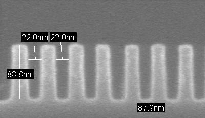
9 32nm and 22nm APF based SADP APF Properties: Integrity, Alignment SADP Scheme Performance, LER CDU: Line vs Space 9


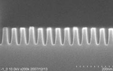
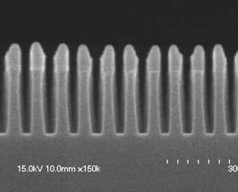
10 Self Aligned Double Patterning Scheme Print 32nm L&S with 193 dry Line Edge Roughness 1.5nm Photoresist Nitride 32 nm APF Oxide HM PhotoresistBefore After Trim Line Edge Roughness: nm 48 nm 34 nm Target 10


 26.5 25.7 Line (nm) 38.1 38.2 Core-Gap Delta (nm) 0.")
 3.1 2.5 Gap CDU 3σ (nm) 2.7 3.")

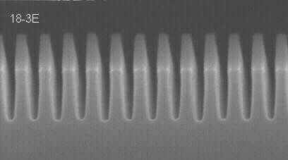
11 AMAT 3X SADP Performance Summary Core Gap Map 1: 92 Die 1 point per die After Bottom APF Etch Map 2: 4 full die, 8 partial 25 sub-die locations Map 3: 9 die 11 locations across array Wafer left Wafer center Wafer right B G F C A E H I D Top-view (Illustrative) 92 die 1 pt Wafer Edge Core (nm) Gap (nm) Line (nm) Core-Gap Delta (nm) Within Array LER (nm) LWR (nm) Core CDU 3σ (nm) Gap CDU 3σ (nm) Line CDU 3σ (nm) nm CD difference between core & gap CDU <2.4nm Litho LWR 3.5nm Bottom APF LWR 1.4nm APF AdvantEdge G5 Etch NDP Spacer 11
12 22nm Extendibility 12
 Slot 16 Slot 25 47.6 47.5 24.1 24.7 22.")

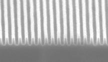
13 Summary of AMAT 22nm Spacer Mask Demonstrations: Core Gap 22nm Carbon Hardmask Top-view Immersion Litho Core Gap Line LER Core LER Gap Mean (nm) Slot 16 Slot nm 1.6 nm 1.7 nm 1.5 nm 3σ (nm) Slot 16 Slot *Results from 20 die measurement Demonstrated extendibility to 22nm CD Control of 2nm (3σ) LER <2nm 13
14 Application Demonstration 14

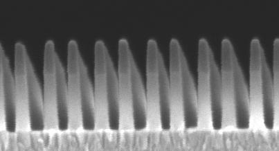
15 Applied Materials SADP Demonstrations Demonstrated Hardmask Patterning 32nm APF 22nm APF 34nm Self Aligned Dense Contact HM Demonstrated Applications: Hardmask for Contact Holes 32nm TANOS 32nm Oxide APF SiO2 32nm STI 22nm Copper Trench 22nm GDR for Logic 22nm STI Demonstrated on Flash critical dimension applications 15


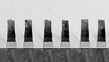
16 32nm SADP Process Flow for TANOS Flash SADP Etch 1 Process SADP Etch 2 Process CD Trim Top APF Etch Spacer Etch APF Strip-Out Etch Stop Etch SADP Etch 2 Process Metal Gate Etch Process HiK Etch Process Bottom APF Etch Oxide H.M. Etch W / WN / TaN Al2O3 and Si3N4 AMAT AdvantEdge etch chamber was used for all patterning etch steps SADP only required 2 etch steps for patterning 16
17 Core APF Automatic Process Control (APC) on G5 FF and FB Control ( Litho -> Trimming/BARC/APF Core Etch) No control FF+FB FF+FB O 2 Perturbation wafers were generated with an intentional CD variation to demonstrate FF and FB capability Litho CD Range 6.2nm and CD 1σ: 1.49nm Target CD is 38nm. Post etch CD (nm) FF & FB FF only Litho CD (nm) Wafers were split into three groups: Group 2 and 3: Incoming CD 1σ: 1.38nm Post etch CD 1σ: 0.57nm Post etch CD Wafer O2 12sccm 15sccm) Post etch CD w/ no FB (FF only) Demonstrated WTW CD control of 1.5% of target CD, despite intentional incoming CD variation and O 2 flow perturbation. 17
18 AMAT SADP Products 18


19 AMAT is ready for patterning 32nm & beyond Technologies available on proven manufacturing platforms to reduce risk and time to market Producer APF NDP PECVD AdvantEdge G5 Etch UVision SP Brightfield VeritySEM Metrology Demonstrated Spacer Self-Align Double Patterning 32nm Lines & Spaces with TANOS Stack, STI, oxide 22nm Lines & Spaces with oxide & gridded STI structures Achieved: LER [<1.7nm] CD Uniformity [<2nm] Overlay [<3nm] SADP is ready today for 32nm production Extendibility to 22nm is proven 19
20 Summary 20
21 SADP: Spacer Mask Approach APF Core Good LER Ashable no wet clean required Stable at high temp - spacer temp requirement relaxed as a result B C NDP Spacer >80% step coverage Good uniformity Good long range micro-loading performance A G5 for all SADP etch steps All-in-one chamber for all SADP etch steps & pattern etch Good CDU High productivity no warmup necessary APF Hardmask Good LER of 2nm Good line bending resistance 5:1 at 32nm; 4:1 at 22nm Full Portfolio Of Products Available For SADP Integration Schemes - Including UVision for defect analysis and Verity for CD measurement 21

22 22
COMPARISON OF EUV SINGLE EXPOSURE VS. 193i MULTIPLE PATTERING FOR N10 BEOL CHRISTOPHER J. WILSON
 COMPARISON OF EUV SINGLE EXPOSURE VS. 193i MULTIPLE PATTERING FOR N10 BEOL CHRISTOPHER J. WILSON - CONTRIBUTORS FORM ADVANCED LITHO AND CU-LOW-K IIAP PROGRAMS - ASML VELDHOVEN DEMO LAB FOR EXPOSURES EUV
DOUBLE PATTERNING CHALLENGES FOR 20nm TECHNOLOGY
 DOUBLE PATTERNING CHALLENGES FOR 20nm TECHNOLOGY SEMICON DRESDEN TechARENA OCTOBER 12 th 2011 Vincent Farys, Bertrand Le-Gratiet, Pierre-Jérôme Goirand STMicroelectronics Crolles 2 OUTLINE Lithography
Because Innovation Matters
 Because Innovation Matters Silicon Systems Group Toru Watanabe President, Applied Materials, Japan Semicon Japan November 30, 2010 Safe Harbor This presentation contains forward-looking statements, including
Outline. Double Patterning 11/6/17. Motivation Techniques Future of Double Patterning. Rasha El-Jaroudi November 7 th
 Double Patterning Rasha El-Jaroudi November 7 th 2017 reljaroudi@utexas.edu Outline Motivation Techniques Future of Double Patterning Rasha H. El-Jaroudi 2 1 Motivation Need to keep up with Moore s Law
SEMICON Europe October Pushing Lithography to the Limits. Patrick Wong imec
 SEMICON Europe October 2009 Pushing Lithography to the Limits imec 2009 1 Alternative double patterning processes : ready for (sub) 32nm hp? P. Wong, M. Maenhoudt, D. Vangoidsenhoven, V. Wiaux Outline
Overcoming Challenges in 3D NAND Volume Manufacturing
 Overcoming Challenges in 3D NAND Volume Manufacturing Thorsten Lill Vice President, Etch Emerging Technologies and Systems Flash Memory Summit 2017, Santa Clara 2017 Lam Research Corp. Flash Memory Summit
Nano-Imprint Lithography Infrastructure: Imprint Templates
 Nano-Imprint Lithography Infrastructure: Imprint Templates John Maltabes Photronics, Inc Austin, TX 1 Questions to keep in mind Imprint template manufacturability Resolution Can you get sub30nm images?
Readiness and Challenges of EUV Mask
 Panel Discussion: EUVL HVM Insertion and Scaling Readiness and Challenges of EUV Mask Takashi Kamo Toshiba Corporation Semiconductor & Storage Products Company Contents [1] Introduction [2] EUV Mask Defect
UV Nanoimprint Tool and Process Technology. S.V. Sreenivasan December 13 th, 2007
 UV Nanoimprint Tool and Process Technology S.V. Sreenivasan December 13 th, 2007 Agenda Introduction Need tool and process technology that can address: Patterning and CD control Alignment and Overlay Defect
Defect Reduction for Semiconductor Memory Applications Using Jet And Flash Imprint Lithography
 Defect Reduction for Semiconductor Memory Applications Using Jet And Flash Imprint Lithography Zhengmao Ye, Kang Luo, Xiaoming Lu, Brian Fletcher, Weijun Liu, Frank Xu, Dwayne LaBrake, Douglas Resnick,
Leveraging 300 mm Technology Solutions to Enable New MEMS Process Capabilities
 Leveraging 300 mm Technology Solutions to Enable New MEMS Process Capabilities Evan Patton Semicon Europa November 2017 Lam Research Corp. 1 Presentation Outline The Internet of Things (IoT) as a market
Advances in Roll-to-Roll Imprint Lithography for Display Applications Using Self Aligned Imprint Lithography. John G Maltabes HP Labs
 Advances in Roll-to-Roll Imprint Lithography for Display Applications Using Self Aligned Imprint Lithography John G Maltabes HP Labs Outline Introduction Roll to Roll Challenges and Benefits HP Labs Roll
Flexible Electronics Production Deployment on FPD Standards: Plastic Displays & Integrated Circuits. Stanislav Loboda R&D engineer
 Flexible Electronics Production Deployment on FPD Standards: Plastic Displays & Integrated Circuits Stanislav Loboda R&D engineer The world-first small-volume contract manufacturing for plastic TFT-arrays
PROGRESS OF UV-NIL TEMPLATE MAKING
 PROGRESS OF UV-NIL TEMPLATE MAKING Takaaki Hiraka, Jun Mizuochi, Yuko Nakanishi, Satoshi Yusa, Shiho Sasaki, Yasutaka Morikawa, Hiroshi Mohri, and Naoya Hayashi Electronic Device Laboratory, Dai Nippon
ABSTRACT. Keywords: 3D NAND, FLASH memory, Channel hole, Yield enhancement, Defect inspection, Defect reduction DISCUSSION
 Yield enhancement of 3D flash devices through broadband brightfield inspection of the channel hole process module Jung-Youl Lee a, Il-Seok Seo a, Seong-Min Ma a, Hyeon-Soo Kim a, Jin-Woong Kim a DoOh Kim
Advanced Display Manufacturing Technology
 Advanced Display Manufacturing Technology John Busch Vice President, New Business Development Display and Flexible Technology Group September 28, 2017 Safe Harbor This presentation contains forward-looking
The Challenges in Making NIL Master Templates
 The Challenges in Making NIL Master Templates Naoya Hayashi Dai Nippon Printing Co., Ltd. A Member of the ebeam Initiative 2011 Dai Nippon Printing Co.,Ltd. All Rights Reserved. OUTLINE Recent Progress
Applied Materials. 200mm Tools & Process Capabilities For Next Generation MEMS. Dr Michel (Mike) Rosa
 Rosa") Applied Materials 200mm Tools & Process Capabilities For Next Generation MEMS Dr Michel (Mike) Rosa 200mm MEMS Global Product / Marketing Manager, Components and Systems Group (CSG), Applied Global Services
Applied Materials 200mm Tools & Process Capabilities For Next Generation MEMS Dr Michel (Mike) Rosa 200mm MEMS Global Product / Marketing Manager, Components and Systems Group (CSG), Applied Global Services
AIXTRON in EXCILIGHT project
 AIXTRON SE AIXTRON in EXCILIGHT project Gintautas Simkus ABOUT AIXTRON 2 Who we are Headquarter based in Herzogenrath, Germany Worldwide presence with 14 sales/representatives offices and production facilities
HB LEDs & OLEDs. Complete thin film process solutions
 HB LEDs & OLEDs Complete thin film process solutions Get off to a flying start for all your LED thin film deposition and etch processes From 2 inch to 8 inch Manual or fully automated substrate handling
SEMICONDUCTOR TECHNOLOGY -CMOS-
 SEMICONDUCTOR TECHNOLOGY -CMOS- Fire Tom Wada 2011/12/19 1 What is semiconductor and LSIs Huge number of transistors can be integrated in a small Si chip. The size of the chip is roughly the size of nails.
Defense Technical Information Center Compilation Part Notice
 UNCLASSIFIED Defense Technical Information Center Compilation Part Notice ADPO1 1322 TITLE: Amorphous- Silicon Thin-Film Transistor With Two-Step Exposure Process DISTRIBUTION: Approved for public release,
Patterning Challenges for N7 and Beyond At a Crossroads. Steven Scheer. Director, Corporate Development Division TOKYO ELECTRON LIMITED
 Patterning Challenges for N7 and Beyond At a Crossroads Steven Scheer Director, Corporate Development Division TOKYO ELECTRON LIMITED Advanced Technologies in Accelerating Digital Era and IoT Forum Friday,
SEMICONDUCTOR TECHNOLOGY -CMOS-
 SEMICONDUCTOR TECHNOLOGY -CMOS- Fire Tom Wada What is semiconductor and LSIs Huge number of transistors can be integrated in a small Si chip. The size of the chip is roughly the size of nails. Currently,
STMicroelectronics NAND128W3A2BN6E 128 Mbit NAND Flash Memory Structural Analysis
 July 6, 2006 STMicroelectronics NAND128W3A2BN6E Structural Analysis For comments, questions, or more information about this report, or for any additional technical needs concerning semiconductor technology,
Pre SiGe Wet Cleans Development for sub 1x nm Technology Node
 Pre SiGe Wet Cleans Development for sub 1x nm Technology Node Akshey Sehgal, Anand Kadiyala, Michael DeVre and, Norberto Oliveria April 10 th, 2018 Background Due to higher aspect ratio features observed
The Transition to Patterned Media in Hard Disk Drives
 The Transition to Patterned Media in Hard Disk Drives The Evolution of Jet and Flash Imprint Lithography for Patterned Media DISKCON San Jose Sept 24 rd, 2009 Paul Hofemann, Vice President, HDD Future
Deep Silicon Etch Technology for Advanced MEMS Applications
 Deep Silicon Etch Technology for Advanced MEMS Applications Shenjian Liu, Ph.D. Managing Director, AMEC AMEC Company Profile and Product Line-up AMEC HQ, R&D and MF Facility in Shanghai AMEC Taiwan AMEC
Removing the Last Road Block of Deploying ILT into 10nm Node by Model-based Mask Data Preparation and Overlapped Shots
 Removing the Last Road Block of Deploying ILT into 10nm Node by Model-based Mask Data Preparation and Overlapped Shots Linyong (Leo) Pang Bo Su, Yohan Choi D2S, Inc. 1 193i Needed to be Extended and Extended
LEP400 Etch Depth Monitor Real-time, in-situ plasma etch depth monitoring and end point control plus co-linear wafer vision system
 LEP400 Etch Depth Monitor Real-time, in-situ plasma etch depth monitoring and end point control plus co-linear wafer vision system Base Configuration Etch Depth Monitoring LEP400 Recessed Window Plasma
Challenges in the design of a RGB LED display for indoor applications
 Synthetic Metals 122 (2001) 215±219 Challenges in the design of a RGB LED display for indoor applications Francis Nguyen * Osram Opto Semiconductors, In neon Technologies Corporation, 19000, Homestead
Inspection of 32nm imprinted patterns with an advanced e-beam inspection system
 Inspection of 32nm imprinted patterns with an advanced e-beam inspection system Hong Xiao, Long (Eric) Ma, Fei Wang, Yan Zhao, and Jack Jau Hermes Microvision, Inc., 1762 Automation Parkway, San Jose,
Reduction of Device Damage During Dry Etching of Advanced MMIC Devices Using Optical Emission Spectroscopy
 Reduction of Device Damage During Dry Etching of Advanced MMIC Devices Using Optical Emission Spectroscopy D. Johnson, R. Westerman, M. DeVre, Y. Lee, J. Sasserath Unaxis USA, Inc. 10050 16 th Street North
Multi-Shaped E-Beam Technology for Mask Writing
 Multi-Shaped E-Beam Technology for Mask Writing Juergen Gramss a, Arnd Stoeckel a, Ulf Weidenmueller a, Hans-Joachim Doering a, Martin Bloecker b, Martin Sczyrba b, Michael Finken b, Timo Wandel b, Detlef
Selective isotropic etching of Group IV semiconductors to enable gate all around device architectures
 TEL Technology Center, America, LLC - imec Selective isotropic etching of Group IV semiconductors to enable gate all around device architectures SPCC, April 10, 2018 S. Kal 1, C. Pereira 1, Y. Oniki 2,
AMOLED Manufacturing Process Report SAMPLE
 AMOLED Manufacturing Process Report SAMPLE 2018 AMOLED Manufacturing Process Report The report analyzes the structure and manufacturing process by dividing AMOLED into small & medium-sized rigid OLED,
Double Patterning OPC and Design for 22nm to 16nm Device Nodes
 Double Patterning OPC and Design for 22nm to 16nm Device Nodes Kevin Lucas, Chris Cork, Alex Miloslavsky, Gerry Luk-Pat, Xiaohai Li, Levi Barnes, Weimin Gao Synopsys Inc. Vincent Wiaux IMEC 1 Outline Introduction
Semiconductors Displays Semiconductor Manufacturing and Inspection Equipment Scientific Instruments
 Semiconductors Displays Semiconductor Manufacturing and Inspection Equipment Scientific Instruments Electronics 110-nm CMOS ASIC HDL4P Series with High-speed I/O Interfaces Hitachi has released the high-performance
Wafer Thinning and Thru-Silicon Vias
 Wafer Thinning and Thru-Silicon Vias The Path to Wafer Level Packaging jreche@trusi.com Summary A new dry etching technology Atmospheric Downstream Plasma (ADP) Etch Applications to Packaging Wafer Thinning
Standard Operating Manual
 Standard Operating Manual LAM490 AutoEtch System Copyright 11.2015 by Hong Kong University of Science & Technology. All rights reserved. Page 1 Contents 1. Picture and Location 2. Process Capabilities
(12) Patent Application Publication (10) Pub. No.: US 2016/ A1
 Patent Application Publication (10) Pub. No.: US 2016/ A1") (19) United States US 20160.042965A1 (12) Patent Application Publication (10) Pub. No.: US 2016/0042965 A1 Ha et al. (43) Pub. Date: Feb. 11, 2016 (54) METHODS FOR FORMING FINE PATTERNS Publication Classification
(19) United States US 20160.042965A1 (12) Patent Application Publication (10) Pub. No.: US 2016/0042965 A1 Ha et al. (43) Pub. Date: Feb. 11, 2016 (54) METHODS FOR FORMING FINE PATTERNS Publication Classification
Fabrication of Step and Flash TM Imprint Lithography Templates Using Commercial Mask Processes
 Fabrication of Step and Flash TM Imprint Lithography Templates Using Commercial Mask Processes Ecron Thompson, Peter Rhyins, Ron Voisin, S.V. Sreenivasan *, Patrick Martin Molecular Imprints, Inc., 1807C
High Performance Microprocessor Design and Automation: Overview, Challenges and Opportunities IBM Corporation
 High Performance Microprocessor Design and Automation: Overview, Challenges and Opportunities Introduction About Myself What to expect out of this lecture Understand the current trend in the IC Design
IC TECHNOLOGY Lecture 2.
 IC TECHNOLOGY Lecture 2. IC Integrated Circuit Technology Integrated Circuit: An integrated circuit (IC, a chip, or a microchip) is a set of electronic circuits on one small flat piece (or "chip") of semiconductor
2016, Amkor Technology, Inc.
 1 Standardization of Packaging for the Internet of Things Adrian Arcedera l VP of MEMS and Sensor Products 2 About Amkor Technology Amkor Technology, Inc. is one of the world's largest and most accomplished
Electron Beam Technology
 Electron Beam Technology Speed up! High Performance Electron Beam Lithography dedicated electron beam lithography To bridge cutting-edge research and nanofabrication, a dedicated nanolithography solution
Approaching Zero Etch Bias at Cr Etch Process
 Approaching Zero Etch Bias at Cr Etch Process Pavel Nesladek a ; Norbert Falk b ; Andreas Wiswesser a ; Renee Koch b ; Björn Sass a a Advanced Mask Technology Center, Rähnitzer Allee 9; 01109 Dresden,
Digital Light Processing
 A Seminar report On Digital Light Processing Submitted in partial fulfillment of the requirement for the award of degree of Bachelor of Technology in Computer Science SUBMITTED TO: www.studymafia.org SUBMITTED
SINGULATION BY PLASMA ETCHING. INTEGRATION TECHNIQUES TO ENABLE LOW DAMAGE, HIGH PRODUCTIVITY DICING.
 SINGULATION BY PLASMA ETCHING. INTEGRATION TECHNIQUES TO ENABLE LOW DAMAGE, HIGH PRODUCTIVITY DICING. Richard Barnett Dave Thomas Oliver Ansell ABSTRACT Plasma dicing has rapidly gained traction as a viable
SciFi A Large Scintillating Fibre Tracker for LHCb
 SciFi A Large Scintillating Fibre Tracker for LHCb Roman Greim on behalf of the LHCb-SciFi-Collaboration 14th Topical Seminar on Innovative Particle Radiation Detectors, Siena 5th October 2016 I. Physikalisches
Parts of dicing machines for scribing or scoring semiconductor wafers , , , , ,
 US-Rev3 26 March 1997 With respect to any product described in or for Attachment B to the Annex to the Ministerial Declaration on Trade in Information Technology Products (WT/MIN(96)/16), to the extent
Summary of Selected EMCR650 Projects for Fall 2005 Mike Aquilino Dr. Lynn Fuller
 ROCHESTER INSTITUTE OF TECHNOLOGY MICROELECTRONIC ENGINEERING Summary of Selected EMCR650 Projects for Fall 2005 Mike quilino Dr. Lynn Fuller http://www.rit.edu/~lffeee 82 Lomb Memorial Drive Rochester,
ADVANCED MICRO DEVICES, 2 CADENCE DESIGN SYSTEMS
 METHODOLOGY FOR ANALYZING AND QUANTIFYING DESIGN STYLE CHANGES AND COMPLEXITY USING TOPOLOGICAL PATTERNS JASON CAIN 1, YA-CHIEH LAI 2, FRANK GENNARI 2, JASON SWEIS 2 1 ADVANCED MICRO DEVICES, 2 CADENCE
Introduction and recent results of Multi-beam mask writer MBM-1000
 Introduction and recent results of Multi-beam mask writer MBM-1000 Hiroshi Matsumoto, Yasuo Kato, Munehiro Ogasawara, Hirokazu Yamada February 23 rd, 2016 Member of the ebeam Initiative NFT s mask writer
FLEX2017 June, Monterey, USA Dr Mike Cowin, CMO, SmartKem.
 FLEX2017 June, Monterey, USA Dr Mike Cowin, CMO, SmartKem. FLEX2017 June, Monterey, USA Dr Mike Cowin, CMO, SmartKem. EU H2020 FLEXTRANs Grant Objectives A 24 month project (started September 2016) (Grant
Layers of Innovation: How Signal Chain Innovations are Creating Analog Opportunities in a Digital World
 The World Leader in High Performance Signal Processing Solutions Layers of Innovation: How Signal Chain Innovations are Creating Analog Opportunities in a Digital World Dave Robertson-- VP of Analog Technology
EUV Mask and Wafer Defectivity: Strategy and Evaluation for Full Die Defect Inspection
 EUV Mask and Wafer Defectivity: Strategy and Evaluation for Full Die Defect Inspection Ravi Bonam 1, Hung-Yu Tien 2, Acer Chou 2, Luciana Meli 1, Scott Halle 1, Ivy Wu 2, Xiaoxia Huang 2, Chris Lei 2,
New Worlds for Polymers: Organic Transistors, Light Emitting Diodes, and Optical Waveguides Ed Chandross
 New Worlds for Polymers: Organic Transistors, Light Emitting Diodes, and Optical Waveguides Ed Chandross Materials Chemistry, LLC 1 Polymers in the Electronic Industry Enabling Materials Active Materials?
Advancements in Acoustic Micro-Imaging Tuesday October 11th, 2016
 Central Texas Electronics Association Advancements in Acoustic Micro-Imaging Tuesday October 11th, 2016 A review of the latest advancements in Acoustic Micro-Imaging for the non-destructive inspection
CMP and Current Trends Related to Advanced Packaging
 CMP and Current Trends Related to Advanced Packaging Robert L. Rhoades, Ph.D. NCCAVS TFUG-CMPUG Joint Meeting June 7, 2017 Semiconductor Equipment Spare Parts and Service CMP Foundry Foundry Click to edit
IC Mask Design. Christopher Saint Judy Saint
 IC Mask Design Essential Layout Techniques Christopher Saint Judy Saint McGraw-Hill New York Chicago San Francisco Lisbon London Madrid Mexico City Milan New Delhi San Juan Seoul Singapore Sydney Toronto
Forward-Looking Statements
 Forward-Looking Statements Information in this presentation regarding MagnaChip s forecasts, business outlook, expectations and beliefs are forward-looking statements within the meaning of the Private
MagnaChip HV7161SP 1.3 Megapixel CMOS Image Sensor Process Review
 September 21, 2005 MagnaChip HV7161SP 1.3 Megapixel Process Review For questions, comments, or more information about this report, or for any additional technical needs concerning semiconductor technology,
Monolithic Optoelectronic Integration of High- Voltage Power FETs and LEDs
 Monolithic Optoelectronic Integration of High- Voltage Power FETs and LEDs, Zhongda Li, Robert Karlicek and T. Paul Chow Smart Lighting Engineering Research Center Rensselaer Polytechnic Institute, Troy,
Freescale SPC5604BF1CLL6 Embedded NOR Flash with M27V Die Markings 32 Bit Power Architecture Automotive Microcontroller 90 nm Logic Process
 Freescale SPC5604BF1CLL6 Embedded NOR Flash with M27V Die Markings 32 Bit Power Architecture Automotive Microcontroller 90 nm Logic Process Process Review 3685 Richmond Road, Suite 500, Ottawa, ON K2H
EECS150 - Digital Design Lecture 2 - CMOS
 EECS150 - Digital Design Lecture 2 - CMOS January 23, 2003 John Wawrzynek Spring 2003 EECS150 - Lec02-CMOS Page 1 Outline Overview of Physical Implementations CMOS devices Announcements/Break CMOS transistor
Principles of Electrostatic Chucks 6 Rf Chuck Edge Design
 Principles of Electrostatic Chucks 6 Rf Chuck Edge Design Overview This document addresses the following chuck edge design issues: Device yield through system uniformity and particle reduction; System
An Overview of the Performance Envelope of Digital Micromirror Device (DMD) Based Projection Display Systems
 Based Projection Display Systems") An Overview of the Performance Envelope of Digital Micromirror Device (DMD) Based Projection Display Systems Dr. Jeffrey B. Sampsell Texas Instruments Digital projection display systems based on the DMD
An Overview of the Performance Envelope of Digital Micromirror Device (DMD) Based Projection Display Systems Dr. Jeffrey B. Sampsell Texas Instruments Digital projection display systems based on the DMD
Spatial Light Modulators XY Series
 Spatial Light Modulators XY Series Phase and Amplitude 512x512 and 256x256 A spatial light modulator (SLM) is an electrically programmable device that modulates light according to a fixed spatial (pixel)
CS250 VLSI Systems Design
 CS250 VLSI Systems Design Fall 2012 John Wawrzynek, Jonathan Bachrach with Krste Asanovic, John Lazzaro and Rimas Avizienis (TA) Why CS250 and not EE250 Put IC design expertise into the hands of those
Integrated Circuit Design ELCT 701 (Winter 2017) Lecture 1: Introduction
 Lecture 1: Introduction") 1 Integrated Circuit Design ELCT 701 (Winter 2017) Lecture 1: Introduction Assistant Professor Office: C3.315 E-mail: eman.azab@guc.edu.eg 2 Course Overview Lecturer Teaching Assistant Course Team E-mail:
1 Integrated Circuit Design ELCT 701 (Winter 2017) Lecture 1: Introduction Assistant Professor Office: C3.315 E-mail: eman.azab@guc.edu.eg 2 Course Overview Lecturer Teaching Assistant Course Team E-mail:
Spring Probes and Probe Cards for Wafer-Level Test. Jim Brandes Multitest. A Comparison of Probe Solutions for an RF WLCSP Product
 Session 6 AND, AT THE WAFER LEVEL For many in the industry, performing final test at the wafer level is still a novel idea. While providing some much needed solutions, it also comes with its own set of
ABSTRACT 1 INTRODUCTION
 Novel lithography technique using an ASML Stepper/Scanner for the manufacture of display devices in MEMS world ASML US, Inc Special Applications, 6580 Via Del Oro San Jose, CA 95119 Keith Best, Pankaj
A new Scintillating Fibre Tracker for LHCb experiment
 A new Scintillating Fibre Tracker for LHCb experiment Alexander Malinin, NRC Kurchatov Institute on behalf of the LHCb-SciFi-Collaboration Instrumentation for Colliding Beam Physics BINP, Novosibirsk,
Facedown Terminations Improve Ripple Current Capability
 Facedown Terminations Improve Ripple Current Capability John Prymak 1,Peter Blais 2, Bill Long 3 KEMET Electronics Corp. PO Box 5928, Greenville, SC 29606 1 66 Concord St., Suite Z, Wilmington, MA 01887
Solderability Test Summary Report
 Date: 05/27/05 Page 1 Of 11 PCA Manufacturing Technologies & Engineering Services Solderability Test Summary Report Lucent Technologies Work Order: MT-WO-5191 Reliability Physics Group Customer PO: CC
How UV selectable illumination inspection tool and methodologies can accelerate learning curve of advanced technologies
 How UV selectable illumination inspection tool and methodologies can accelerate learning curve of advanced technologies V. Twines, C. Archambuult, B. Hinschberger, E. Rouchouze ST Microelectronic Crolles
Digital Integrated Circuits EECS 312
 14 12 10 8 6 Fujitsu VP2000 IBM 3090S Pulsar 4 IBM 3090 IBM RY6 CDC Cyber 205 IBM 4381 IBM RY4 2 IBM 3081 Apache Fujitsu M380 IBM 370 Merced IBM 360 IBM 3033 Vacuum Pentium II(DSIP) 0 1950 1960 1970 1980
The Company. A leading OLED player
 The Company A leading OLED player Novaled is the company to trade with, work for and invest in. Our company focuses on proprietary organic materials and complementary innovative technologies for superior
OV µm Pixel Size Back Side Illuminated (BSI) 5 Megapixel CMOS Image Sensor
 5 Megapixel CMOS Image Sensor") OmniVision OV5642 1.4 µm Pixel Size Back Side Illuminated (BSI) 5 Megapixel CMOS Image Sensor Circuit Analysis of the Pixel Array, Row Control, Column Readout, Analog Front End, and Pipelined A/D Converter
OmniVision OV5642 1.4 µm Pixel Size Back Side Illuminated (BSI) 5 Megapixel CMOS Image Sensor Circuit Analysis of the Pixel Array, Row Control, Column Readout, Analog Front End, and Pipelined A/D Converter
Abstract. Keywords INTRODUCTION. Electron beam has been increasingly used for defect inspection in IC chip
 Abstract Based on failure analysis data the estimated failure mechanism in capacitor like device structures was simulated on wafer in Front End of Line. In the study the optimal process step for electron
projectors, head mounted displays in virtual or augmented reality use, electronic viewfinders
 Beatrice Beyer Figure 1. (OLED) microdisplay with a screen diagonal of 16 mm. Figure 2. CMOS cross section with OLED on top. Usually as small as fingernails, but of very high resolution Optical system
Automation in Semiconductor Manufacturing IEDM, San Francisco, 1982 Keynote Speech
 Automation in Semiconductor Manufacturing IEDM, San Francisco, 1982 Keynote Speech Commentary Alongside ISSCC, IEDM is the most traditional academic conference in the semiconductor field, and it is held
CCD Element Linear Image Sensor CCD Element Line Scan Image Sensor
 1024-Element Linear Image Sensor CCD 134 1024-Element Line Scan Image Sensor FEATURES 1024 x 1 photosite array 13µm x 13µm photosites on 13µm pitch Anti-blooming and integration control Enhanced spectral
Auto classification and simulation of mask defects using SEM and CAD images
 Auto classification and simulation of mask defects using SEM and CAD images Tung Yaw Kang, Hsin Chang Lee Taiwan Semiconductor Manufacturing Company, Ltd. 25, Li Hsin Road, Hsinchu Science Park, Hsinchu
Reliability of Level 1 and Level 2 Packaging in Solid-State Lighting Devices
 Reliability of Level 1 and Level 2 Packaging in Solid-State Lighting Devices Lynn Davis, PhD Fellow, RTI International December 8, 2016 1 RTI International is a registered trademark and a trade name of
Lossless Compression Algorithms for Direct- Write Lithography Systems
 Lossless Compression Algorithms for Direct- Write Lithography Systems Hsin-I Liu Video and Image Processing Lab Department of Electrical Engineering and Computer Science University of California at Berkeley
Verification of HBM through Direct Probing on MicroBumps
 Verification of HBM through Direct Probing on MicroBumps FormFactor Sung Wook Moon SK hynix Outline HBM market HBM test flow Device structure overview Key test challenges addressed Signal delivery and
Layout Analysis Analog Block
 Layout Analysis Analog Block Sample Report Analysis from an HD Video/Audio SoC For any additional technical needs concerning semiconductor and electronics technology, please call Sales at Chipworks. 3685
NXP t505f Smart Card RFID Die Embedded NOR Flash Die From Smart Card World MIFARE Ultralight C
 NXP t505f Smart Card RFID Die Die From Smart Card World MIFARE Ultralight C Custom Process Analysis For comments, questions, or more information about this report, or for any additional technical needs
1. Publishable summary
 1. Publishable summary 1.1. Project objectives. The target of the project is to develop a highly reliable high brightness conformable low cost scalable display for demanding applications such as their
21 rue La Noue Bras de Fer Nantes - France Phone : +33 (0) website :
 website :") 21 rue La Noue Bras de Fer - 44200 Nantes - France Phone : +33 (0) 240 180 916 - email : info@systemplus.fr - website : www.systemplus.fr 2012 September - Version 1 Written by: Maher Sahmimi DISCLAIMER
21 rue La Noue Bras de Fer - 44200 Nantes - France Phone : +33 (0) 240 180 916 - email : info@systemplus.fr - website : www.systemplus.fr 2012 September - Version 1 Written by: Maher Sahmimi DISCLAIMER
Recent results of Multi-beam mask writer MBM-1000
 Recent results of Multi-beam mask writer MBM-1000 Hiroshi Matsumoto, Hiroshi Yamashita, Hideo Inoue, Kenji Ohtoshi, Hirokazu Yamada Member of the ebeam Initiative 1 NFT s mask writer roadmap 2016 Device
ADA-4789 Data Sheet Description Features Specifications Package Marking and Pin Connections 4GX Applications
 ADA-789 Silicon Bipolar Darlington Amplifier Data Sheet Description Avago Technologies ADA-789 is an economical, easyto-use, general purpose silicon bipolar RFIC gain block amplifiers housed in SOT-89
9 rue Alfred Kastler - BP Nantes Cedex 3 - France Phone : +33 (0) website :
 website :") 9 rue Alfred Kastler - BP 10748-44307 Nantes Cedex 3 - France Phone : +33 (0) 240 180 916 - email : info@systemplus.fr - website : www.systemplus.fr January 2012 Written by: Maher SAHMIMI DISCLAIMER :
9 rue Alfred Kastler - BP 10748-44307 Nantes Cedex 3 - France Phone : +33 (0) 240 180 916 - email : info@systemplus.fr - website : www.systemplus.fr January 2012 Written by: Maher SAHMIMI DISCLAIMER :
Study of Pattern Area Reduction. with FinFET and SGT for LSI
 Contemporary Engineering Sciences, Vol. 6, 2013, no. 4, 177-190 HIKRI Ltd, www.m-hikari.com Study of Pattern rea Reduction with FinFET and SGT for LSI Takahiro Kodama Japan Process Development Co., Ltd.
Technology Overview LTCC
 Sheet Code RFi0604 Technology Overview LTCC Low Temperature Co-fired Ceramic (LTCC) is a multilayer ceramic substrate technology that allows the realisation of multiple embedded passive components (Rs,
Wafer defects can t hide from
 WAFER DEFECTS Article published in Issue 3 2016 Wafer defects can t hide from Park Systems Atomic Force Microscopy (AFM) leader Park Systems has simplified 300mm silicon wafer defect review by automating
Transforming Electronic Interconnect Breaking through historical boundaries Tim Olson Founder & CTO
 Transforming Electronic Interconnect Breaking through historical boundaries Tim Olson Founder & CTO Remember when? There were three distinct industries Wafer Foundries SATS EMS Semiconductor Devices Nanometers
CCD 143A 2048-Element High Speed Linear Image Sensor
 A CCD 143A 2048-Element High Speed Linear Image Sensor FEATURES 2048 x 1 photosite array 13µm x 13µm photosites on 13µm pitch High speed = up to 20MHz data rates Enhanced spectral response Low dark signal