Features. Specification Min. Typ. Max. Input Return Loss MHz db. Output Return Loss MHz db. Reverse Isolation -22.
|
|
|
- Magdalen Williams
- 6 years ago
- Views:
Transcription
 package.")
1 Product Description RG512 is a low current and low noise Gain Block Amplifier in a low-cost surface mount package and provides 30dBm high OIP3 and 1.62dB Noise Figure at 1900MHz. It is fabricated on a compound semiconductor material and conventional device technology. RG512 is available in a lead-free / green / RoHS-compliant SOT363(SC70) package. The performance is targeted for use as a receiver and transmitter in wireless infrastructure system where high linearity and low noise is required. Internal active bias circuitry allows RG512 to maintain high linearity and gain performance over temperature and operate directly off a single +3V supply. All devices are 100% RF and DC tested and internally matched to 50 ohms without additional external components. Features High OIP3 30dBm at 1900MHz 18.9dB Gain at 900MHz P1dB=20dBm at 1900MHz 1.62dB Noise Figure at 1900MHz Unconditionally stable Single 3.3V supply, 27mA current No dropping resistor required Industry standard SOT363(SC70) package Lead-free, RoHS compliant, Green Applications Broadband Gain Block Wireless infrastructure Cellular, PCS, GSM, WCDMA, WiBro, LTE Component Diagram GND GND RF IN 512XX G11XX SOT-363(SC70) RF OUT GND GND Parameter Specification Min. Typ. Max. Condition Units MHz db Small Signal Gain MHz db MHz db Output power at 1-dB Compression Third Order Intercept Point MHz dbm MHz dbm MHz dbm MHz dbm Input Return Loss MHz db Output Return Loss MHz db Reverse Isolation MHz db Noise Figure MHz db Device Voltage 3.3 V Device current (Icq) ma Thermal Resistance 41.6 Test condition: Vcc=3.3V, I D =27mA Typ., OIP 3 Tone Spacing=1MHz, P out per tone=6dbm T L =25 C, Z S =Z L =50 Junction to lead C/W 1
2 Absolute Maximum Ratings Parameter Rating Unit Max Device Voltage(V D ) 5.0 V Max Device Current(I D ) 60 ma Max RF Input Power 10 dbm Max Operating Dissipated Power 0.3 W Junction Temperature(T J ) +150 C Operating Temperature(T L ) -40 to +85 C Storage Temperature -65 to +150 C ESD Sensitivity(HBM) Moisture Sensitivity Level Class 1A MSL1 Typical Electrical Specification Parameter 700MHz 900MHz 1900MHz 2140MHz 2650MHz Unit S db OIP dbm P1dB dbm S db S db S db NF db Test condition: Vcc=3.3V, I D =27mA Typ., OIP 3 Tone Spacing=1MHz, P out per tone=6dbm T L =25 C, Z S =Z L =50 2


3 700~900MHz Reference Application Circuit Parameter/Freq.(MHz) Unit Small Signal Gain db S db S db Output P1dB dbm Output OIP3* dbm BOM Value BOM Value BOM Value C1 100pF C4 1000pF L1 22nH C2 100pF C5 10uF Noise Figure db Icq 27 ma C3 100pF Vcc 3.3 V *Width and Length of Micro-strip line dimension in mm[mil] * Pout=6dBm/tone S-Parameter Over Temperature vs. Freq. at 700~900MHz 3


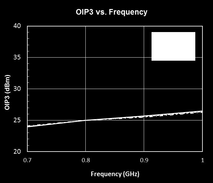
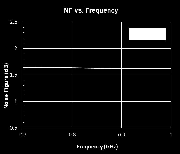
4 P1dB, OIP3 and Noise Figure Performance at 700~900MHz 4
 1800 1900 2140 Unit Small Signal Gain 14.4 14.2 13.5 db S11-21.8-22.1-19.")


5 1800~2200MHz Reference Application Circuit Parameter/Freq.(MHz) Unit Small Signal Gain db S db S db Output P1dB dbm Output OIP3* dbm BOM Value BOM Value BOM Value C1 100pF C4 1000pF L1 10nH C2 100pF C5 10uF Noise Figure db Icq 27 ma C3 100pF Vcc 3.3 V *Width and Length of Micro-strip line dimension in mm[mil] * Pout=6dBm/tone S-Parameter Over Temperature vs. Freq. at 1800~2200MHz 5

6 P1dB, OIP3 and Noise Figure Performance at 1800~2200MHz 6
 2300 2650 2750 Unit Small Signal Gain 12.7 11.7 11.0 db S11-18.4-17.7-18.")


7 2300~2700MHz Reference Application Circuit Parameter/Freq.(MHz) Unit Small Signal Gain db S db S db Output P1dB dbm Output OIP3* dbm BOM Value BOM Value BOM Value C1 100pF C4 1000pF L1 10nH C2 100pF C5 10uF Noise Figure db Icq 27 ma C3 100pF Vcc 3.3 V *Width and Length of Micro-strip line dimension in mm[mil] * Pout=6dBm/tone S-Parameter Over Temperature vs. Freq. at 2300~2700MHz 7


8 P1dB, OIP3 and Noise Figure Performance at 2300~2700MHz 8
9 Package Mark and Dimensions DIMENSIONS MILLIMETER DIMENSIONS INCH Symbol MIN NOM MAX MIN NOM MAX A B C D E F PCB Substrate Information[mm] Dielectric Constant FR-4/4.6 Dielectric Height 0.037[0.93] Copper Thickness 1 oz. 9
Description. Specifications
 PW21 Wideband Block Features to 6MHz 21.4dB @ 7MHz P1dB 16.3dBm @ 23MHz OIP3 3.6dBm @ 19MHz Lead-free / Green / compliant SOT-89 Package Applications Base station / Repeater / Mobile / Automotive / Military
Typical Performance 1. 1 Device performance _ measured on a BeRex evaluation board at 25 C, 50 Ω system.
 Device Features 3 ~ 3.2V supply No Dropping Resistor Required No matching circuit needed Lead-free/Green/RoHS compliant SOT-363 package Application: Driver Amplifier, Cellular, PCS, GSM, UMTS, WCDMA, Wireless
Typical Performance 1. 1 Device performance _ measured on a BeRex evaluation board at 25 C, 50 Ω system.
 Device Features Single Fixed 3V supply No Dropping Resistor Required No matching circuit needed Lead-free/Green/RoHS compliant SOT-363 package Application: Driver Amplifier, Cellular, PCS, GSM, UMTS, WCDMA,
Typical Performance 1. 1 Device performance _ measured on a BeRex evaluation board at 25 C, 50 Ω system.
 Device Features NF = 0.91 db @ 900MHz at RF connectors of Demo board Gain = 22.0 db @ 900 MHz OIP3 = 36.0 dbm @ 1900MHz, 38.0 dbm @ 2450MHz Output P1 db = 20.5 dbm @ 900/1900/2140 MHz 5V/75mA, MTTF > 100
GHz Wideband High Linearity LNA Gain Block. Typical Performance 1
 Device Features Internally matched to 50 ohms This can be operated at Vd of 3.3V and 4.4V 37.0 dbm Output IP3 at 5dBm/tone at 1900MHz 15.5 db Gain at 1900MHz 22.0 dbm P1dB at 1900 MHz 1.6 db NF at 1900MHz
Typical Performance 1. 1 Device performance _ measured on a BeRex evaluation board at 25 C, 50 Ω system.
 Device Features Single Fixed 3V supply No Dropping Resistor Required No matching circuit needed Lead-free/Green/RoHS compliant SOT-363 package Application: Driver Amplifier, Cellular, PCS, GSM, UMTS, WCDMA,
Typical Performance 1. 1 Device performance _ measured on a BeRex evaluation board at 25 C, 50 Ω system.
 Device Features Single Fixed 3V supply No Dropping Resistor Required No matching circuit needed Lead-free/Green/RoHS compliant SOT-363 package Application: Driver Amplifier, Cellular, PCS, GSM, UMTS, WCDMA,
Not recommended for new designs
 Device Features NF = 0.7 db @ 900MHz at RF connectors of Demo board Gain = 19.0 db @ 900 MHz OIP3 = 36.0 dbm @ 1900MHz, 2450MHz Output P1 db = 21.0 dbm @ 900MHz, 22.0 dbm @2450MHz 5V/48mA, MTTF > 100 Years,
Typical Performance 1. 2 OIP3 _ measured on two tones with a output power 8 dbm/ tone, F2 F1 = 1 MHz. +5V. RFout. Absolute Maximum Ratings
 Device Features OIP3 = 41.5 dbm @ 500 MHz Gain = 27 db @ 140 MHz Output P1 db = 21 dbm @ 140 MHz NF = 2.7 @ 70MHz at Demo Board Product Description BeRex s BIG8 is a high performance InGaP/ GaAs HBT MMIC
Typical Performance 1. 1 Device performance _ measured on a BeRex evaluation board at 25 C, 50 Ω system.
 Device Features OIP3 = 28 dbm @ 1900 MHz Gain = 16 db @ 1900 MHz Output P1 db = 15.5 dbm @ 1900 MHz 50 Ω Cascadable Patented temperature compensation Lead-free/RoHS-compliant SOT-89 SMT package Product
Typical Performance 1. 1 Device performance _ measured on a BeRex evaluation board at 25 C, 50 Ω system.
 Device Features OIP3 = 43.0 dbm @ 70 MHz Gain = 17.5 db @ 70 MHz Output P1 db = 20.5 dbm @ 70 MHz 50 Ω Cascadable Patented temperature compensation Patented over voltage protection Lead-free/RoHS-compliant
Typical Performance 1. 1 Device performance _ measured on a BeRex evaluation board at 25 C, 50 Ω system.
 Device Features OIP3 = 32.0 dbm @ 1900 MHz Gain = 22.2 db @ 1900 MHz Output P1 db = 19.0 dbm @ 1900 MHz 50 Ω Cascadable Patented temperature compensation Patented Over Voltage Protection Circuit Lead-free/RoHS-compliant
Typical Performance 1. 1 Device performance _ measured on a BeRex evaluation board at 25 C, 50 Ω system.
 Device Features OIP3 = 44.0 dbm @ 70 MHz Gain = 20.3 db @ 70 MHz Output P1 db = 23.5 dbm @ 70 MHz 50 Ω Cascadable Patented over voltage protection Lead-free/RoHS-compliant SOT-89 SMT package Product Description
Typical Performance 1. 1 Device performance _ measured on a BeRex evaluation board at 25 C, 50 Ω system.
 Device Features OIP3 = 32.5 dbm @ 1900 MHz Gain = 20.9 db @ 1900 MHz Output P1 db = 18.8 dbm @ 1900 MHz 50 Ω Cascadable Patented temperature compensation Patented Over Voltage Protection Circuit Lead-free/RoHS-compliant
OBSOLETE HMC215LP4 / 215LP4E. GaAs MMIC MIXER w/ INTEGRATED LO AMPLIFIER, GHz. Typical Applications. Features. Functional Diagram
 v1.111 LO AMPLIFIER, 1.7-4. GHz Typical Applications The HMC215LP4 / HMC215LP4E is ideal for Wireless Infrastructure Applications: PCS / 3G Infrastructure Base Stations & Repeaters WiMAX & WiBro ISM &
HMC581LP6 / 581LP6E MIXERS - SMT. HIGH IP3 RFIC DUAL DOWNCONVERTER, MHz. Typical Applications. Features. Functional Diagram
 Typical Applications The HMC1LP6 / HMC1LP6E is ideal for Wireless Infrastructure Applications: GSM, GPRS & EDGE CDMA & W-CDMA Cellular / 3G Infrastructure Functional Diagram Features +26 dbm Input IP3
AH125 ½ W High Linearity InGaP HBT Amplifier
 Product Overview The is a high dynamic range driver amplifier in a low-cost surface mount package. The InGaP/GaAs HBT is able to achieve high performance across a broad range with +45 dbm OIP3 and +28
Typical Performance 1. 1 Device performance _ measured on a BeRex evaluation board at 25 C, 50 Ω system.
 Device Features OIP3 = 39.0 dbm @ 70 MHz Gain = 24 db @ 70 MHz Output P1 db = 20.5 dbm @ 70 MHz 50 Ω Cascadable Patented temperature compensation Lead-free/RoHS-compliant SOT-89 SMT package Product Description
2 OIP3 _ measured on two tones with a output power 8 dbm/ tone, F2 F1 = 1 MHz. Absolute Maximum Ratings
 Device Features OIP3 = 41 dbm @ 14 MHz Gain = 2. db @ 14 MHz Output P1 db = 2. dbm @ 14 MHz NF = 2.7 @ 14MHz at Demo Board Ω Cascadable Lead-free/RoHS-compliant SOT-89 SMT package Typical Performance 1
Typical Performance 1. 2 OIP3 _ measured with two tones at an output of 7 dbm per tone separated by 1 MHz. Absolute Maximum Ratings
 Device Features OIP3 = 32 dbm @ 1900 MHz Gain = 21.5 db @ 1900 MHz Output P1 db = 19 dbm @ 1900 MHz 50 Ω Cascadable Patented temperature compensation Lead-free/RoHS-compliant SOT-89 SMT package Product
Monolithic Amplifier GVA-60+ Flat Gain, High IP to 5 GHz. The Big Deal
 Flat Gain, High IP3 Monolithic Amplifier 50Ω 0.01 to 5 GHz The Big Deal Excellent Gain Flatness and Return Loss over 50-1000 MHz High IP3 vs. DC Power consumption Broadband High Dynamic Range without external
Typical Performance 1. 2 OIP3 _ measured with two tones at an output of 9 dbm per tone separated by 1 MHz. Absolute Maximum Ratings
 Device Features OIP3 = 35.5 dbm @ 1900 MHz Gain = 16 db @ 1900 MHz Output P1 db = 19.7 dbm @ 1900 MHz 50 Ω Cascadable Patented temperature compensation Lead-free/RoHS-compliant SOT-89 SMT package Product
1 Watt High Linearity, High Gain InGaP HBT Amplifier. Product Description
 Product Features 18 24 MHz 24.7 db Gain +3 dbm P1dB +46 dbm Output IP3 +V Single Positive Supply Internal Active Bias Lead-free/ RoHS-compliant SOIC-8 & 4xmm DFN Package Applications Mobile Infrastructure
Typical Performance 1. 1 Device performance _ measured on a BeRex evaluation board at 25 C, 50 Ω system.
 Device Features OIP3 = 30 dbm @ 1900 MHz Gain = 16.4 db @ 1900 MHz Output P1 db = 17 dbm @ 1900 MHz 50 Ω Cascadable Patented temperature compensation Lead-free/RoHS-compliant SOT-89 SMT package Product
Typical Performance 1. 1 Device performance _ measured on a BeRex evaluation board at 25 C, 50 Ω system.
 Device Features OIP3 = 35 dbm @ 1900 MHz Gain = 16 db @ 1900 MHz Output P1 db = 19.5 dbm @ 1900 MHz 50 Ω Cascadable Patented temperature compensation Lead-free/RoHS-compliant SOT-89 SMT package Product
Typical Performance 1
 Device Features Internally matched to 50 ohms Operated at 3.0V and 5.0V 37.5 dbm Output IP3 at 0dBm/tone at 700MHz 22.5dB Gain at 700MHz 21.1dBm P1dB at 700 MHz 0.40 db NF at 700MHz on evaluation board
Preliminary Datasheet
 Device Features Operated at 3.0V and 5.0V 35.5 dbm Output IP3 at 0dBm/tone at 3500MHz 16.4 db Gain at 3500 MHz 20.1 dbm P1dB at 3500MHz 0.67 db NF at 3500MHz Fast shut down to support TDD systems Lead-free/Green/RoHS
Typical Performance 1
 Device Features Internally matched to 50 ohms Operated at 3.0V and 5.0V 36.2 dbm Output IP3 at 0dBm/tone at 1850 MHz 18.5dB Gain at 1850MHz 19.6dBm P1dB at 1850MHz 0.65 db NF at 1850MHz on evaluation board
FH1. Functional Diagram. Product Description. Product Features. Applications. Typical Performance (6) Specifications (1) Absolute Maximum Rating
 Specifications (1) Absolute Maximum Rating") FH Product Features 5 4 MHz Low Noise Figure 8 db Gain +4 dbm OIP3 + dbm PdB Single or Dual Supply Operation Lead-free/Green/RoHS-compliant SOT-89 Package MTTF > years Applications Mobile Infrastructure
FH Product Features 5 4 MHz Low Noise Figure 8 db Gain +4 dbm OIP3 + dbm PdB Single or Dual Supply Operation Lead-free/Green/RoHS-compliant SOT-89 Package MTTF > years Applications Mobile Infrastructure
Typical Performance 1. 1 Device performance _ measured on a BeRex evaluation board at 25 C, 50 Ω system.
 Device Features OIP3 = 35 dbm @ 1900 MHz Gain = 13.3 db @ 1900 MHz Output P1 db = 18.5 dbm @ 1900 MHz 50 Ω Cascadable Patented temperature compensation Lead-free/RoHS-compliant SOT-89 SMT package Product
Features. = +25 C, LO = 0 dbm, Vcc = Vcc1, 2, 3 = +5V, G_Bias = +2.5V *
 Typical Applications The is Ideal for: Cellular/3G & LTE/WiMAX/4G Basestations & Repeaters GSM, CDMA & OFDM Transmitters and Receivers Features High Input IP3: +38 dbm 8 db Conversion Loss @ 0 dbm LO Optimized
50~100MHz. 100~210MHz C2 1nF. Operating Case Temperature -40 to +85 Storage Temperature -55 to +155 Junction Temperature +126 Operating Voltage
 0.7~1.4GHz High IIP3 GaAs MMIC with Integrated LO AMP Device Features +31.7 dbm Input IP3 8.8dB Conversion Loss Integrated LO Driver -2 to +2dBm LO drive level Available 3.3V to 5V single voltage MSL 1,
* Notices. Operating Case Temperature -40 to +85 Storage Temperature -55 to +155 Junction Temperature +126 Operating Voltage.
 1.7~2.7GHz High IIP3 GaAs MMIC with Integrated LO AMP Device Features +33.9 dbm Input IP3 8.3dB Conversion Loss Integrated LO Driver -2 to +4dBm LO drive level Available 3.3V to 5V single voltage MSL 1,
DC-6.0 GHz 1.0W Packaged HFET
 Features 46. dbm OIP3 @.8 GHz 1. db Gain @ 2 GHz.0 db Gain @ 6 GHz 30.0 dbm P1dB SOT-89 Package Functional Block Diagram General Description The X is a high linearity Hetrojunction Field Effect Transistor
4W High Linearity InGaP HBT Amplifier. Product Description
 AH42 Product Features 4 27 MHz +3.7 dbm P1dB -49 dbc ACLR @ 26 dbm db Gain @ 2 MHz 8 ma Quiescent Current + V Single Supply MTTF > 1 Years Lead-free/green/RoHS-compliant 12-pin 4xmm DFN Package Applications
Absolute Maximum Ratings Parameter Rating Unit Max Supply Current (I C1 ) at V CC typ. 150 ma Max Supply Current (I C2 ) at V CC typ. 750 ma Max Devic
 at V CC typ. 150 ma Max Supply Current (I C2 ) at V CC typ. 750 ma Max Devic") 850MHz 1 Watt Power Amplifier with Active Bias SPA2118Z 850MHz 1 WATT POWER AMPLIFIER WITH ACTIVE BIAS Package: Exposed Pad SOIC-8 Product Description RFMD s SPA2118Z is a high efficiency GaAs Heterojunction
850MHz 1 Watt Power Amplifier with Active Bias SPA2118Z 850MHz 1 WATT POWER AMPLIFIER WITH ACTIVE BIAS Package: Exposed Pad SOIC-8 Product Description RFMD s SPA2118Z is a high efficiency GaAs Heterojunction
Product Description. Ordering Information. GaAs HBT GaAs MESFET. InGaP HBT
 InGaP HBT MMIC Amplifier 5MHz to 3MHz RFGA244 InGaP HBT MMIC AMPLIFIER 5MHz TO 3MHz Package: SOT-89 Features Low Cost Broadband Gain Internally Matched Internal Active Bias No Dropping Resistor Single
Features. = +25 C, LO = 0 dbm, Vcc = Vcc1, 2, 3 = +5V, G_Bias = +2.5V *
 Typical Applications The is Ideal for: Cellular/3G & LTE/WiMAX/4G Basestations & Repeaters GSM, CDMA & OFDM Transmitters and Receivers Features High Input IP3: +38 dbm 8 db Conversion Loss @ 0 dbm LO Optimized
RFOUT/ VC2 31 C/W T L =85 C
 850MHz 1 Watt Power Amplifier with Active Bias SPA-2118(Z) 850MHz 1 WATT POWER AMPLIFIER WITH ACTIVE BIAS RoHS Compliant and Pb-Free Product (Z Part Number) Package: ESOP-8 Product Description RFMD s SPA-2118
Features. = +25 C, IF = 100 MHz, LO = 0 dbm, Vcc1, 2, 3, = +5V, G_Bias = +3.5V*
 v3.1 LO AMPLIFIER, 7 - MHz Typical Applications The HMC684LP4(E) is Ideal for: Cellular/3G & LTE/WiMAX/4G Basestations & Repeaters GSM, CDMA & OFDM Transmitters and Receivers Features High Input IP3: +32
Features. = +25 C, Vdd = +7V, Idd = 820 ma [1]
![Features. = +25 C, Vdd = +7V, Idd = 820 ma [1]](/thumbs/82/87000439.jpg "Features. = +25 C, Vdd = +7V, Idd = 820 ma [1]") Typical Applications The is ideal for use as a power amplifier for: Point-to-Point Radios Point-to-Multi-Point Radios Test Equipment & Sensors Military End-Use Space Functional Diagram Features Saturated
Typical Applications The is ideal for use as a power amplifier for: Point-to-Point Radios Point-to-Multi-Point Radios Test Equipment & Sensors Military End-Use Space Functional Diagram Features Saturated
Features. = +25 C, Vs = 5V, Vpd = 5V
 v1.117 HMC326MS8G / 326MS8GE AMPLIFIER, 3. - 4. GHz Typical Applications The HMC326MS8G / HMC326MS8GE is ideal for: Microwave Radios Broadband Radio Systems Wireless Local Loop Driver Amplifier Functional
Features OBSOLETE. LO = +19 dbm, IF = 100 MHz Parameter
 Typical Applications The HMC351S8 / HMC351S8E is ideal for: Cellular Basestations Cable Modems Fixed Wireless Access Systems Functional Diagram Electrical Specifications, T A = +25 C Features Conversion
GHz High Dynamic Range Amplifier
 Features.2 to 6. GHz Range +41 dbm Output IP3 1.7 db db +23 dbm P1dB LGA Package Single Power Supply Single Input Matching The is a high dynamic range amplifier designed for applications operating within
CMD197C GHz Distributed Driver Amplifier
 Features Functional Block Diagram Wide bandwidth High linearity Single positive supply voltage On chip bias choke Pb-free RoHs compliant 4x4 mm SMT package Description The CMD197C4 is a wideband GaAs MMIC
OBSOLETE HMC422MS8 / 422MS8E. GaAs MMIC MIXER w/ INTEGRATED LO AMPLIFIER, GHz. Typical Applications. Features. Functional Diagram
 v4.712 Typical Applications The HMC422MS8 / HMC422MS8E is ideal for: MMDS & ISM Wireless Local Loop WirelessLAN Cellular Infrastructure Functional Diagram Electrical Specifications, T A = +2 C Features
HMC485MS8G / 485MS8GE. Features OBSOLETE. = +25 C, LO = 0 dbm, IF = 200 MHz*, Vdd= 5V
 Typical Applications High Dynamic Range Infrastructure: GSM, GPRS & EDGE CDMA & W-CDMA Cable Modem Termination Systems Functional Diagram Features +34 dbm Input IP3 Conversion Loss: db Low LO Drive: -2
OBSOLETE HMC423MS8 / 423MS8E MIXERS - DBL-BAL - SMT. GaAs MMIC MIXER w/ INTEGRATED LO AMPLIFIER, GHz. Typical Applications.
 Typical Applications The HMC423MS8 / HMC423MS8E is ideal for: Base Stations Portable Wireless CATV/DBS ISM Functional Diagram Electrical Specifications, T A = +25 C Features Integrated LO Amplifi er w/
ADA-4789 Data Sheet Description Features Specifications Package Marking and Pin Connections 4GX Applications
 ADA-789 Silicon Bipolar Darlington Amplifier Data Sheet Description Avago Technologies ADA-789 is an economical, easyto-use, general purpose silicon bipolar RFIC gain block amplifiers housed in SOT-89
DATASHEET ISL Features. Ordering Information. Applications. Typical Application Circuit. MMIC Silicon Bipolar Broadband Amplifier
 DATASHEET ISL551 MMIC Silicon Bipolar Broadband Amplifier NOT RECOMMENDED FOR NEW DESIGNS RECOMMENDED REPLACEMENT PART ISL551 FN28 Rev. The ISL551 is a high performance gain block featuring a Darlington
Power Amplifier 0.5 W 2.4 GHz AM TR Features. Functional Schematic. Description. Pin Configuration 1. Ordering Information
 Features Ideal for 802.11b ISM Applications Single Positive Supply Output Power 27.5 dbm 57% Typical Power Added Efficiency Downset MSOP-8 Package Description M/A-COM s is a 0.5 W, GaAs MMIC, power amplifier
Features. Parameter Min. Typ. Max. Min. Typ. Max. Units
 v. DOWNCONVERTER, - GHz Typical Applications The is ideal for: Point-to-Point and Point-to-Multi-Point Radios Military Radar, EW & ELINT Satellite Communications Maritime & Mobile Radios Features Conversion
Features. = +25 C, As a Function of LO Drive
 Typical Applications v.411 The is ideal for: Basestations, Repeaters & Access Points WiMAX, WiBro & Fixed Wireless Portables & Subscribers PLMR, Public Safety & Telematics Functional Diagram Features Passive
DATASHEET ISL Features. Applications. Ordering Information. Typical Application Circuit. MMIC Silicon Bipolar Broadband Amplifier
 DATASHEET ISL008 NOT RECOMMENDED FOR NEW DESIGNS RECOMMENDED REPLACEMENT PART ISL01 Data Sheet MMIC Silicon Bipolar Broadband Amplifier FN21 Rev 0.00 The ISL00, ISL007, ISL008 and ISL009, ISL0, ISL011
Features OBSOLETE. = +25 C, As a Function of LO Drive. LO = +13 dbm IF = 70 MHz
 Typical Applications Functional Diagram The HMC28AMS8 / HMC28AMS8E is ideal for: Base Stations PCMCIA Transceivers Cable Modems Portable Wireless Features Ultra Small Package: MSOP8 Conversion Loss: db
Analog Devices Welcomes Hittite Microwave Corporation NO CONTENT ON THE ATTACHED DOCUMENT HAS CHANGED
 Analog Devices Welcomes Hittite Microwave Corporation NO CONTENT ON THE ATTACHED DOCUMENT HAS CHANGED www.analog.com www.hittite.com THIS PAGE INTENTIONALLY LEFT BLANK Typical Applications The is ideal
RF2360 LINEAR GENERAL PURPOSE AMPLIFIER
 Linear General Purpose Amplifier RF2360 LINEAR GENERAL PURPOSE AMPLIFIER RoHS Compliant & Pb-Free Product Package Style: Standard Batwing Features 5MHz to 1500MHz Operation Internally Matched Input and
SUNSTAR 微波光电 TEL: FAX: v HMC750LP4 / 750LP4E 12.5 Gbps LIMITING AMPLIFIER
 Typical Applications The HMC75LP4(E) is ideal for: OC-192 Receivers Gbps Ethernet Receivers Gbps Fiber Channel Receivers Broadband Test & Measurement Functional Diagram Features Electrical Specifications,
SKY LF: GHz Ultra Low-Noise Amplifier
 PRELIMINARY DATA SHEET SKY67151-396LF: 0.7-3.8 GHz Ultra Low-Noise Amplifier Applications LTE, GSM, WCDMA, TD-SCDMA infrastructure Ultra low-noise, high performance LNAs Cellular repeaters High temperature
QPL6216TR7 PRELIMINARY. Product Description. Feature Overview. Functional Block Diagram. Applications. Ordering Information. High-Linearity SDARS LNA
 Product Description The is a high linearity, ultra-low noise gain block amplifier in a small 2x2 mm surface-mount package. At 2332 MHz, the amplifier typically provides +36 dbm OIP3. The amplifier does
Features OBSOLETE. = +25 C, IF = 1.45 GHz, LO = +13 dbm [1]
![Features OBSOLETE. = +25 C, IF = 1.45 GHz, LO = +13 dbm [1]](/thumbs/84/90647033.jpg "Features OBSOLETE. = +25 C, IF = 1.45 GHz, LO = +13 dbm [1]") v2.614 Typical Applications The HMC412AMS8G / HMC412AMS8GE is ideal for: Long Haul Radio Platforms Microwave Radio VSAT Functional Diagram Features General Description Parameter Min. Typ. Max. Units Frequency
v2.614 Typical Applications The HMC412AMS8G / HMC412AMS8GE is ideal for: Long Haul Radio Platforms Microwave Radio VSAT Functional Diagram Features General Description Parameter Min. Typ. Max. Units Frequency
Features. Gain Variation Over Temperature db/ C
 v4.3 MODULE,. - 5 GHz Features Typical Applications The Wideband PA is ideal for: Telecom Infrastructure Microwave Radio & VSAT Military & Space Test Instrumentation Fiber Optics Functional Diagram Gain:
Features. = +25 C, Vdd = +4.5V, +4 dbm Drive Level
 Typical Applications The is ideal for: Clock Generation Applications: SONET OC-192 & SDH stm-64 Point-to-Point & VSAT Radios Test Instrumentation Military & Space Sensors Features High Output Power: +21
HMC412MS8G / 412MS8GE
 v.91 HMC4MS8G / 4MS8GE MIXER, 9. - 15. GHz Typical Applications The HMC4MS8G / HMC4MS8GE is ideal for: Long Haul Radio Platforms Microwave Radio VSAT Features Conversion Loss: 8. db Noise Figure: 8. db
Analog Devices Welcomes Hittite Microwave Corporation NO CONTENT ON THE ATTACHED DOCUMENT HAS CHANGED
 Analog Devices Welcomes Hittite Microwave Corporation NO CONTENT ON THE ATTACHED DOCUMENT HAS CHANGED www.analog.com www.hittite.com THIS PAGE INTENTIONALLY LEFT BLANK v2.514 MIXER, 2.5-7. GHz Typical
The Hmc869LC5 is ideal for: Point-to-Point and Point-to-Multi-Point Radio. Parameter Min. Typ. Max. Units
 Typical Applications The Hmc86LC is ideal for: Point-to-Point and Point-to-Multi-Point Radio Military Radar, EW & ELINT Satellite Communications Functional Diagram Features Electrical Specifications, T
Data Sheet. ALM MHz 915 MHz Low Noise, High Linearity Amplifier Module with Fail-Safe Bypass Feature. Description.
 ALM-11136 870 MHz 915 MHz Low Noise, High Linearity Amplifier Module with Fail-Safe Bypass Feature Data Sheet Description Avago Technologies ALM-11136 is an easy-to-use GaAs MMIC Tower Mount Amplifier
SKY LF: 698 to 915 MHz Low-Noise Power Amplifier Driver
 DATA SHEET SKY65094-360LF: 698 to 915 MHz Low-Noise Power Amplifier Driver Applications 2.5G, 3G, 4G wireless infrastructure transceivers ISM band transmitters WCS fixed wireless 3GPP LTE Features Wideband
Features. = +25 C, As a Function of LO Drive. LO = +10 dbm IF = 100 MHz
 v4.6 HMC218MS8 / 218MS8E Typical Applications The HMC218MS8 / HMC218MS8E is ideal for: Basestations, Repeaters & Access Points WiMAX, WiBro & Fixed Wireless Portables & Subscribers PLMR, Public Safety
Features. = +25 C, IF= 100 MHz, LO= +15 dbm* Parameter Min. Typ. Max. Min. Typ. Max. Units
 v3.514 MIXER, 5.5-14. GHz Typical Applications The is ideal for: Point-to-Point Radios Point-to-Multi-Point Radios Test Equipment & Sensors Military End-Use Functional Diagram Features Passive Double Balanced
SKY LF: 1.5 to 3.8 GHz Two-Stage, High-Gain Low-Noise Amplifier
 DATA SHEET SKY67180-306LF: 1.5 to 3.8 GHz Two-Stage, High-Gain Low-Noise Amplifier Applications LTE, GSM, WCDMA, HSDPA macro-base and micro-base stations S and C band ultra-low-noise receivers Cellular
UPC2757TB / UPC2758TB
 BIPOLAR ANALOG INTEGRATED CIRCUIT / V, SUPER MINIMOLD SI MMIC DOWNCONVERTER FEATURES HIGH-DENSITY SURFACE MOUNTING: pin super minimold or SOT- package WIDEBAND OPERATION: RF =. GHz to. GHz = MHz to MHz
Features. = +25 C, IF= 100 MHz, LO= +13 dbm* Parameter Min. Typ. Max. Min. Typ. Max. Units
 Features Passive Double Balanced Topology High LO/RF Isolation: 48 db Low Conversion Loss: 7 db Wide IF Bandwidth: DC - GHz Robust 1,000V esd, Class 1C Typical Applications The is ideal for: Point-to-Point
HMC219AMS8 / 219AMS8E. Features OBSOLETE. = +25 C, As a Function of LO Drive. LO = +13 dbm IF = 100 MHz
 Typical Applications The HMC219AMS8 / HMC219AMS8E is ideal for: UNII & HiperLAN ISM Microwave Radios Functional Diagram Features Ultra Small Package: MSOP8 Conversion Loss: 8.5 db LO / RF Isolation: 25
Analog Devices Welcomes Hittite Microwave Corporation NO CONTENT ON THE ATTACHED DOCUMENT HAS CHANGED
 Analog Devices Welcomes Hittite Microwave Corporation NO CONTENT ON THE ATTACHED DOCUMENT HAS CHANGED www.analog.com www.hittite.com THIS PAGE INTENTIONALLY LEFT BLANK v3.514 MIXER, 5.5-14. GHz Typical
Product Specification PE4151
 PE UltraCMOS Low Frequency Passive Mixer with Integrated LO Amplifier Product Description The PE is an ultra-high linearity Quad MOSFET mixer with an integrated LO amplifier. The LO amplifier allows for
SKY LF: GPS/GLONASS/Galileo/BDS Low-Noise Amplifier
 DATA SHEET SKY65624-682LF: GPS/GLONASS/Galileo/BDS Low-Noise Amplifier Applications GPS/GLONASS/Galileo/BDS radio receivers ENABLE Compass (Beidou) Smartphones Tablet/laptop PCs Enable Personal navigation
HMC814LC3B FREQ. MULTIPLIERS - ACTIVE - SMT. SMT GaAs MMIC x2 ACTIVE FREQUENCY MULTIPLIER, GHz OUTPUT. Features. Typical Applications
 Typical Applications The is ideal for: Clock Generation Applications: SONET OC-192 & SDH STM-64 Point-to-Point & VSAT Radios Test Instrumentation Military & Space Sensors Functional Diagram Features High
Data Sheet. ALM MHz 870 MHz Low Noise, High Linearity Amplifier Module with Fail-Safe Bypass Feature. Description.
 ALM-11036 776 MHz 870 MHz Low Noise, High Linearity Amplifier Module with Fail-Safe Bypass Feature Data Sheet Description Avago Technologies ALM-11036 is an easy-to-use GaAs MMIC Tower Mount Amplifier
SKY LF: GHz Two-Stage, High Linearity and High Gain Low-Noise Amplifier
 DATA SHEET SKY67105-306LF: 0.6-1.1 GHz Two-Stage, High Linearity and High Gain Low-Noise Amplifier Applications GSM, CDMA, WCDMA, cellular infrastructure systems Ultra low-noise, high gain and high linearity
= +25 C, IF= 100 MHz, LO = +17 dbm*
 v3.514 Typical Applications Features The is ideal for: Point-to-Point Radios Point-to-Multi-Point Radios & VSAT Test Equipment & Sensors Military End-Use Functional Diagram Wide IF Bandwidth: DC - 3.5
Analog Devices Welcomes Hittite Microwave Corporation NO CONTENT ON THE ATTACHED DOCUMENT HAS CHANGED
 Analog Devices Welcomes Hittite Microwave Corporation NO CONTENT ON THE ATTACHED DOCUMENT HAS CHANGED www.analog.com www.hittite.com THIS PAGE INTENTIONALLY LEFT BLANK v.511 Typical Applications Features
TGC2610-SM 10 GHz 15.4 GHz Downconverter
 Applications VSAT Point-to-Point Radio Test Equipment & Sensors -pin 5x5 mm QFN package Product Features Functional Block Diagram RF Frequency Range: 15. GHz IF Frequency: DC GHz LO Frequency: 19 GHz LO
Features. = +25 C, 50 Ohm System
 v.211 18 Analog Phase Shifter, 2-2 GHz Typical Applications The is ideal for: EW Receivers Military Radar Test Equipment Satellite Communications Beam Forming Modules Features Wide Bandwidth: 2-2 GHz 18
Analog Devices Welcomes Hittite Microwave Corporation NO CONTENT ON THE ATTACHED DOCUMENT HAS CHANGED
 Analog Devices Welcomes Hittite Microwave Corporation NO CONTENT ON THE ATTACHED DOCUMENT HAS CHANGED www.analog.com www.hittite.com HMC148* Product Page Quick Links Last Content Update: 11/1/216 Comparable
Features. = +25 C, 50 Ohm System
 v1.111 47 Analog Phase Shifter, Typical Applications The is ideal for: EW Receivers Military Radar Test Equipment Satellite Communications Beam Forming Modules Features Wide Bandwidth: 47 Phase Shift Low
Features. = +25 C, IF = 0.5 GHz, LO = +15 dbm* Parameter Min. Typ. Max. Min. Typ. Max. Units
 v1.514 Typical Applications The is ideal for: Point-to-Point Radios Point-to-Multi-Point Radios & VSAT Test Equipment & Sensors Military End-Use Functional Diagram Features Passive: No DC Bias Required
Features OBSOLETE. = +25 C, As a Function of LO Drive. LO = +10 dbm. IF = 70 MHz
 v1.112 HMC27AS8 / 27AS8E BALANCED MIXER,.7-2. GHz Typical Applications The HMC27AS8 / HMC27AS8E is ideal for: Base Stations Cable Modems Portable Wireless Functional Diagram Features Conversion Loss: 9
QPC6222SR GENERAL PURPOSE DPDT TRANSFER SWITCH. Product Overview. Key Features. Functional Block Diagram. Applications. Ordering Information
 Product Overview The is a dual-pole double-throw transfer switch designed for general purpose switching applications where RF port transfer (port swapping) control is needed. The low insertion loss along
HMC412BMS8GE MIXER - SINGLE & DOUBLE BALANCED - SMT. Typical Applications. Features. Functional Diagram. General Description
 HMCBMSGE v1.1 Typical Applications The HMCBMSGE is ideal for: Long Haul Radio Platforms Microwave Radio VSAT Functional Diagram Features Conversion Loss: db Noise Figure: db LO to RF Isolation: db LO to
TGA2807-SM TGA2807. CATV Ultra Linear Gain Amplifier. Applications. Ordering Information. CATV EDGE QAM Cards CMTS Equipment
 Applications CATV EDGE QAM Cards CMTS Equipment 28-pin 5x5 mm QFN Package Product Features Functional Block Diagram 40-000 MHz Bandwidth DOCSIS 3.0 Compliant ACPR: -69 dbc at 6 dbmv Pout Pdiss:.9 W.5 db
Features. = +25 C, As a Function of LO Drive & Vdd. IF = 1 GHz LO = -4 dbm & Vdd = +4V
 v4.414 Typical Applications Features The is ideal for: Point-to-Point Radios Point-to-Multi-Point Radios & VSAT Test Equipment & Sensors Military End-Use Functional Diagram Integrated LO Amplifier: -4
CMD255C GHz High IP3 Fundamental Mixer. Features. Functional Block Diagram. Description
 Features Functional Block Diagram Low conversion loss High IP3 High isolation Wide IF bandwidth Pb-free RoHs compliant 3x3 mm SMT package Description The CMD255C3 is a general purpose double balanced mixer
1.5 GHz to 4.5 GHz, GaAs, MMIC, Double Balanced Mixer HMC213BMS8E
 FEATURES Passive: no dc bias required Conversion loss: 1 db typical Input IP3: 21 dbm typical RoHS compliant, ultraminiature package: 8-lead MSOP APPLICATIONS Base stations Personal Computer Memory Card
OBSOLETE HMC908LC5 MIXERS - I/Q MIXERS, IRMS & RECEIVERS - SMT. GaAs MMIC I/Q DOWNCONVERTER 9-12 GHz. Typical Applications. Functional Diagram
 v3.1 HMC98LC Typical Applications The HMC98LC is ideal for: Point-to-Point and Point-to-Multi-Point Radio Military Radar, EW & ELINT Satellite Communications Maritime & Mobile Radio Functional Diagram
Analog Devices Welcomes Hittite Microwave Corporation NO CONTENT ON THE ATTACHED DOCUMENT HAS CHANGED
 Analog Devices Welcomes Hittite Microwave Corporation NO CONTENT ON THE ATTACHED DOCUMENT HAS CHANGED www.analog.com www.hittite.com THIS PAGE INTENTIONALLY LEFT BLANK v4.414 Typical Applications Features
Features. Parameter Min. Typ. Max. Units
 HMCBLPE v.. -. GHz Typical Applications The HMCBLPE is ideal for: Point-to-Point and Point-to-Multi-Point Radios Military Radar, EW & ELINT Satellite Communications Features Conversion Gain: db Image Rejection:
Features. = +25 C, IF = 1 GHz, LO = +13 dbm*
 v.5 HMC56LM3 SMT MIXER, 24-4 GHz Typical Applications Features The HMC56LM3 is ideal for: Test Equipment & Sensors Point-to-Point Radios Point-to-Multi-Point Radios Military & Space Functional Diagram
GaAs, MMIC Fundamental Mixer, 2.5 GHz to 7.0 GHz HMC557A
 FEATURES Conversion loss: db LO to RF isolation: db LO to IF isolation: 3 db Input third-order intercept (IP3): 1 dbm Input second-order intercept (IP2): dbm LO port return loss: dbm RF port return loss:
Features OBSOLETE. = +25 C, As a Function of LO Drive. LO = +13 dbm IF = 100 MHz
 v.211 HMC22AMS8 / 22AMS8E Typical Applications Features The HMC22AMS8 / HMC22AMS8E is ideal for: Microwave Radios VSAT Functional Diagram Ultra Small Package: MSOP8 Conversion Loss: 8.5 db Wideband IF: