R Fig. 5 photograph of the image reorganization circuitry. Circuit diagram of output sampling stage.
|
|
|
- Ira Lynch
- 5 years ago
- Views:
Transcription
1
2
3
4

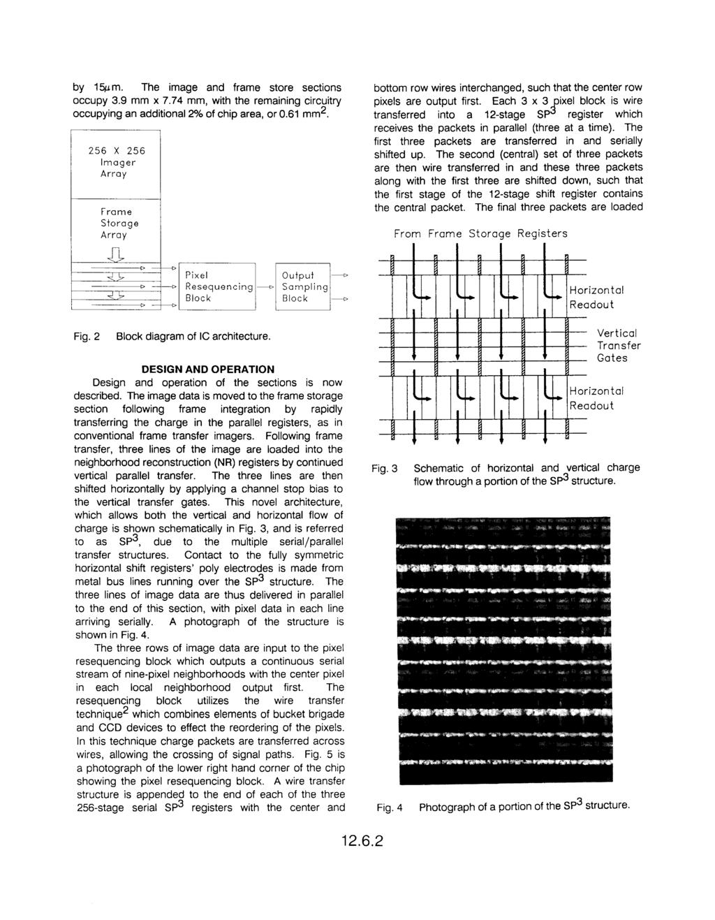
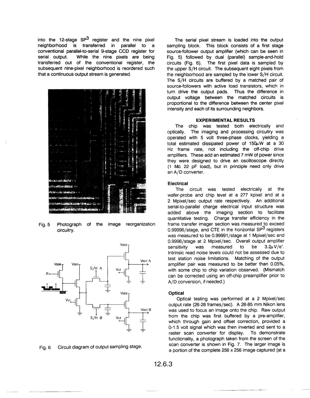
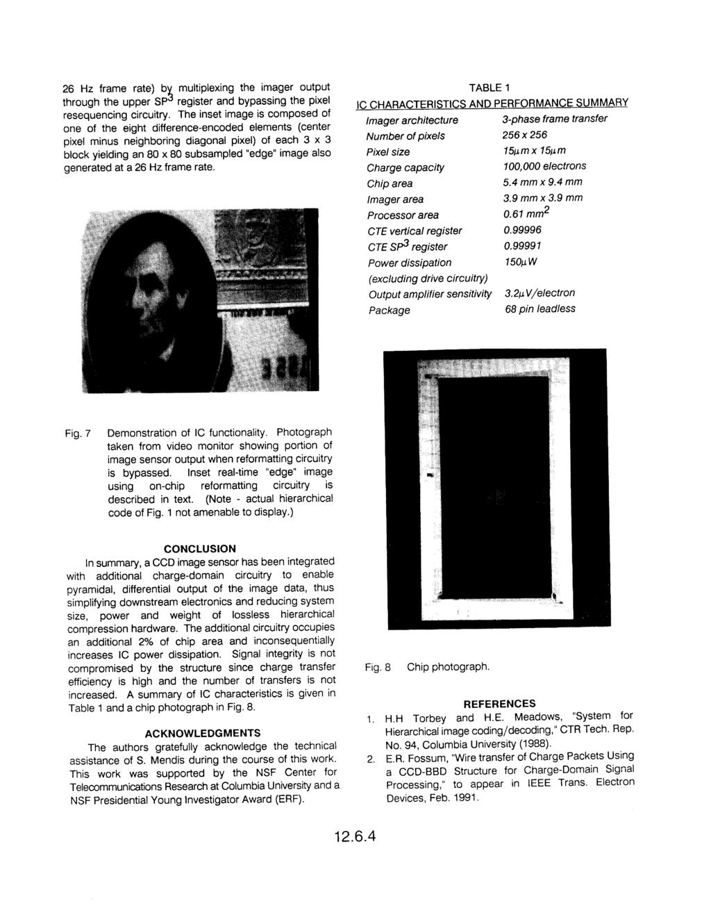
5 IMPROVED SCAN OF FIGURES 01/2009 into the 12-stage SP 3 register and the nine pixel neighborhood is transferred in parallel to a conventional parallel-to-serial 9-stage CCD register for serial output. While the nine pixels are being transferred out of the conventional register, the subsequent nine-pixel neighborhood is reordered such that a continuous output stream is generated. The serial pixel stream is loaded into the output sampling block. This block consists of a first stage source-follower output amplifier (which can be seen in Fig. 5) followed by dual (parallel) sample-and-hold circuits (Fig. 6). The first pixel data is sampled by the upper S/H circuit. The subsequent eight pixels from the neighborhood are sampled by the lower S/H circuit. The S/H circuits are buffered by a matched pair of source-followers with active load transistors, which in turn drive the output pads. Thus the difference in output voltage between the matched circuits is proportional to the difference between the center pixel intensity and each of its surrounding neighbors. EXPERIMENTAL RESULTS The chip was tested both electrically and optically. The imaging and processing circuitry was operated with 5 volt three-phase clocks, yielding a total estimated dissipated power of 150JL W at a 30 Hz frame rate, not including the off-chip drive amplifiers. These add an estimated 7 mw of power since they were designed to drive an oscilloscope directly (1 rvtn 22 pf load), but in principle need only drive an A/D converter. Fig. 5 photograph of the image reorganization circuitry. R VOD1 -.L S/H A Electrical The circuit was tested electrically at the wafer-probe and chip level at a 277 kpixel and at a 2 Mpixel/sec output rate respectively. An additional serial-to-parallel charge electrical input structure was added above the imaging section to facilitate quantitative testing. Charge transfer efficiency in the frame transfer imager section was measured to exceed /stage, and CTE in the horizontal Sp3 registers was measured to be /stage at 1 Mpixel/sec and /stage at 2 Mpixeljsec. Overall output amplifier sensitivity was measured to be 3.2j.J.V/e-. Intrinsic read noise levels could not be assessed due to test station noise limitations. Matching of the output amplifier pair was measured to be better than 0.05%, with some chip to chip variation observed. (Mismatch can be corrected using an off-chip preamplifier prior to A/D conversion, if needed.) Fig. 6 Circuit diagram of output sampling stage. Optical Optical testing was performed at a 2 Mpixeljsec output rate (26-28 frames/sec). A mm Nikon lens was used to focus an image onto the chip. Raw output from the chip was first buffered by a pre-amplifier, which through gain and offset correction, provided a volt signal which was then inverted and sent to a raster scan converter for display. To demonstrate functionality, a photograph taken from the screen of the scan converter is shown in Fig. 7. The larger image is a portion of the complete 256 x 256 image captured (at a
 of each 3 x 3 block yielding an 80 x 80 subsampled \"edge\" image also")
6 IMPROVED SCAN OF FIGURES 01/ Hz frame rate) b~ multiplexing the imager output through the upper SP register and bypassing the pixel resequencing circuitry. The inset image is composed of one of the eight difference-encoded elements (center pixel minus neighboring diagonal pixel) of each 3 x 3 block yielding an 80 x 80 subsampled "edge" image also generated at a 26 Hz frame rate. TABLE 1 IC CHARACTERISTICS AND PERFORMANCE SUMMARY Imagerarchftecture Number of pixels Pixel size Charge capacity Chip area Imager area Processor area CTE vertical register CTE sp3 register Power dissipation (excluding drive circuitry) Output amplifier sensitivity Package 3-phase frame transfer 256x J.Lm x 15J.Lm 100,000 electrons 5.4 mm x 9.4 mm 3.9 mm x 3.9 mm 0.61 mm J.LW 3.2J.L Vlelectron 68 pin leadless Fig. 7 Demonstration of IC functionality. Photograph taken from video monitor showing portion of image sensor output when reformatting circuitry is bypassed. Inset real-time "edge" image using on-chip reformatting circuitry is described in text. (Note - actual hierarchical code of Fig. 1 not amenable to display.) CONCLUSION In summary, a CCD image sensor has been integrated with additional charge-domain circuitry to enable pyramidal, differential output of the image data, thus simplifying downstream electronics and reducing system size, power and weight of lossless hierarchical compression hardware. The additional circuitry occupies an additional 2"'{' of chip area and inconsequentially increases IC power dissipation. Signal integrity is not compromised by the structure since charge transfer efficiency is high and the number of transfers is not increased. A summary of IC characteristics is given in Table 1 and a chip photograph in Fig. 8. ACKNOWLEDGMENTS The authors gratefully acknowledge the technical assistance of S. Mendis during the course of this work. This work was supported by the NSF Center for Teleoommunications Research at Columbia University and a NSF Presidential Young Investigator Award (ERF). Fig. 8 Chip photograph. REFERENCES 1. H.H Torbey and H.E. Meadows, "System for Hierarchical image codingjdeooding," CTR Tech. Rep. No. 94, Columbia University (1988). 2. E.R. Fossum, "Wire transfer of Charge Packets Using a CCD-BBD Structure for Charge-Domain Signal Processing," to appear in IEEE Trans. Electron Devices, Feb
Chapter 9 MSI Logic Circuits
 Chapter 9 MSI Logic Circuits Chapter 9 Objectives Selected areas covered in this chapter: Analyzing/using decoders & encoders in circuits. Advantages and disadvantages of LEDs and LCDs. Observation/analysis
Dual Link DVI Receiver Implementation
 Dual Link DVI Receiver Implementation This application note describes some features of single link receivers that must be considered when using 2 devices for a dual link application. Specific characteristics
A video signal processor for motioncompensated field-rate upconversion in consumer television
 A video signal processor for motioncompensated field-rate upconversion in consumer television B. De Loore, P. Lippens, P. Eeckhout, H. Huijgen, A. Löning, B. McSweeney, M. Verstraelen, B. Pham, G. de Haan,
HDMI 1.3 Demystified
 October 5, 2006 HDMI 1.3 Demystified Xiaozheng Lu, Senior Vice President, Product Development, AudioQuest The release of the new HDMI 1.3 specification on 6/22/2006 created both excitement and confusion
CCD Element Linear Image Sensor CCD Element Line Scan Image Sensor
 1024-Element Linear Image Sensor CCD 134 1024-Element Line Scan Image Sensor FEATURES 1024 x 1 photosite array 13µm x 13µm photosites on 13µm pitch Anti-blooming and integration control Enhanced spectral
Display Interfaces. Display solutions from Inforce. MIPI-DSI to Parallel RGB format
 Display Interfaces Snapdragon processors natively support a few popular graphical displays like MIPI-DSI/LVDS and HDMI or a combination of these. HDMI displays that output any of the standard resolutions
WE MUST BE MAD Pushing FIERA to its Limits
 WE MUST BE MAD Pushing FIERA to its Limits Roland Reiss, Andrea Balestra, Claudio Cumani, Christoph Geimer, Javier Reyes, Enrico Marchetti, Joana Santos European Southern Observatory, Karl-Schwarzschild-Str.
Motion Video Compression
 7 Motion Video Compression 7.1 Motion video Motion video contains massive amounts of redundant information. This is because each image has redundant information and also because there are very few changes
PICOSECOND TIMING USING FAST ANALOG SAMPLING
 PICOSECOND TIMING USING FAST ANALOG SAMPLING H. Frisch, J-F Genat, F. Tang, EFI Chicago, Tuesday 6 th Nov 2007 INTRODUCTION In the context of picosecond timing, analog detector pulse sampling in the 10
Reading an Image using CMOS Linear Image Sensor. S.R.Shinthu 1, P.Maheswari 2, C.S.Manikandababu 3. 1 Introduction. A.
 International Journal of Inventions in Computer Science and Engineering, Volume 2 Issue 4 April 2015 Reading an Image using CMOS Linear Image Sensor S.R.Shinthu 1, P.Maheswari 2, C.S.Manikandababu 3 1,2
Lossless Compression Algorithms for Direct- Write Lithography Systems
 Lossless Compression Algorithms for Direct- Write Lithography Systems Hsin-I Liu Video and Image Processing Lab Department of Electrical Engineering and Computer Science University of California at Berkeley
CCD220 Back Illuminated L3Vision Sensor Electron Multiplying Adaptive Optics CCD
 CCD220 Back Illuminated L3Vision Sensor Electron Multiplying Adaptive Optics CCD FEATURES 240 x 240 pixel image area 24 µm square pixels Split frame transfer 100% fill factor Back-illuminated for high
UNIT V 8051 Microcontroller based Systems Design
 UNIT V 8051 Microcontroller based Systems Design INTERFACING TO ALPHANUMERIC DISPLAYS Many microprocessor-controlled instruments and machines need to display letters of the alphabet and numbers. Light
Dual Link DVI Receiver Implementation
 Dual Link DVI Receiver Implementation This application note describes some features of single link receivers that must be considered when using 2 devices for a dual link application. Specific characteristics
MAX11503 BUFFER. Σ +6dB BUFFER GND *REMOVE AND SHORT FOR DC-COUPLED OPERATION
 19-4031; Rev 0; 2/08 General Description The is a low-power video amplifier with a Y/C summer and chroma mute. The device accepts an S-video or Y/C input and sums the luma (Y) and chroma (C) signals into
Chapter 2. Digital Circuits
 Chapter 2. Digital Circuits Logic gates Flip-flops FF registers IC registers Data bus Encoders/Decoders Multiplexers Troubleshooting digital circuits Most contents of this chapter were covered in 88-217
Technology Scaling Issues of an I DDQ Built-In Current Sensor
 Technology Scaling Issues of an I DDQ Built-In Current Sensor Bin Xue, D. M. H. Walker Dept. of Computer Science Texas A&M University College Station TX 77843-3112 Tel: (979) 862-4387 Email: {binxue, walker}@cs.tamu.edu
A FOUR GAIN READOUT INTEGRATED CIRCUIT : FRIC 96_1
 A FOUR GAIN READOUT INTEGRATED CIRCUIT : FRIC 96_1 J. M. Bussat 1, G. Bohner 1, O. Rossetto 2, D. Dzahini 2, J. Lecoq 1, J. Pouxe 2, J. Colas 1, (1) L. A. P. P. Annecy-le-vieux, France (2) I. S. N. Grenoble,
Logic Devices for Interfacing, The 8085 MPU Lecture 4
 Logic Devices for Interfacing, The 8085 MPU Lecture 4 1 Logic Devices for Interfacing Tri-State devices Buffer Bidirectional Buffer Decoder Encoder D Flip Flop :Latch and Clocked 2 Tri-state Logic Outputs
A MISSILE INSTRUMENTATION ENCODER
 A MISSILE INSTRUMENTATION ENCODER Item Type text; Proceedings Authors CONN, RAYMOND; BREEDLOVE, PHILLIP Publisher International Foundation for Telemetering Journal International Telemetering Conference
RX40_V1_0 Measurement Report F.Faccio
 RX40_V1_0 Measurement Report F.Faccio This document follows the previous report An 80Mbit/s Optical Receiver for the CMS digital optical link, dating back to January 2000 and concerning the first prototype
Laboratory 9 Digital Circuits: Flip Flops, One-Shot, Shift Register, Ripple Counter
 page 1 of 5 Digital Circuits: Flip Flops, One-Shot, Shift Register, Ripple Counter Introduction In this lab, you will learn about the behavior of the D flip-flop, by employing it in 3 classic circuits:
WINTER 15 EXAMINATION Model Answer
 Important Instructions to examiners: 1) The answers should be examined by key words and not as word-to-word as given in the model answer scheme. 2) The model answer and the answer written by candidate
CCD Datasheet Electron Multiplying CCD Sensor Back Illuminated, 1024 x 1024 Pixels 2-Phase IMO
 CCD351-00 Datasheet Electron Multiplying CCD Sensor Back Illuminated, 1024 x 1024 Pixels 2-Phase IMO MAIN FEATURES 1024 x 1024 active pixels 10µm square pixels Variable multiplicative gain Frame rates
CCD 143A 2048-Element High Speed Linear Image Sensor
 A CCD 143A 2048-Element High Speed Linear Image Sensor FEATURES 2048 x 1 photosite array 13µm x 13µm photosites on 13µm pitch High speed = up to 20MHz data rates Enhanced spectral response Low dark signal
A High-Speed CMOS Image Sensor with Column-Parallel Single Capacitor CDSs and Single-slope ADCs
 A High-Speed CMOS Image Sensor with Column-Parallel Single Capacitor CDSs and Single-slope ADCs LI Quanliang, SHI Cong, and WU Nanjian (The State Key Laboratory for Superlattices and Microstructures, Institute
EXPERIMENT #6 DIGITAL BASICS
 EXPERIMENT #6 DIGITL SICS Digital electronics is based on the binary number system. Instead of having signals which can vary continuously as in analog circuits, digital signals are characterized by only
SMPTE STANDARD Gb/s Signal/Data Serial Interface. Proposed SMPTE Standard for Television SMPTE 424M Date: < > TP Rev 0
 Proposed SMPTE Standard for Television Date: TP Rev 0 SMPTE 424M-2005 SMPTE Technology Committee N 26 on File Management and Networking Technology SMPTE STANDARD- --- 3 Gb/s Signal/Data Serial
Light Emitting Diodes and Digital Circuits I
 LED s and Digital Circuits I. p. 1 Light Emitting Diodes and Digital Circuits I The Light Emitting Diode: The light emitting diode (LED) is used as a probe in the digital experiments below. We begin by
Simple Combination Lock Circuit Project. Johnathan Sam
 Simple Combination Lock Circuit Project Johnathan Sam Engr 210 5/16/2013 Bill Of Materials Resistors R1-5 Resistor 47 KOhm 1/4 Watt 5% Carbon Film R6 Resistor 4.7 KOhm 1/4 Watt 5% Carbon Film Transistors
Computer Systems Architecture
 Computer Systems Architecture Fundamentals Of Digital Logic 1 Our Goal Understand Fundamentals and basics Concepts How computers work at the lowest level Avoid whenever possible Complexity Implementation
MULTIDYNE INNOVATIONS IN TELEVISION TESTING & DISTRIBUTION DIGITAL VIDEO, AUDIO & DATA FIBER OPTIC MULTIPLEXER TRANSPORT SYSTEM
 MULTIDYNE INNOVATIONS IN TELEVISION TESTING & DISTRIBUTION INSTRUCTION MANUAL DVM-1000 DIGITAL VIDEO, AUDIO & DATA FIBER OPTIC MULTIPLEXER TRANSPORT SYSTEM MULTIDYNE Electronics, Inc. Innovations in Television
Converters: Analogue to Digital
 Converters: Analogue to Digital Presented by: Dr. Walid Ghoneim References: Process Control Instrumentation Technology, Curtis Johnson Op Amps Design, Operation and Troubleshooting. David Terrell 1 - ADC
T ips in measuring and reducing monitor jitter
 APPLICAT ION NOT E T ips in measuring and reducing Philips Semiconductors Abstract The image jitter and OSD jitter are mentioned in this application note. Jitter measuring instruction is also included.
Simulation Mismatches Can Foul Up Test-Pattern Verification
 1 of 5 12/17/2009 2:59 PM Technologies Design Hotspots Resources Shows Magazine ebooks & Whitepapers Jobs More... Click to view this week's ad screen [ D e s i g n V i e w / D e s i g n S o lu ti o n ]
SMPTE x720 Progressive Image Sample Structure - Analog and Digital representation and Analog Interface
 MISB RP 0403.1 Recommended Practice Digital Representation and Source Interface formats for Infrared Motion Imagery mapped into 1280 x 720 format Bit-Serial Digital Interface 01 February 2010 1 Scope The
MSO-28 Oscilloscope, Logic Analyzer, Spectrum Analyzer
 Link Instruments Innovative Test & Measurement solutions since 1986 Store Support Oscilloscopes Logic Analyzers Pattern Generators Accessories MSO-28 Oscilloscope, Logic Analyzer, Spectrum Analyzer $ The
IEEE Santa Clara ComSoc/CAS Weekend Workshop Event-based analog sensing
 IEEE Santa Clara ComSoc/CAS Weekend Workshop Event-based analog sensing Theodore Yu theodore.yu@ti.com Texas Instruments Kilby Labs, Silicon Valley Labs September 29, 2012 1 Living in an analog world The
Complete 10-Bit, 25 MHz CCD Signal Processor AD9943
 a FEATURES 25 MSPS Correlated Double Sampler (CDS) 6 db to 40 db 10-Bit Variable Gain Amplifier (VGA) Low Noise Optical Black Clamp Circuit Preblanking Function 10-Bit, 25 MSPS A/D Converter No Missing
Introduction to Data Conversion and Processing
 Introduction to Data Conversion and Processing The proliferation of digital computing and signal processing in electronic systems is often described as "the world is becoming more digital every day." Compared
VLSI Design: 3) Explain the various MOSFET Capacitances & their significance. 4) Draw a CMOS Inverter. Explain its transfer characteristics
 Explain the various MOSFET Capacitances & their significance. 4) Draw a CMOS Inverter. Explain its transfer characteristics") 1) Explain why & how a MOSFET works VLSI Design: 2) Draw Vds-Ids curve for a MOSFET. Now, show how this curve changes (a) with increasing Vgs (b) with increasing transistor width (c) considering Channel
1) Explain why & how a MOSFET works VLSI Design: 2) Draw Vds-Ids curve for a MOSFET. Now, show how this curve changes (a) with increasing Vgs (b) with increasing transistor width (c) considering Channel
A BBD replacement and adjustment procedure
 A-188-1 BBD replacement and adjustment procedure The following steps have to be carried out with the unpowered A-188-1 module (i.e. the module is not connected to the A-100 bus board or the module is connected
8 DIGITAL SIGNAL PROCESSOR IN OPTICAL TOMOGRAPHY SYSTEM
 Recent Development in Instrumentation System 99 8 DIGITAL SIGNAL PROCESSOR IN OPTICAL TOMOGRAPHY SYSTEM Siti Zarina Mohd Muji Ruzairi Abdul Rahim Chiam Kok Thiam 8.1 INTRODUCTION Optical tomography involves
Cryoelectronics. MS-FLL User s Manual. Mr. SQUID Flux-Locked Loop. STAR Cryoelectronics 25 Bisbee Court, Suite A Santa Fe, NM U. S. A.
 Cryoelectronics MS-FLL User s Manual Mr. SQUID Flux-Locked Loop STAR Cryoelectronics 25 Bisbee Court, Suite A Santa Fe, NM 87508 U. S. A. STAR Cryoelectronics, LLC ii Table of Contents Revision Record...
Complete 10-Bit/12-Bit, 25 MHz CCD Signal Processor AD9943/AD9944
 a FEATURES 25 MSPS Correlated Double Sampler (CDS) 6 db to 40 db 10-Bit Variable Gain Amplifier (VGA) Low Noise Optical Black Clamp Circuit Preblanking Function 10-Bit (AD9943), 12-Bit (AD9944), 25 MSPS
Interframe Bus Encoding Technique for Low Power Video Compression
 Interframe Bus Encoding Technique for Low Power Video Compression Asral Bahari, Tughrul Arslan and Ahmet T. Erdogan School of Engineering and Electronics, University of Edinburgh United Kingdom Email:
Build A Video Switcher
 Build A Video Switcher VIDEOSISTEMAS serviciotecnico@videosistemas.com www.videosistemas.com Reprinted with permission from Electronics Now Magazine September 1997 issue Copyright Gernsback Publications,
VHDL Design and Implementation of FPGA Based Logic Analyzer: Work in Progress
 VHDL Design and Implementation of FPGA Based Logic Analyzer: Work in Progress Nor Zaidi Haron Ayer Keroh +606-5552086 zaidi@utem.edu.my Masrullizam Mat Ibrahim Ayer Keroh +606-5552081 masrullizam@utem.edu.my
ECEN689: Special Topics in High-Speed Links Circuits and Systems Spring 2011
 ECEN689: Special Topics in High-Speed Links Circuits and Systems Spring 2011 Lecture 9: TX Multiplexer Circuits Sam Palermo Analog & Mixed-Signal Center Texas A&M University Announcements & Agenda Next
ISSCC 2006 / SESSION 14 / BASEBAND AND CHANNEL PROCESSING / 14.6
 ISSCC 2006 / SESSION 14 / BASEBAND AND CHANNEL PROSSING / 14.6 14.6 A 1.8V 250mW COFDM Baseband Receiver for DVB-T/H Applications Lei-Fone Chen, Yuan Chen, Lu-Chung Chien, Ying-Hao Ma, Chia-Hao Lee, Yu-Wei
Light Emitting Diodes and Digital Circuits I
 LED s and Digital Circuits I. p. 1 Light Emitting Diodes and Digital Circuits I Tasks marked by an asterisk (*) may be carried out before coming to the lab. The Light Emitting Diode: The light emitting
Application Note. Introduction of JDI MIP reflective type color LCD
 April, 2016 Application Note Introduction of JDI MIP reflective type color Introduction JDI releases a series of MIP (memory in pixel) reflective type color s which realize high reflectance performance
Troubleshooting EMI in Embedded Designs White Paper
 Troubleshooting EMI in Embedded Designs White Paper Abstract Today, engineers need reliable information fast, and to ensure compliance with regulations for electromagnetic compatibility in the most economical
AND9191/D. KAI-2093 Image Sensor and the SMPTE Standard APPLICATION NOTE.
 KAI-09 Image Sensor and the SMPTE Standard APPLICATION NOTE Introduction The KAI 09 image sensor is designed to provide HDTV resolution video at 0 fps in a progressive scan mode. In this mode, the sensor
1ms Column Parallel Vision System and It's Application of High Speed Target Tracking
 Proceedings of the 2(X)0 IEEE International Conference on Robotics & Automation San Francisco, CA April 2000 1ms Column Parallel Vision System and It's Application of High Speed Target Tracking Y. Nakabo,
LED7706/7/8. LED drivers for backlighting and lighting applications.
 LED7706/7/8 LED drivers for backlighting and lighting applications www.st.com/led Content Advanced power management to drive LEDs...3 LED7706/7: six rows of up to 10 white LEDs, with adjustable maximum
DIGITAL TECHNICS. Dr. Bálint Pődör. Óbuda University, Microelectronics and Technology Institute
 DIGITL TECHNICS Dr. álint Pődör Óbuda University, Microelectronics and Technology Institute 10. LECTURE (LOGIC CIRCUITS, PRT 2): MOS DIGITL CIRCUITS II 2016/2017 10. LECTURE: MOS DIGITL CIRCUITS II 1.
Light Emitting Diodes and Digital Circuits I
 LED s and Digital Circuits I. p. 1 Light Emitting Diodes and Digital Circuits I Tasks marked by an asterisk (*) may be carried out before coming to the lab. The Light Emitting Diode: The light emitting
Microbolometer based infrared cameras PYROVIEW with Fast Ethernet interface
 DIAS Infrared GmbH Publications No. 19 1 Microbolometer based infrared cameras PYROVIEW with Fast Ethernet interface Uwe Hoffmann 1, Stephan Böhmer 2, Helmut Budzier 1,2, Thomas Reichardt 1, Jens Vollheim
Bell. Program of Study. Accelerated Digital Electronics. Dave Bell TJHSST
 Program of Study Accelerated Digital Electronics TJHSST Dave Bell Course Selection Guide Description: Students learn the basics of digital electronics technology as they engineer a complex electronic system.
INDIAN INSTITUTE OF TECHNOLOGY KHARAGPUR NPTEL ONLINE CERTIFICATION COURSE. On Industrial Automation and Control
 INDIAN INSTITUTE OF TECHNOLOGY KHARAGPUR NPTEL ONLINE CERTIFICATION COURSE On Industrial Automation and Control By Prof. S. Mukhopadhyay Department of Electrical Engineering IIT Kharagpur Topic Lecture
16-BIT LOAD CELL/DUAL STATUS INPUT
 16-BIT LOAD CELL/DUAL STATUS INPUT On-board Excitation. +5VDC, (120mA). State-of-the-art Electromagnetic Noise Suppression Circuitry. Ensures signal integrity even in harsh EMC environments. Optional Excitation
QRF5000 MDU ENCODER. Data Sheet
 Radiant Communications Corporation 5001 Hadley Road South Plainfield NJ 07080 Tel (908) 757-7444 Fax (908) 757-8666 WWW.RCCFIBER.COM QRF5000 MDU ENCODER Data Sheet Version 1.1 1 Caution Verify proper grounding
Complete 12-Bit 40 MHz CCD Signal Processor AD9945
 Complete 12-Bit 40 MHz CCD Signal Processor AD9945 FEATURES 40 MSPS Correlated Double Sampler (CDS) 6 db to 40 db 10-Bit Variable Gain Amplifier (VGA) Low Noise Optical Black Clamp Circuit Preblanking
V6118 EM MICROELECTRONIC - MARIN SA. 2, 4 and 8 Mutiplex LCD Driver
 EM MICROELECTRONIC - MARIN SA 2, 4 and 8 Mutiplex LCD Driver Description The is a universal low multiplex LCD driver. The version 2 drives two ways multiplex (two blackplanes) LCD, the version 4, four
HMC814LC3B FREQ. MULTIPLIERS - ACTIVE - SMT. SMT GaAs MMIC x2 ACTIVE FREQUENCY MULTIPLIER, GHz OUTPUT. Features. Typical Applications
 Typical Applications The is ideal for: Clock Generation Applications: SONET OC-192 & SDH STM-64 Point-to-Point & VSAT Radios Test Instrumentation Military & Space Sensors Functional Diagram Features High
TYPICAL QUESTIONS & ANSWERS
 DIGITALS ELECTRONICS TYPICAL QUESTIONS & ANSWERS OBJECTIVE TYPE QUESTIONS Each Question carries 2 marks. Choose correct or the best alternative in the following: Q.1 The NAND gate output will be low if
Part 1: Introduction to computer graphics 1. Describe Each of the following: a. Computer Graphics. b. Computer Graphics API. c. CG s can be used in
 Part 1: Introduction to computer graphics 1. Describe Each of the following: a. Computer Graphics. b. Computer Graphics API. c. CG s can be used in solving Problems. d. Graphics Pipeline. e. Video Memory.
The Alice Silicon Pixel Detector (SPD) Peter Chochula for the Alice Pixel Collaboration
 Peter Chochula for the Alice Pixel Collaboration") The Alice Silicon Pixel Detector (SPD) Peter Chochula for the Alice Pixel Collaboration The Alice Pixel Detector R 1 =3.9 cm R 2 =7.6 cm Main Physics Goal Heavy Flavour Physics D 0 K π+ 15 days Pb-Pb data
The Alice Silicon Pixel Detector (SPD) Peter Chochula for the Alice Pixel Collaboration The Alice Pixel Detector R 1 =3.9 cm R 2 =7.6 cm Main Physics Goal Heavy Flavour Physics D 0 K π+ 15 days Pb-Pb data
Screen investigations for low energetic electron beams at PITZ
 1 Screen investigations for low energetic electron beams at PITZ S. Rimjaem, J. Bähr, H.J. Grabosch, M. Groß Contents Review of PITZ setup Screens and beam profile monitors at PITZ Test results Summary
ELECTRICAL ENGINEERING DEPARTMENT California Polytechnic State University
 EECTRICA ENGINEERING DEPARTMENT California Polytechnic State University EE 361 NAND ogic Gate, RS Flip-Flop & JK Flip-Flop Pre-lab 7 1. Draw the logic symbol and construct the truth table for a NAND gate.
THE STRUCTURE AND ADVANTAGES OF DIGITAL TRAINING SET FOR COMPUTER ENGINEERING
 THE STRUCTURE AND ADVANTAGES OF DIGITAL TRAINING SET FOR COMPUTER ENGINEERING GÜLAY TEZEL ŞİRZAT KAHRAMANLI Department Of Computer Engineering Selçuk University Department Of Computer Engineering, Faculty
MODULAR DIGITAL ELECTRONICS TRAINING SYSTEM
 MODULAR DIGITAL ELECTRONICS TRAINING SYSTEM MDETS UCTECH's Modular Digital Electronics Training System is a modular course covering the fundamentals, concepts, theory and applications of digital electronics.
Chapter 1 HDMI-FMC Development Kit Chapter 2 Introduction of the HDMI-FMC Card Chapter 3 Using the HDMI-FMC Board...
 Chapter 1 HDMI-FMC Development Kit... 2 1-1 Package Contents... 3 1-2 HDMI-FMC System CD... 3 1-3 Getting Help... 3 Chapter 2 Introduction of the HDMI-FMC Card... 4 2-1 Features... 5 2-2 Block Diagram
FDTD_SPICE Analysis of EMI and SSO of LSI ICs Using a Full Chip Macro Model
 FDTD_SPICE Analysis of EMI and SSO of LSI ICs Using a Full Chip Macro Model Norio Matsui Applied Simulation Technology 2025 Gateway Place #318 San Jose, CA USA 95110 matsui@apsimtech.com Neven Orhanovic
IC Design of a New Decision Device for Analog Viterbi Decoder
 IC Design of a New Decision Device for Analog Viterbi Decoder Wen-Ta Lee, Ming-Jlun Liu, Yuh-Shyan Hwang and Jiann-Jong Chen Institute of Computer and Communication, National Taipei University of Technology
AD9884A Evaluation Kit Documentation
 a (centimeters) AD9884A Evaluation Kit Documentation Includes Documentation for: - AD9884A Evaluation Board - SXGA Panel Driver Board Rev 0 1/4/2000 Evaluation Board Documentation For the AD9884A Purpose
RECOMMENDATION ITU-R BT.1201 * Extremely high resolution imagery
 Rec. ITU-R BT.1201 1 RECOMMENDATION ITU-R BT.1201 * Extremely high resolution imagery (Question ITU-R 226/11) (1995) The ITU Radiocommunication Assembly, considering a) that extremely high resolution imagery
DESIGN PHILOSOPHY We had a Dream...
 DESIGN PHILOSOPHY We had a Dream... The from-ground-up new architecture is the result of multiple prototype generations over the last two years where the experience of digital and analog algorithms and
How to overcome/avoid High Frequency Effects on Debug Interfaces Trace Port Design Guidelines
 How to overcome/avoid High Frequency Effects on Debug Interfaces Trace Port Design Guidelines An On-Chip Debugger/Analyzer (OCD) like isystem s ic5000 (Figure 1) acts as a link to the target hardware by
Digital Audio Design Validation and Debugging Using PGY-I2C
 Digital Audio Design Validation and Debugging Using PGY-I2C Debug the toughest I 2 S challenges, from Protocol Layer to PHY Layer to Audio Content Introduction Today s digital systems from the Digital
Brief Description of Circuit Functions. The brief ckt. description of V20 107E5 17 Monitor
 Exhibit 4 Brief Description of Circuit Functions The brief ckt. description of V20 107E5 17 Monitor 0. Functional Block Diagram 1. General Description 2. Description of Circuit Diagram A. Power Supply
DESIGN AND ANALYSIS OF COMBINATIONAL CODING CIRCUITS USING ADIABATIC LOGIC
 DESIGN AND ANALYSIS OF COMBINATIONAL CODING CIRCUITS USING ADIABATIC LOGIC ARCHITA SRIVASTAVA Integrated B.tech(ECE) M.tech(VLSI) Scholar, Jayoti Vidyapeeth Women s University, Rajasthan, India, Email:
Brief Description of Circuit Functions
 Exhibit 4 Brief Description of Circuit Functions Function Description for Hudson4 190P5 1. General 190P5 is the newest generation of Hudson 19 TFT Flat Panel Display Monitor. It designed with hyper integrity,
Audio and Video II. Video signal +Color systems Motion estimation Video compression standards +H.261 +MPEG-1, MPEG-2, MPEG-4, MPEG- 7, and MPEG-21
 Audio and Video II Video signal +Color systems Motion estimation Video compression standards +H.261 +MPEG-1, MPEG-2, MPEG-4, MPEG- 7, and MPEG-21 1 Video signal Video camera scans the image by following
IT T35 Digital system desigm y - ii /s - iii
 UNIT - III Sequential Logic I Sequential circuits: latches flip flops analysis of clocked sequential circuits state reduction and assignments Registers and Counters: Registers shift registers ripple counters
Electrical and Electronic Laboratory Faculty of Engineering Chulalongkorn University. Cathode-Ray Oscilloscope (CRO)
") 2141274 Electrical and Electronic Laboratory Faculty of Engineering Chulalongkorn University Cathode-Ray Oscilloscope (CRO) Objectives You will be able to use an oscilloscope to measure voltage, frequency
2141274 Electrical and Electronic Laboratory Faculty of Engineering Chulalongkorn University Cathode-Ray Oscilloscope (CRO) Objectives You will be able to use an oscilloscope to measure voltage, frequency
The Multistandard Full Hd Video-Codec Engine On Low Power Devices
 The Multistandard Full Hd Video-Codec Engine On Low Power Devices B.Susma (M. Tech). Embedded Systems. Aurora s Technological & Research Institute. Hyderabad. B.Srinivas Asst. professor. ECE, Aurora s
P.Akila 1. P a g e 60
 Designing Clock System Using Power Optimization Techniques in Flipflop P.Akila 1 Assistant Professor-I 2 Department of Electronics and Communication Engineering PSR Rengasamy college of engineering for
Scan. This is a sample of the first 15 pages of the Scan chapter.
 Scan This is a sample of the first 15 pages of the Scan chapter. Note: The book is NOT Pinted in color. Objectives: This section provides: An overview of Scan An introduction to Test Sequences and Test
Challenges in the design of a RGB LED display for indoor applications
 Synthetic Metals 122 (2001) 215±219 Challenges in the design of a RGB LED display for indoor applications Francis Nguyen * Osram Opto Semiconductors, In neon Technologies Corporation, 19000, Homestead
AE/AC/AT54 LINEAR ICs & DIGITAL ELECTRONICS DEC 2014
 Q.2a. Give the classification of different IC technologies. IETE 1 b.for a differential amplifier using ideal op-amp(shown in Fig. 2) (i) Find the output voltage v o (ii) Show that the output corresponding
Integration of Virtual Instrumentation into a Compressed Electricity and Electronic Curriculum
 Integration of Virtual Instrumentation into a Compressed Electricity and Electronic Curriculum Arif Sirinterlikci Ohio Northern University Background Ohio Northern University Technological Studies Department
HIGH SPEED CLOCK DISTRIBUTION NETWORK USING CURRENT MODE DOUBLE EDGE TRIGGERED FLIP FLOP WITH ENABLE
 HIGH SPEED CLOCK DISTRIBUTION NETWORK USING CURRENT MODE DOUBLE EDGE TRIGGERED FLIP FLOP WITH ENABLE 1 Remil Anita.D, and 2 Jayasanthi.M, Karpagam College of Engineering, Coimbatore,India. Email: 1 :remiljobin92@gmail.com;
Checkpoint 2 Video Interface
 University of California at Berkeley College of Engineering Department of Electrical Engineering and Computer Sciences EECS150 Fall 1998 R. Fearing and Kevin Cho 1. Objective Checkpoint 2 Video Interface
Chapter 10 Basic Video Compression Techniques
 Chapter 10 Basic Video Compression Techniques 10.1 Introduction to Video compression 10.2 Video Compression with Motion Compensation 10.3 Video compression standard H.261 10.4 Video compression standard
ISSN Vol.08,Issue.24, December-2016, Pages:
 ISSN 2348 2370 Vol.08,Issue.24, December-2016, Pages:4666-4671 www.ijatir.org Design and Analysis of Shift Register using Pulse Triggered Latches N. NEELUFER 1, S. RAMANJI NAIK 2, B. SURESH BABU 3 1 PG
Viewing Serial Data on the Keysight Oscilloscopes
 Ming Hsieh Department of Electrical Engineering EE 109L - Introduction to Embedded Systems Viewing Serial Data on the Keysight Oscilloscopes by Allan G. Weber 1 Introduction The four-channel Keysight (ex-agilent)
Complete 12-Bit 40 MHz CCD Signal Processor AD9945
 Complete 12-Bit 40 MHz CCD Signal Processor AD9945 FEATURES 40 MSPS Correlated Double Sampler (CDS) 6 db to 40 db 10-Bit Variable Gain Amplifier (VGA) Low Noise Optical Black Clamp Circuit Preblanking
12-bit Wallace Tree Multiplier CMPEN 411 Final Report Matthew Poremba 5/1/2009
 12-bit Wallace Tree Multiplier CMPEN 411 Final Report Matthew Poremba 5/1/2009 Project Overview This project was originally titled Fast Fourier Transform Unit, but due to space and time constraints, the