EITF35: Introduction to Structured VLSI Design
|
|
|
- Jonah McCoy
- 6 years ago
- Views:
Transcription


1 EITF35: Introduction to Structured VLSI Design Part 4.2.1: Learn More Liang Liu 1
2 Outline Crossing clock domain Reset, synchronous or asynchronous? 2

3 Why two DFFs? 3

4 Crossing clock domain Multiple clock is needed in case: Inherent system requirement Different clocks for sampling and processing Chip size limitation Clock skew increases with the # FFs in a system Domain #1 Domain #2 4

5 Multiple Clocks: Problems We have been setting very strict rules to make our digital circuits safe: using a forbidden zone in both voltage and time dimensions Digital Values: distinguishing voltages representing 1 from 0 Digital Time: setup and hold time rules 5
6 Metastability With asynchronous inputs, we have to break the rules: we cannot guarantee that setup and hold time requirements are met at the inputs! What happens after timing violation? clk setup hold D Q? 6

7 Metastability in Digital Logic Metastability 7

8 Mechanical Metastability State A Launch a golf up a hill, 3 possible outcomes: Hit lightly: Rolls back Hit hard: Goes over Or: Stalls at the apex State A State B That last outcome is not stable: A gust of wind Brownian motion Can you tell the eventual state? 8
9 Metastability in Digital Logic Our hill is related to the VTC (Voltage Transfer Curve). The higher the gain thru the transition region The steeper the peak of the hill The harder to get into a metastable state. We can decrease the probability of getting into the metastable state, but we can t eliminate it 9
10 Metastability in Digital Logic Fixed clock edge Change the edge of inputs The input edge is moved in steps of 100ps and 1ps The behavior of outputs Three possible states Will exit metastability How long it takes to exit Metastability? 10
11 Exit Metastability Define a fixed-point voltage, V M, (always have) such that V IN = V M implies V OUT = V M Assume the device is sampling at some voltage V 0 near V M The time to settle to a stable value depends on (V 0 -V M ); its theoretically infinite for V 0 = V M 11
 The probability of remaining metastable at time T is Voltage Log(V-V M ) Time (ns)")
12 Exit Metastability The time to exit metastability depends logarithmically on (V 0 -V M ) The probability of remaining metastable at time T is Voltage Log(V-V M ) Time (ns) 12
13 MTBF: The probability of being metastable at time S? Two conditions have to be met concurrently An FF enters the metastable state An FF cannot resolve the metastable condition within S The rate of failure T W : time window around sampling edge incurring metastability F C : clock rate (assuming data change is uniformly distributed) F D : input change rate (input may not change every cycle) Mean time between failures (MTBF) 13
14 MTBF (Mean Time Between Failure) Let s calculate an ASIC for 28nm CMOS process τ: 10ps (different FFs have different τ) T W =20ps, F C =1GHz Data changes every ten clock cycles Allow 1 clock cycle to resolve metastability, S=T C MTBF= year! [For comparison: Age of oldest hominid fossil: 5x10 6 years Age of earth: 5x10 9 years] 14
15 The Two-Flip-Flop Synchronizer Asynchronous input FF1 FF2 Da D Q D Q Ds? CLK Synchronized signal Global low-skew clock S=T C 15
16 The Two-Flip-Flop Synchronizer Possible Outcomes 16
17 The Two-Flip-Flop Synchronizer Possible Outcomes Open Question: What is the limitation? 17
18 The Two-Flip-Flop Synchronizer Problems Just ensures that the receiving system does not enter a metastable state Not guarantee the function of the received signal Uncertainty Remains: Q2 goes high either one or two cycles later than the input D1 mush stay high for at least two cycles. How about data bus (multiple bits) crossing clock domain? Some bits may pass through the synchronizer after one cycle while others may take two cycles. 18
19 A Complete Synchronizer The sender place data on the bus The sender sends Req, Req gets synchronized by the top synchronization circuits The receiver gets data and sends back ACK Ack gets synchronized by the sender, and only then is the sender allowed to start a new cycle again. 19
20 FIFO FIFO (first in first out) Buffer Elastic storage between two subsystems 20

21 Circular FIFO How to Implement a FIFO? Circular queue implementation Use two pointers and a generic storage Write pointer: point to the empty slot before the head of the queue Read pointer: point to the tail of the queue 21
")
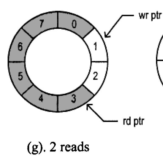
22 Circular FIFO (f)
23 FIFO Implementation Overall Architecture Storage Elements Reg. file FIFO Controller Read and write pointers: 2 counters Status circuit: full, empty 23
24 FIFO Implementation: Controller Augmented binary counter: Increase the counter by 1 bits Use LSBs for as register address Use MSB to distinguish full or empty

25 A Complete Synchronizer Control signals are synchronized, data pass through storage elements Assertion delay, it takes two clock cycles for the control signal passing through synchronizer Usually available in libraries The key question, how large the RAM should be? When in doubt, double it 25
26 Outline Crossing clock domain Reset, synchronous or asynchronous? 26
 should be resetable whether or not it is")

27 Reset Design Strategy Force the SoC into a known state for stable operations In general, every flip-flop in an SoC (ASIC) should be resetable whether or not it is required by the system Reset might be eliminated for high-performance pipeline FFs Many design issues must be considered before choosing a reset strategy for an ASIC design 27
28 General Coding Style: FFs Coding for synchronous and asynchronous reset architecture rtl of goodffstyle is signal q1 : std_logic; begin process (clk, rst_n) begin if (clk'event and clk = '1') then if (rst_n = '0') then q1 <= '0'; else q1 <= d; end if; end if; end process; end rtl; architecture rtl of goodffstyle is signal q1 : std_logic; begin process (clk) begin if (clk'event and clk = '1') then if (rst_n = '0') then q1 <= '0'; else q1 <= d; end if; end if; end process; end rtl; 28
29 Synchronous vs. Asynchronous Reset 29
30 Synchronous vs. Asynchronous Reset 80% designs using synchronous reset (investigation by Sunburst Design, Inc) we all know that the best way to do resets in an ASIC is to strictly use synchronous resets asynchronous resets are bad and should be avoided There are both advantages and disadvantages to using either synchronous or asynchronous resets. The designer must use an approach that is appropriate for the design. 30
31 Synchronous Reset reset is not part of the sensitivity list. reset is part of the input path 31
32 Synchronous Reset: one problem Synthesis tool may not easily distinguish the reset signal from any other data signal The synthesis tool could alternatively have produced the circuit If synthesis tool can distinguish reset, it will put reset as close to FFs as possible What If load=x Only a problem in simulation 32
33 Synchronous Reset Advantage Generally insure that the circuit is 100% synchronous. Will synthesize to smaller flip-flops Ensure that reset can only occur at an active clock edge. The clock works as a filter for small reset glitches. Disadvantage May need a pulse stretcher to guarantee a reset pulse width wide enough to ensure reset is present during an active edge of the clock Will require a clock in order to reset the circuit, e.g., if you have a gated clock to save power, the clock may be disabled 33
34 Asynchronous Reset reset is part of the sensitivity list. reset is not part of the input path 34

35 Asynchronous Reset Advantage The data path is guaranteed to be clean designs that are pushing the limit for data path timing, cannot afford to have added gates and additional net delays in the data path due to synchronous resets The most obvious advantage favoring asynchronous resets is that the circuit can be reset with or without a clock present Disadvantage If the asynchronous reset is released at or near the active clock edge of a flip-flop, the output of the flip-flop could go metastable and thus the reset state of the SoC could be lost. Spurious resets due to noise or glitches on the board or system reset 35

36 Reset Timing 36
37 Reset Removal Problem Reset recovery time: Time between when reset is de-asserted and the time that the clock signal goes high again. Synchronous reset, both the leading and trailing edges of the reset must be away from the active edge of the clock. 37 Active high reset
38 Reset Removal Problem Reset removal traversing different clock cycles Cause some registers or flip-flops to exit the reset state before others Reset Buffer Tree 38
39 Reset Removal Problem Reset removal traversing different clock cycles Cause some registers or flip-flops to exit the reset state before others Especially for high-rate clock and big chip Reset Buffer Tree 39 Active high reset
40 But Does it really matter? Single pipeline stage? After a few cycles, the entire pipeline will be operational Any incorrect data will be flushed out of the system In fact, there is little point in having a reset at all 40
41 But Does it really matter? Parallel pipeline Pipeline with feedback 41
42 Reset Synchronizer An external reset signal asynchronously resets a pair of master reset flip-flops, which in turn drive the master reset signal asynchronously Take advantage of the best of both asynchronous and synchronous reset styles. Takes two rising clock edges after reset removal to synchronize removal of the master reset. No metastability problems on the second flip-flop when reset is removed 42 Active low reset
43 Reset Glitch Filter Any input wide enough to meet the minimum reset pulse width for a flip-flop will cause the flip-flop to reset 43 Active low reset
44 Reset Glitch Filter Any input wide enough to meet the minimum reset pulse width for a flip-flop will cause the flip-flop to reset Delay line: Vendors provide a delay hard macro that can be hand instantiated Instantiate a slow buffer in a module 44 Active low reset
45 Xilinx Reset 45
 Has the same effect as a global reset It also initializes all RAM")
46 Xilinx Reset: covering 99.99% of cases Initialization after configuration (power-on reset) Has the same effect as a global reset It also initializes all RAM cells All program and data areas are defined even before the processor executes the first instruction 46
47 Xilinx Reset: Strategy for the 0.01% of Cases 47
48 Reference Readings Simulation and Synthesis Techniques for Asynchronous FIFO Design Synchronous Resets? Asynchronous Resets? I am so confused! How will I ever know which to use? Get Smart About Reset: Think Local, Not Global pers/wp272.pdf Get your Priorities Right Make your Design Up to 50% Smaller 48


49 Lecture No lecture tomorrow Sept. 28 th Monday ( ) Design for Test (DFT) Erik Larsson Associate Professor Sept. 29 th Tuesday ( ) Igor Tasevski 49
2.6 Reset Design Strategy
 2.6 Reset esign Strategy Many design issues must be considered before choosing a reset strategy for an ASIC design, such as whether to use synchronous or asynchronous resets, will every flipflop receive
Clock Domain Crossing. Presented by Abramov B. 1
 Clock Domain Crossing Presented by Abramov B. 1 Register Transfer Logic Logic R E G I S T E R Transfer Logic R E G I S T E R Presented by Abramov B. 2 RTL (cont) An RTL circuit is a digital circuit composed
EE178 Spring 2018 Lecture Module 5. Eric Crabill
 EE178 Spring 2018 Lecture Module 5 Eric Crabill Goals Considerations for synchronizing signals Clocks Resets Considerations for asynchronous inputs Methods for crossing clock domains Clocks The academic
https://daffy1108.wordpress.com/2014/06/08/synchronizers-for-asynchronous-signals/
 https://daffy1108.wordpress.com/2014/06/08/synchronizers-for-asynchronous-signals/ Synchronizers for Asynchronous Signals Asynchronous signals causes the big issue with clock domains, namely metastability.
EE178 Lecture Module 4. Eric Crabill SJSU / Xilinx Fall 2005
 EE178 Lecture Module 4 Eric Crabill SJSU / Xilinx Fall 2005 Lecture #9 Agenda Considerations for synchronizing signals. Clocks. Resets. Considerations for asynchronous inputs. Methods for crossing clock
EECS150 - Digital Design Lecture 10 - Interfacing. Recap and Topics
 EECS150 - Digital Design Lecture 10 - Interfacing Oct. 1, 2013 Prof. Ronald Fearing Electrical Engineering and Computer Sciences University of California, Berkeley (slides courtesy of Prof. John Wawrzynek)
Asynchronous & Synchronous Reset Design Techniques - Part Deux
 Clifford E. Cummings Don Mills Steve Golson Sunburst Design, Inc. LCDM Engineering Trilobyte Systems cliffc@sunburst-design.com mills@lcdm-eng.com sgolson@trilobyte.com ABSTRACT This paper will investigate
EE241 - Spring 2005 Advanced Digital Integrated Circuits
 EE241 - Spring 2005 Advanced Digital Integrated Circuits Lecture 21: Asynchronous Design Synchronization Clock Distribution Self-Timed Pipelined Datapath Req Ack HS Req Ack HS Req Ack HS Req Ack Start
Combinational vs Sequential
 Combinational vs Sequential inputs X Combinational Circuits outputs Z A combinational circuit: At any time, outputs depends only on inputs Changing inputs changes outputs No regard for previous inputs
More on Flip-Flops Digital Design and Computer Architecture: ARM Edition 2015 Chapter 3 <98> 98
 More on Flip-Flops Digital Design and Computer Architecture: ARM Edition 2015 Chapter 3 98 Review: Bit Storage SR latch S (set) Q R (reset) Level-sensitive SR latch S S1 C R R1 Q D C S R D latch Q
Sequencing. Lan-Da Van ( 范倫達 ), Ph. D. Department of Computer Science National Chiao Tung University Taiwan, R.O.C. Fall,
, Ph. D. Department of Computer Science National Chiao Tung University Taiwan, R.O.C. Fall,") Sequencing ( 范倫達 ), Ph. D. Department of Computer Science National Chiao Tung University Taiwan, R.O.C. Fall, 2013 ldvan@cs.nctu.edu.tw http://www.cs.nctu.edu.tw/~ldvan/ Outlines Introduction Sequencing
Sequencing ( 范倫達 ), Ph. D. Department of Computer Science National Chiao Tung University Taiwan, R.O.C. Fall, 2013 ldvan@cs.nctu.edu.tw http://www.cs.nctu.edu.tw/~ldvan/ Outlines Introduction Sequencing
cascading flip-flops for proper operation clock skew Hardware description languages and sequential logic
 equential logic equential circuits simple circuits with feedback latches edge-triggered flip-flops Timing methodologies cascading flip-flops for proper operation clock skew Basic registers shift registers
Glitches/hazards and how to avoid them. What to do when the state machine doesn t fit!
 State Machine Signaling Timing Behavior Glitches/hazards and how to avoid them SM Partitioning What to do when the state machine doesn t fit! State Machine Signaling Introducing Idle States (synchronous
IT T35 Digital system desigm y - ii /s - iii
 UNIT - III Sequential Logic I Sequential circuits: latches flip flops analysis of clocked sequential circuits state reduction and assignments Registers and Counters: Registers shift registers ripple counters
Objectives. Combinational logics Sequential logics Finite state machine Arithmetic circuits Datapath
 Objectives Combinational logics Sequential logics Finite state machine Arithmetic circuits Datapath In the previous chapters we have studied how to develop a specification from a given application, and
Sequential logic. Circuits with feedback. How to control feedback? Sequential circuits. Timing methodologies. Basic registers
 equential logic equential circuits simple circuits with feedback latches edge-triggered flip-flops Timing methodologies cascading flip-flops for proper operation clock skew Basic registers shift registers
Chapter 2 Clocks and Resets
 Chapter 2 Clocks and Resets 2.1 Introduction The cost of designing ASICs is increasing every year. In addition to the non-recurring engineering (NRE) and mask costs, development costs are increasing due
Outline. EECS150 - Digital Design Lecture 27 - Asynchronous Sequential Circuits. Cross-coupled NOR gates. Asynchronous State Transition Diagram
 EECS150 - Digital Design Lecture 27 - Asynchronous Sequential Circuits Nov 26, 2002 John Wawrzynek Outline SR Latches and other storage elements Synchronizers Figures from Digital Design, John F. Wakerly
Asynchronous inputs. 9 - Metastability and Clock Recovery. A simple synchronizer. Only one synchronizer per input
 9 - Metastability and Clock Recovery Asynchronous inputs We will consider a number of issues related to asynchronous inputs, multiple clock domains, clock synchronisation and clock distribution. Useful
Chapter 6. Flip-Flops and Simple Flip-Flop Applications
 Chapter 6 Flip-Flops and Simple Flip-Flop Applications Basic bistable element It is a circuit having two stable conditions (states). It can be used to store binary symbols. J. C. Huang, 2004 Digital Logic
Feedback Sequential Circuits
 Feedback Sequential Circuits sequential circuit output depends on 1. current inputs 2. past sequence of inputs current state feedback sequential circuit uses ordinary gates and feedback loops to create
Figure 1 shows a simple implementation of a clock switch, using an AND-OR type multiplexer logic.
 1. CLOCK MUXING: With more and more multi-frequency clocks being used in today's chips, especially in the communications field, it is often necessary to switch the source of a clock line while the chip
Sequential Circuit Design: Principle
 Sequential Circuit Design: Principle modified by L.Aamodt 1 Outline 1. 2. 3. 4. 5. 6. 7. 8. Overview on sequential circuits Synchronous circuits Danger of synthesizing asynchronous circuit Inference of
DEDICATED TO EMBEDDED SOLUTIONS
 DEDICATED TO EMBEDDED SOLUTIONS DESIGN SAFE FPGA INTERNAL CLOCK DOMAIN CROSSINGS ESPEN TALLAKSEN DATA RESPONS SCOPE Clock domain crossings (CDC) is probably the worst source for serious FPGA-bugs that
Digital Logic Design Sequential Circuits. Dr. Basem ElHalawany
 Digital Logic Design Sequential Circuits Dr. Basem ElHalawany Combinational vs Sequential inputs X Combinational Circuits outputs Z A combinational circuit: At any time, outputs depends only on inputs
DEPARTMENT OF ELECTRICAL &ELECTRONICS ENGINEERING DIGITAL DESIGN
 DEPARTMENT OF ELECTRICAL &ELECTRONICS ENGINEERING DIGITAL DESIGN Assoc. Prof. Dr. Burak Kelleci Spring 2018 OUTLINE Synchronous Logic Circuits Latch Flip-Flop Timing Counters Shift Register Synchronous
The outputs are formed by a combinational logic function of the inputs to the circuit or the values stored in the flip-flops (or both).
.") 1 The outputs are formed by a combinational logic function of the inputs to the circuit or the values stored in the flip-flops (or both). The value that is stored in a flip-flop when the clock pulse occurs
1 The outputs are formed by a combinational logic function of the inputs to the circuit or the values stored in the flip-flops (or both). The value that is stored in a flip-flop when the clock pulse occurs
Synchronous Sequential Logic
 Synchronous Sequential Logic -A Sequential Circuit consists of a combinational circuit to which storage elements are connected to form a feedback path. The storage elements are devices capable of storing
11. Sequential Elements
 11. Sequential Elements Jacob Abraham Department of Electrical and Computer Engineering The University of Texas at Austin VLSI Design Fall 2017 October 11, 2017 ECE Department, University of Texas at Austin
Lecture 13: Clock and Synchronization. TIE Logic Synthesis Arto Perttula Tampere University of Technology Spring 2017
 Lecture 13: Clock and Synchronization TIE-50206 Logic Synthesis Arto Perttula Tampere University of Technology Spring 2017 Acknowledgements Most slides were prepared by Dr. Ari Kulmala The content of the
Modeling Latches and Flip-flops
 Lab Workbook Introduction Sequential circuits are digital circuits in which the output depends not only on the present input (like combinatorial circuits), but also on the past sequence of inputs. In effect,
EECS150 - Digital Design Lecture 3 Synchronous Digital Systems Review. Announcements
 EECS150 - Digital Design Lecture 3 Synchronous Digital Systems Review September 1, 2011 Elad Alon Electrical Engineering and Computer Sciences University of California, Berkeley http://www-inst.eecs.berkeley.edu/~cs150
EECS 373 Design of Microprocessor-Based Systems
 EECS 373 Design of Microprocessor-Based Systems A day of Misc. Topics Mark Brehob University of Michigan Lecture 12: Finish up Analog and Digital converters Finish design rules Quick discussion of MMIO
Software Engineering 2DA4. Slides 9: Asynchronous Sequential Circuits
 Software Engineering 2DA4 Slides 9: Asynchronous Sequential Circuits Dr. Ryan Leduc Department of Computing and Software McMaster University Material based on S. Brown and Z. Vranesic, Fundamentals of
Two types of state machine as classified by output formation
 Two types of state machine as classified by output formation Moore: outputs formed by present state only Mealy: outputs formed by present state and input Also classified by state encoding Binary : 000,
Lecture 12: Clock and Synchronization. TIE Logic Synthesis Arto Perttula Tampere University of Technology Spring 2018
 Lecture 12: Clock and Synchronization TIE-50206 Logic Synthesis Arto Perttula Tampere University of Technology Spring 2018 Acknowledgements Most slides were prepared by Dr. Ari Kulmala The content of the
Lecture 11: Sequential Circuit Design
 Lecture 11: Sequential Circuit esign Outline q Sequencing q Sequencing Element esign q Max and Min-elay q Clock Skew q Time Borrowing q Two-Phase Clocking 2 Sequencing q Combinational logic output depends
Metastability Analysis of Synchronizer
 Forn International Journal of Scientific Research in Computer Science and Engineering Research Paper Vol-1, Issue-3 ISSN: 2320 7639 Metastability Analysis of Synchronizer Ankush S. Patharkar *1 and V.
ECEN454 Digital Integrated Circuit Design. Sequential Circuits. Sequencing. Output depends on current inputs
 ECEN454 igital Integrated Circuit esign Sequential Circuits ECEN 454 Combinational logic Sequencing Output depends on current inputs Sequential logic Output depends on current and previous inputs Requires
Introduction to Sequential Circuits
 Introduction to Sequential Circuits COE 202 Digital Logic Design Dr. Muhamed Mudawar King Fahd University of Petroleum and Minerals Presentation Outline Introduction to Sequential Circuits Synchronous
Chapter 3 Unit Combinational
 EE 200: Digital Logic Circuit Design Dr Radwan E Abdel-Aal, COE Logic and Computer Design Fundamentals Chapter 3 Unit Combinational 5 Registers Logic and Design Counters Part Implementation Technology
Level and edge-sensitive behaviour
 Level and edge-sensitive behaviour Asynchronous set/reset is level-sensitive Include set/reset in sensitivity list Put level-sensitive behaviour first: process (clock, reset) is begin if reset = '0' then
data and is used in digital networks and storage devices. CRC s are easy to implement in binary
 Introduction Cyclic redundancy check (CRC) is an error detecting code designed to detect changes in transmitted data and is used in digital networks and storage devices. CRC s are easy to implement in
Counters
 Counters A counter is the most versatile and useful subsystems in the digital system. A counter driven by a clock can be used to count the number of clock cycles. Since clock pulses occur at known intervals,
System IC Design: Timing Issues and DFT. Hung-Chih Chiang
 System IC esign: Timing Issues and FT Hung-Chih Chiang Outline SoC Timing Issues Timing terminologies Synchronous vs. asynchronous design Interfaces and timing closure Clocking issues Reset esign for Testability
Digital System Design
 Digital System Design by Dr. Lesley Shannon Email: lshannon@ensc.sfu.ca Course Website: http://www.ensc.sfu.ca/~lshannon/courses/ensc350 Simon Fraser University Slide Set: 8 Date: February 9, 2009 Timing
CSE115: Digital Design Lecture 23: Latches & Flip-Flops
 Faculty of Engineering CSE115: Digital Design Lecture 23: Latches & Flip-Flops Sections 7.1-7.2 Suggested Reading A Generic Digital Processor Building Blocks for Digital Architectures INPUT - OUTPUT Interconnect:
ELCT201: DIGITAL LOGIC DESIGN
 ELCT201: DIGITAL LOGIC DESIGN Dr. Eng. Haitham Omran, haitham.omran@guc.edu.eg Dr. Eng. Wassim Alexan, wassim.joseph@guc.edu.eg Lecture 6 Following the slides of Dr. Ahmed H. Madian ذو الحجة 1438 ه Winter
Asynchronous (Ripple) Counters
 Counters") Circuits for counting events are frequently used in computers and other digital systems. Since a counter circuit must remember its past states, it has to possess memory. The chapter about flip-flops introduced
Circuits for counting events are frequently used in computers and other digital systems. Since a counter circuit must remember its past states, it has to possess memory. The chapter about flip-flops introduced
SEQUENTIAL LOGIC. Satish Chandra Assistant Professor Department of Physics P P N College, Kanpur
 SEQUENTIAL LOGIC Satish Chandra Assistant Professor Department of Physics P P N College, Kanpur www.satish0402.weebly.com OSCILLATORS Oscillators is an amplifier which derives its input from output. Oscillators
CHAPTER 6 DESIGN OF HIGH SPEED COUNTER USING PIPELINING
 149 CHAPTER 6 DESIGN OF HIGH SPEED COUNTER USING PIPELINING 6.1 INTRODUCTION Counters act as important building blocks of fast arithmetic circuits used for frequency division, shifting operation, digital
Basis of sequential circuits: the R-S latch
 equential logic Asynchronous sequential logic state changes occur whenever state inputs change (elements may be simple wires or delay elements) ynchronous sequential logic state changes occur in lock step
Bubble Razor An Architecture-Independent Approach to Timing-Error Detection and Correction
 1 Bubble Razor An Architecture-Independent Approach to Timing-Error Detection and Correction Matthew Fojtik, David Fick, Yejoong Kim, Nathaniel Pinckney, David Harris, David Blaauw, Dennis Sylvester mfojtik@umich.edu
Sequential Circuits. Sequential Logic. Circuits with Feedback. Simplest Circuits with Feedback. Memory with Cross-coupled Gates.
 equential Logic equential Circuits equential Circuits imple circuits with feedback Latches Edge-triggered flip-flops Timing Methodologies Cascading flip-flops for proper operation Clock skew Basic egisters
Lecture 8: Sequential Logic
 Lecture 8: Sequential Logic Last lecture discussed how we can use digital electronics to do combinatorial logic we designed circuits that gave an immediate output when presented with a given set of inputs
Flip-Flops and Registers
 The slides included herein were taken from the materials accompanying Fundamentals of Logic Design, 6 th Edition, by Roth and Kinney, and were used with permission from Cengage Learning. Flip-Flops and
Asynchronous IC Interconnect Network Design and Implementation Using a Standard ASIC Flow
 Asynchronous IC Interconnect Network Design and Implementation Using a Standard ASIC Flow Bradley R. Quinton*, Mark R. Greenstreet, Steven J.E. Wilton*, *Dept. of Electrical and Computer Engineering, Dept.
Momentary Changes in Outputs. State Machine Signaling. Oscillatory Behavior. Hazards/Glitches. Types of Hazards. Static Hazards
 State Machine Signaling Momentary hanges in Outputs Timing ehavior Glitches/hazards and how to avoid them SM Partitioning What to do when the state machine doesn t fit! State Machine Signaling State Machine
Lec 24 Sequential Logic Revisited Sequential Circuit Design and Timing
 Traversing igital esign EECS - Components and esign Techniques for igital Systems EECS wks 6 - Lec 24 Sequential Logic Revisited Sequential Circuit esign and Timing avid Culler Electrical Engineering and
L4: Sequential Building Blocks (Flip-flops, Latches and Registers)
") L4: Sequential Building Blocks (Flip-flops, Latches and Registers) Acknowledgements: Lecture material adapted from R. Katz, G. Borriello, Contemporary Logic esign (second edition), Prentice-Hall/Pearson
L4: Sequential Building Blocks (Flip-flops, Latches and Registers) Acknowledgements: Lecture material adapted from R. Katz, G. Borriello, Contemporary Logic esign (second edition), Prentice-Hall/Pearson
! Two inverters form a static memory cell " Will hold value as long as it has power applied
 equential Logic! equential Circuits " imple circuits with feedback " Latches " Edge-triggered flip-flops! Timing Methodologies " Cascading flip-flops for proper operation " Clock skew! Basic egisters "
hochschule fu r angewandte wissenschaften hamburg Prof. Dr. B. Schwarz FB Elektrotechnik/Informatik
 8 Shift Registers A Johnson counter contains the basic structure of a shift register which is made up by a chain of D- FFs. Beginning with the LSB of a register (a number of D-FFs) each D-FF output can
P U Q Q*
 ECE 27 Learning Outcome 3 - - Practice Exam A LEARNING OUTCOME #3: an ability to analyze and design sequential logic circuits. Multiple Choice select the single most appropriate response for each question.
Sequential Logic. Sequential Circuits. ! Timing Methodologies " Cascading flip-flops for proper operation " Clock skew
 equential Logic! equential Circuits " imple circuits with feedback " Latches " Edge-triggered flip-flops! Timing Methodologies " Cascading flip-flops for proper operation " Clock skew! Basic egisters "
Synchronizing Multiple ADC08xxxx Giga-Sample ADCs
 Application Bulletin July 19, 2010 Synchronizing Multiple 0xxxx Giga-Sample s 1.0 Introduction The 0xxxx giga-sample family of analog-to-digital converters (s) make the highest performance data acquisition
DIGITAL SYSTEM FUNDAMENTALS (ECE421) DIGITAL ELECTRONICS FUNDAMENTAL (ECE422) LATCHES and FLIP-FLOPS
 DIGITAL ELECTRONICS FUNDAMENTAL (ECE422) LATCHES and FLIP-FLOPS") COURSE / CODE DIGITAL SYSTEM FUNDAMENTALS (ECE421) DIGITAL ELECTRONICS FUNDAMENTAL (ECE422) LATCHES and FLIP-FLOPS In the same way that logic gates are the building blocks of combinatorial circuits, latches
COURSE / CODE DIGITAL SYSTEM FUNDAMENTALS (ECE421) DIGITAL ELECTRONICS FUNDAMENTAL (ECE422) LATCHES and FLIP-FLOPS In the same way that logic gates are the building blocks of combinatorial circuits, latches
Review of digital electronics. Storage units Sequential circuits Counters Shifters
 Review of digital electronics Storage units Sequential circuits ounters Shifters ounting in Binary A counter can form the same pattern of 0 s and 1 s with logic levels. The first stage in the counter represents
Clock - key to synchronous systems. Lecture 7. Clocking Strategies in VLSI Systems. Latch vs Flip-Flop. Clock for timing synchronization
 Clock - key to synchronous systems Lecture 7 Clocking Strategies in VLSI Systems Peter Cheung Department of Electrical & Electronic Engineering Imperial College London Clocks help the design of FSM where
EEC 118 Lecture #9: Sequential Logic. Rajeevan Amirtharajah University of California, Davis Jeff Parkhurst Intel Corporation
 EEC 118 Lecture #9: Sequential Logic Rajeevan Amirtharajah University of California, Davis Jeff Parkhurst Intel Corporation Outline Review: Static CMOS Logic Finish Static CMOS transient analysis Sequential
Clock - key to synchronous systems. Topic 7. Clocking Strategies in VLSI Systems. Latch vs Flip-Flop. Clock for timing synchronization
 Clock - key to synchronous systems Topic 7 Clocking Strategies in VLSI Systems Peter Cheung Department of Electrical & Electronic Engineering Imperial College London Clocks help the design of FSM where
Modeling Latches and Flip-flops
 Lab Workbook Introduction Sequential circuits are the digital circuits in which the output depends not only on the present input (like combinatorial circuits), but also on the past sequence of inputs.
Sequential Logic. E&CE 223 Digital Circuits and Systems (A. Kennings) Page 1
 Page 1") Sequential Logic E&CE 223 igital Circuits and Systems (A. Kennings) Page 1 Sequential Circuits Have considered only combinational circuits in which circuit outputs are determined entirely by current circuit
Sequential Logic E&CE 223 igital Circuits and Systems (A. Kennings) Page 1 Sequential Circuits Have considered only combinational circuits in which circuit outputs are determined entirely by current circuit
VLSI Clock Domain Crossing
 VLSI Clock Domain Crossing Giorgos Dimitrakopoulos Electrical and Computer Engineering Democritus University of Thrace dimitrak@ee.duth.gr Clock relationships Asynchronous Clock domains completely unrelated
EL302 DIGITAL INTEGRATED CIRCUITS LAB #3 CMOS EDGE TRIGGERED D FLIP-FLOP. Due İLKER KALYONCU, 10043
 EL302 DIGITAL INTEGRATED CIRCUITS LAB #3 CMOS EDGE TRIGGERED D FLIP-FLOP Due 16.05. İLKER KALYONCU, 10043 1. INTRODUCTION: In this project we are going to design a CMOS positive edge triggered master-slave
Chapter 5 Flip-Flops and Related Devices
 Chapter 5 Flip-Flops and Related Devices Chapter 5 Objectives Selected areas covered in this chapter: Constructing/analyzing operation of latch flip-flops made from NAND or NOR gates. Differences of synchronous/asynchronous
Experiment 8 Introduction to Latches and Flip-Flops and registers
 Experiment 8 Introduction to Latches and Flip-Flops and registers Introduction: The logic circuits that have been used until now were combinational logic circuits since the output of the device depends
Unit 11. Latches and Flip-Flops
 Unit 11 Latches and Flip-Flops 1 Combinational Circuits A combinational circuit consists of logic gates whose outputs, at any time, are determined by combining the values of the inputs. For n input variables,
Electrical & Computer Engineering ECE 491. Introduction to VLSI. Report 1
 Electrical & Computer Engineering ECE 491 Introduction to VLSI Report 1 Marva` Morrow INTRODUCTION Flip-flops are synchronous bistable devices (multivibrator) that operate as memory elements. A bistable
Logic and Computer Design Fundamentals. Chapter 7. Registers and Counters
 Logic and Computer Design Fundamentals Chapter 7 Registers and Counters Registers Register a collection of binary storage elements In theory, a register is sequential logic which can be defined by a state
Synchronous Sequential Design
 Synchronous Sequential Design SMD098 Computation Structures Lecture 4 1 Synchronous sequential systems Almost all digital systems have some concept of state the outputs of a system depends on the past
EECS150 - Digital Design Lecture 19 - Finite State Machines Revisited
 EECS150 - Digital Design Lecture 19 - Finite State Machines Revisited April 2, 2013 John Wawrzynek Spring 2013 EECS150 - Lec19-fsm Page 1 Finite State Machines (FSMs) FSM circuits are a type of sequential
Digital Logic & Computer Design CS Professor Dan Moldovan Spring Chapter 3 :: Sequential Logic Design
 igital Logic & Computer esign CS 4341 Professor an Moldovan Spring 21 Copyright 27 Elsevier 3- Chapter 3 :: Sequential Logic esign igital esign and Computer Architecture avid Money Harris and Sarah
Flip-Flops. Because of this the state of the latch may keep changing in circuits with feedback as long as the clock pulse remains active.
 Flip-Flops Objectives The objectives of this lesson are to study: 1. Latches versus Flip-Flops 2. Master-Slave Flip-Flops 3. Timing Analysis of Master-Slave Flip-Flops 4. Different Types of Master-Slave
CPE/EE 427, CPE 527 VLSI Design I Sequential Circuits. Sequencing
 CPE/EE 427, CPE 527 VLSI esign I Sequential Circuits epartment of Electrical and Computer Engineering University of Alabama in Huntsville Aleksandar Milenkovic ( www.ece.uah.edu/~milenka ) Combinational
Note that none of the above MAY be a VALID ANSWER.
 ECE 27 Learning Outcome 3 - - Practice Exam / Solution LEARNING OUTCOME #3: an ability to analyze and design sequential logic circuits. Multiple Choice select the single most appropriate response for each
Introduction. NAND Gate Latch. Digital Logic Design 1 FLIP-FLOP. Digital Logic Design 1
 2007 Introduction BK TP.HCM FLIP-FLOP So far we have seen Combinational Logic The output(s) depends only on the current values of the input variables Here we will look at Sequential Logic circuits The
D Latch (Transparent Latch)
") D Latch (Transparent Latch) -One way to eliminate the undesirable condition of the indeterminate state in the SR latch is to ensure that inputs S and R are never equal to 1 at the same time. This is done
D Latch (Transparent Latch) -One way to eliminate the undesirable condition of the indeterminate state in the SR latch is to ensure that inputs S and R are never equal to 1 at the same time. This is done
(CSC-3501) Lecture 7 (07 Feb 2008) Seung-Jong Park (Jay) CSC S.J. Park. Announcement
 Lecture 7 (07 Feb 2008) Seung-Jong Park (Jay) CSC S.J. Park. Announcement") Seung-Jong Park (Jay) http://www.csc.lsu.edu/~sjpark Computer Architecture (CSC-3501) Lecture 7 (07 Feb 2008) 1 Announcement 2 1 Combinational vs. Sequential Logic Combinational Logic Memoryless Outputs
Seung-Jong Park (Jay) http://www.csc.lsu.edu/~sjpark Computer Architecture (CSC-3501) Lecture 7 (07 Feb 2008) 1 Announcement 2 1 Combinational vs. Sequential Logic Combinational Logic Memoryless Outputs
A Low Power Delay Buffer Using Gated Driver Tree
 IOSR Journal of VLSI and Signal Processing (IOSR-JVSP) ISSN: 2319 4200, ISBN No. : 2319 4197 Volume 1, Issue 4 (Nov. - Dec. 2012), PP 26-30 A Low Power Delay Buffer Using Gated Driver Tree Kokkilagadda
Digital Circuits ECS 371
 igital Circuits ECS 371 r. Prapun Suksompong prapun@siit.tu.ac.th Lecture 17 Office Hours: BK 3601-7 Monday 9:00-10:30, 1:30-3:30 Tuesday 10:30-11:30 1 Announcement Reading Assignment: Chapter 7: 7-1,
CSE140: Components and Design Techniques for Digital Systems. More D-Flip-Flops. Tajana Simunic Rosing. Sources: TSR, Katz, Boriello & Vahid
 CSE140: Components and esign Techniques for igital Systems More -Flip-Flops Tajana Simunic Rosing Where we are now. What we covered last time: SRAM cell, SR latch, latch, -FF What we ll do next: -FF review,
MC9211 Computer Organization
 MC9211 Computer Organization Unit 2 : Combinational and Sequential Circuits Lesson2 : Sequential Circuits (KSB) (MCA) (2009-12/ODD) (2009-10/1 A&B) Coverage Lesson2 Outlines the formal procedures for the
Chapter 5 Synchronous Sequential Logic
 Chapter 5 Synchronous Sequential Logic Chih-Tsun Huang ( 黃稚存 ) http://nthucad.cs.nthu.edu.tw/~cthuang/ Department of Computer Science National Tsing Hua University Outline Introduction Storage Elements:
CPS311 Lecture: Sequential Circuits
 CPS311 Lecture: Sequential Circuits Last revised August 4, 2015 Objectives: 1. To introduce asynchronous and synchronous flip-flops (latches and pulsetriggered, plus asynchronous preset/clear) 2. To introduce
Chapter 6. sequential logic design. This is the beginning of the second part of this course, sequential logic.
 Chapter 6. sequential logic design This is the beginning of the second part of this course, sequential logic. equential logic equential circuits simple circuits with feedback latches edge-triggered flip-flops
Module for Lab #16: Basic Memory Devices
 Module for Lab #16: Basic Memory evices evision: November 14, 2004 LAB Overview This lab introduces the concept of electronic memory. Memory circuits store the voltage present on an input signal (LHV or
Gated Driver Tree Based Power Optimized Multi-Bit Flip-Flops
 International Journal of Emerging Engineering Research and Technology Volume 2, Issue 4, July 2014, PP 250-254 ISSN 2349-4395 (Print) & ISSN 2349-4409 (Online) Gated Driver Tree Based Power Optimized Multi-Bit
Use of Low Power DET Address Pointer Circuit for FIFO Memory Design
 International Journal of Education and Science Research Review Use of Low Power DET Address Pointer Circuit for FIFO Memory Design Harpreet M.Tech Scholar PPIMT Hisar Supriya Bhutani Assistant Professor
Sequential Circuit Design: Part 1
 Sequential ircuit esign: Part 1 esign of memory elements Static latches Pseudo-static latches ynamic latches Timing parameters Two-phase clocking locked inverters Krish hakrabarty 1 Sequential Logic FFs
Sequential circuits. Same input can produce different output. Logic circuit. William Sandqvist
 Sequential circuits Same input can produce different output Logic circuit If the same input may produce different output signal, we have a sequential logic circuit. It must then have an internal memory