VLSI Clock Domain Crossing
|
|
|
- Elijah Willis
- 5 years ago
- Views:
Transcription
1 VLSI Clock Domain Crossing Giorgos Dimitrakopoulos Electrical and Computer Engineering Democritus University of Thrace
2 Clock relationships Asynchronous Clock domains completely unrelated Plesiochronous The frequency of one clock domain is the ratio of the frequency of the other clock domain Mesochronous Same frequency Constant or slowly changing jitter

3 Send data across clock domains: Metastability

4 Time to resolve Metastability Flip-flop output transitions happens significantly later than the nominal C-Q delay. then we know that the flipflop was metastable.
5 Main Effect of Metastability Normal operation: Clock Clock R R1 R2 R3 Clock R R1 R2 R3 T CL R R1 R2 R3 FF1 Long Delay (FF1) may lead to failure: T CL FF Ran Ginosar
6 Another Effect of Metastability R FF1 R1 R2 FF2 R3 FF3 R4 Clock Fork: Short and long paths Clock R R1 R2 R3 R4 T CL Ran Ginosar
7 Failure means that a flip-flop became metastable after the clock s sampling edge, and that it is still metastable S time later short window TW around the clock s sampling edge (sort of setupand- hold time ) The probability of D s having changed within the TW window, is TW/TC = TWFC (FC is the clock frequency) D may not change every cycle; if it changes at a rate FD
8 The Two-FF Synchronizer: PREVIEW Control synchronizer Use out after one clock cycle Metastable X settles after time S = T t SU Failure rate too high? add another FF / another cycle IN FF1 X FF2 OUT S Clock IN FF1 X FF2 FF3 OUT S 2009 Ran Ginosar
9 The Two-FF Synchronizer : PREVIEW Data too? Synchronize only the control line! Not the data! The synchronized control used as Load-Enable RDY FF1 data enable REG RDY FF1 data FF2 enable REG S Clock B S Clock B S = T t CL t SU S = 2T t CL 2t SU 2009 Ran Ginosar
 FF1 could become metastable, but its output stays low. It later resolves so that Q1 rises (the bold rising edge).")
10 a) Q1 could switch at the beginning of clock cycle 1 and Q2 will copy that on clock cycle 2 b) Q1 could completely miss D1. It will surely rise on cycle 2, and Q2 will rise one cycle later c) FF1 could become metastable, but its output stays low. It later resolves so that Q1 rises (the bold rising edge). This will happen before the end of the cycle. Then Q2 rises in cycle 2. d) FF1 could become metastable, its output stays low, and when it resolves, the output still stays low. This appears the same as case (b). Q1 is forced to rise in cycle 2, and Q2 rises in cycle 3. e) FF1 goes metastable, and its output goes high. Later, it resolves to low (we see a glitch on Q1). By the end of cycle 1, Q1 is low. It rises in cycle 2, and Q2 rises in cycle 3. f) FF1 goes metastable, its output goes high, and it later resolves to high. Q1 appears the same as case (a). Q2 rises in cycle 2.

11 R1 R2 R Once input signal stable, output Q2 will resolve in 2 or 3 cycles depending on the state of the first flip-flop
12
13

14 2FF Synchronizer Handshake Requests sent must be held up long enough so that the receiver manages to capture them( three edge requirement )
15 Control Synchronizer F V TX FSM A2 R A R2 RX FSM R3 D EDGE DETECTOR RCV clock R2 R3 D Ran Ginosar
16 -- TRANSMITTER (inputs V, A, output R) if rising_edge(tx_clock) then A2 <= A1; A1 <= A; -- 2 FFs A3 <= A2; F <= A3 xor A2; -- 1 shot case (tx_fsm_state) is when idle => if (V = '1') then tx_fsm_state <= req; R <= '1'; end if; when req => if (A2 = '1') then tx_fsm_state <= waiting; R <= '0'; end if; when waiting => if (A2 = '0') then tx_fsm_state <= idle; end if; when others => tx_fsm_state <= idle; R <= '0'; end case; end if; -- RECEIVER (input R, output A) if rising_edge(rx_clock) then R2 <= R1; R1 <= R; -- 2 FFs R3 <= R2; D <= R3 xor R2; case (rx_fsm_state) is when idle => if (R2 = '1') then rx_fsm_state <= ack; A <= '1'; end if; when ack => if (R2 = 0') then rx_fsm_state <= idle; A <= '0'; end if; when others => rx_fsm_state <= idle; A <= '0'; end case; end if; -- 1 shot Ran Ginosar
17 How much latency? Worst case RàR2 is two Rx cycles (best: ~1) One more Rx cycle for R2àACK Worst case AàA2 is two Tx cycles One Tx cycle A2àR- Three Rx cycles R- à A- (best: 2) Three Tx cycles A- à next R Total worst case: 6 Tx cycles + 6 Rx cycles Total best case: 5+5 IDLE IDLE V R2 R2 A2 A2&V REQ/R=1 A2 ACK/A=1 WAIT Ran Ginosar
18 Longer Latency (in phase mesochronous clocks) CLK-TX CLK-RX R R1 R2 A A1 A2 Data Cycle = 12 Cycles R, A1, A2 are in the CLK-TX domain, and R1, R2, A are in the CLK-RX domain Ran Ginosar
19 Short Latency (off mesochronous phase clocks) CLK-TX CLK-RX R R1 R2 A A1 A2 Data Cycle = 10 Cycles Ran Ginosar
20
21
22
23
24

25
26

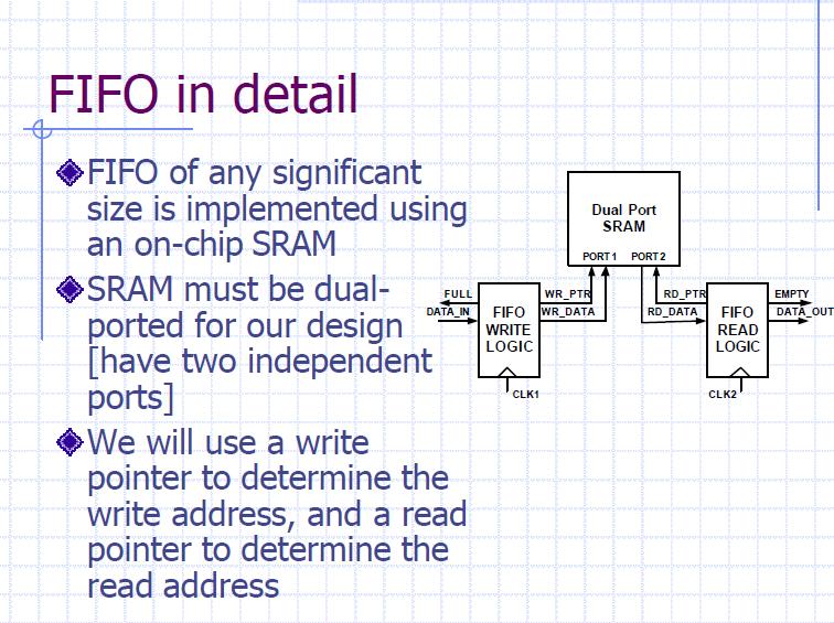
27 Sync FIFO behavior Once you write new data the read side would need 2 RCV cycles to understand their presence plus 1 RCV cycle to read them out When the FIFO becomes full and a read takes place the send side would require 2 SND cycles to understand that there is empty space in the FIFO plus 1 SND cycle to put a new word in the FIFO Total of 3 x rcv_cycles + 3 x snd_cycles More sync stages would increase the latency If rcv_cycle can be equal to snd_cycle (frequencies can be dynamically changing) 6 FIFO slots are needed at least
EE178 Spring 2018 Lecture Module 5. Eric Crabill
 EE178 Spring 2018 Lecture Module 5 Eric Crabill Goals Considerations for synchronizing signals Clocks Resets Considerations for asynchronous inputs Methods for crossing clock domains Clocks The academic
EE178 Lecture Module 4. Eric Crabill SJSU / Xilinx Fall 2005
 EE178 Lecture Module 4 Eric Crabill SJSU / Xilinx Fall 2005 Lecture #9 Agenda Considerations for synchronizing signals. Clocks. Resets. Considerations for asynchronous inputs. Methods for crossing clock
EE273 Lecture 14 Synchronizer Design November 11, Today s Assignment
 273 Lecture 14 Synchronizer esign November 11, 1998 William J. ally Computer Systems Laboratory Stanford University billd@csl.stanford.edu 1 Today s Assignment Term Project design a signaling system entire
EE273 Lecture 15 Synchronizer Design
 EE273 Lecture 15 Synchronizer Design March 5, 2003 Sarah L. Harris Computer Systems Laboratory Stanford University slharris@cva.stanford.edu 1 Logistics Final Exam Wednesday 3/19, 9:30AM to 11:30AM Upcoming
Figure 1 shows a simple implementation of a clock switch, using an AND-OR type multiplexer logic.
 1. CLOCK MUXING: With more and more multi-frequency clocks being used in today's chips, especially in the communications field, it is often necessary to switch the source of a clock line while the chip
Lecture 13: Clock and Synchronization. TIE Logic Synthesis Arto Perttula Tampere University of Technology Spring 2017
 Lecture 13: Clock and Synchronization TIE-50206 Logic Synthesis Arto Perttula Tampere University of Technology Spring 2017 Acknowledgements Most slides were prepared by Dr. Ari Kulmala The content of the
Clock Domain Crossing. Presented by Abramov B. 1
 Clock Domain Crossing Presented by Abramov B. 1 Register Transfer Logic Logic R E G I S T E R Transfer Logic R E G I S T E R Presented by Abramov B. 2 RTL (cont) An RTL circuit is a digital circuit composed
EECS150 - Digital Design Lecture 15 Finite State Machines. Announcements
 EECS150 - Digital Design Lecture 15 Finite State Machines October 18, 2011 Elad Alon Electrical Engineering and Computer Sciences University of California, Berkeley http://www-inst.eecs.berkeley.edu/~cs150
EITF35: Introduction to Structured VLSI Design
 EITF35: Introduction to Structured VLSI Design Part 4.2.1: Learn More Liang Liu liang.liu@eit.lth.se 1 Outline Crossing clock domain Reset, synchronous or asynchronous? 2 Why two DFFs? 3 Crossing clock
EECS 373 Design of Microprocessor-Based Systems
 EECS 373 Design of Microprocessor-Based Systems Matt Smith University of Michigan Serial buses, digital design Material taken from Brehob, Dutta, Le, Ramadas, Tikhonov & Mahal 1 Agenda Serial Buses Introduction
https://daffy1108.wordpress.com/2014/06/08/synchronizers-for-asynchronous-signals/
 https://daffy1108.wordpress.com/2014/06/08/synchronizers-for-asynchronous-signals/ Synchronizers for Asynchronous Signals Asynchronous signals causes the big issue with clock domains, namely metastability.
EECS150 - Digital Design Lecture 10 - Interfacing. Recap and Topics
 EECS150 - Digital Design Lecture 10 - Interfacing Oct. 1, 2013 Prof. Ronald Fearing Electrical Engineering and Computer Sciences University of California, Berkeley (slides courtesy of Prof. John Wawrzynek)
EECS150 - Digital Design Lecture 19 - Finite State Machines Revisited
 EECS150 - Digital Design Lecture 19 - Finite State Machines Revisited April 2, 2013 John Wawrzynek Spring 2013 EECS150 - Lec19-fsm Page 1 Finite State Machines (FSMs) FSM circuits are a type of sequential
Universal Asynchronous Receiver- Transmitter (UART)
") Universal Asynchronous Receiver- Transmitter (UART) (UART) Block Diagram Four-Bit Bidirectional Shift Register Shift Register Counters Shift registers can form useful counters by recirculating a pattern
Universal Asynchronous Receiver- Transmitter (UART) (UART) Block Diagram Four-Bit Bidirectional Shift Register Shift Register Counters Shift registers can form useful counters by recirculating a pattern
Digital System Design
 Digital System Design by Dr. Lesley Shannon Email: lshannon@ensc.sfu.ca Course Website: http://www.ensc.sfu.ca/~lshannon/courses/ensc350 Simon Fraser University Slide Set: 8 Date: February 9, 2009 Timing
DEDICATED TO EMBEDDED SOLUTIONS
 DEDICATED TO EMBEDDED SOLUTIONS DESIGN SAFE FPGA INTERNAL CLOCK DOMAIN CROSSINGS ESPEN TALLAKSEN DATA RESPONS SCOPE Clock domain crossings (CDC) is probably the worst source for serious FPGA-bugs that
Asynchronous (Ripple) Counters
 Counters") Circuits for counting events are frequently used in computers and other digital systems. Since a counter circuit must remember its past states, it has to possess memory. The chapter about flip-flops introduced
Circuits for counting events are frequently used in computers and other digital systems. Since a counter circuit must remember its past states, it has to possess memory. The chapter about flip-flops introduced
L4: Sequential Building Blocks (Flip-flops, Latches and Registers)
") L4: Sequential Building Blocks (Flip-flops, Latches and Registers) Acknowledgements: Lecture material adapted from R. Katz, G. Borriello, Contemporary Logic esign (second edition), Prentice-Hall/Pearson
L4: Sequential Building Blocks (Flip-flops, Latches and Registers) Acknowledgements: Lecture material adapted from R. Katz, G. Borriello, Contemporary Logic esign (second edition), Prentice-Hall/Pearson
EE241 - Spring 2005 Advanced Digital Integrated Circuits
 EE241 - Spring 2005 Advanced Digital Integrated Circuits Lecture 21: Asynchronous Design Synchronization Clock Distribution Self-Timed Pipelined Datapath Req Ack HS Req Ack HS Req Ack HS Req Ack Start
Synchronous Sequential Design
 Synchronous Sequential Design SMD098 Computation Structures Lecture 4 1 Synchronous sequential systems Almost all digital systems have some concept of state the outputs of a system depends on the past
CMOS Implementation of Reliable Synchronizer for Multi clock domain System-on-chip
 RESEARCH ARTICLE OPEN ACCESS CMOS Implementation of Reliable Synchronizer for Multi clock domain System-on-chip Vivek khetade 1, Dr. S.S. Limaye 2 Sarang Purnaye 3 1 Department of Electronic design Technology,
More on Flip-Flops Digital Design and Computer Architecture: ARM Edition 2015 Chapter 3 <98> 98
 More on Flip-Flops Digital Design and Computer Architecture: ARM Edition 2015 Chapter 3 98 Review: Bit Storage SR latch S (set) Q R (reset) Level-sensitive SR latch S S1 C R R1 Q D C S R D latch Q
Glitches/hazards and how to avoid them. What to do when the state machine doesn t fit!
 State Machine Signaling Timing Behavior Glitches/hazards and how to avoid them SM Partitioning What to do when the state machine doesn t fit! State Machine Signaling Introducing Idle States (synchronous
EE241 - Spring 2007 Advanced Digital Integrated Circuits. Announcements
 EE241 - Spring 2007 Advanced igital Integrated Circuits Lecture 24: Advanced Flip-Flops Synchronization Announcements Homework 5 due on 4/26 Final exam on May 8 in class Project presentations on May 3,
Asynchronous inputs. 9 - Metastability and Clock Recovery. A simple synchronizer. Only one synchronizer per input
 9 - Metastability and Clock Recovery Asynchronous inputs We will consider a number of issues related to asynchronous inputs, multiple clock domains, clock synchronisation and clock distribution. Useful
Clock and Asynchronous Signals
 Clock and Asynchronous Signals Z. Jerry Shi Computer Science and Engineering University of Connecticut Thank John Wakerly for providing his slides and figures. Functional timing Delays in state machines
Counter dan Register
 Counter dan Register Introduction Circuits for counting events are frequently used in computers and other digital systems. Since a counter circuit must remember its past states, it has to possess memory.
Outline. EECS150 - Digital Design Lecture 27 - Asynchronous Sequential Circuits. Cross-coupled NOR gates. Asynchronous State Transition Diagram
 EECS150 - Digital Design Lecture 27 - Asynchronous Sequential Circuits Nov 26, 2002 John Wawrzynek Outline SR Latches and other storage elements Synchronizers Figures from Digital Design, John F. Wakerly
EE273 Lecture 11 Pipelined Timing Closed-Loop Timing November 2, Today s Assignment
 EE273 Lecture 11 Pipelined Timing Closed-Loop Timing November 2, 1998 William J. ally Computer Systems Laboratory Stanford University billd@csl.stanford.edu Copyright (C) by William J. ally, All Rights
Synchronization in Asynchronously Communicating Digital Systems
 Synchronization in Asynchronously Communicating Digital Systems Priyadharshini Shanmugasundaram Abstract Two digital systems working in different clock domains require a protocol to communicate with each
EECS 373 Design of Microprocessor-Based Systems
 EECS 373 Design of Microprocessor-Based Systems Mark Brehob University of Michigan Lecture 13: Wrapping up and moving forward. Review error with ADCs/DACs Finish design rules Quick discussion of MMIO in
FIFO Memories: Solution to Reduce FIFO Metastability
 FIFO Memories: Solution to Reduce FIFO Metastability First-In, First-Out Technology Tom Jackson Advanced System Logic Semiconductor Group SCAA011A March 1996 1 IMPORTANT NOTICE Texas Instruments (TI) reserves
Metastability Analysis of Synchronizer
 Forn International Journal of Scientific Research in Computer Science and Engineering Research Paper Vol-1, Issue-3 ISSN: 2320 7639 Metastability Analysis of Synchronizer Ankush S. Patharkar *1 and V.
EECS 373 Design of Microprocessor-Based Systems
 EECS 373 Design of Microprocessor-Based Systems A day of Misc. Topics Mark Brehob University of Michigan Lecture 12: Finish up Analog and Digital converters Finish design rules Quick discussion of MMIO
Lec 24 Sequential Logic Revisited Sequential Circuit Design and Timing
 Traversing igital esign EECS - Components and esign Techniques for igital Systems EECS wks 6 - Lec 24 Sequential Logic Revisited Sequential Circuit esign and Timing avid Culler Electrical Engineering and
Chapter 3 Unit Combinational
 EE 200: Digital Logic Circuit Design Dr Radwan E Abdel-Aal, COE Logic and Computer Design Fundamentals Chapter 3 Unit Combinational 5 Registers Logic and Design Counters Part Implementation Technology
ESE 570 STATIC SEQUENTIAL CMOS LOGIC CELLS. Kenneth R. Laker, University of Pennsylvania, updated 25Mar15
 ESE 570 STATIC SEQUENTIAL CMOS LOGIC CELLS 1 Classes of Logic Circuits two stable op. pts. Latch level triggered. Flip-Flop edge triggered. one stable op. pt. One-shot single pulse output no stable op.
problem maximum score 1 28pts 2 10pts 3 10pts 4 15pts 5 14pts 6 12pts 7 11pts total 100pts
 University of California at Berkeley College of Engineering Department of Electrical Engineering and Computer Sciences EECS150 J. Wawrzynek Spring 2002 4/5/02 Midterm Exam II Name: Solutions ID number:
TKT-1212 Digitaalijärjestelmien toteutus. Lecture 13 - Clock and Synchronization Erno Salminen, Spring 2013
 TKT-1212 Digitaalijärjestelmien toteutus Lecture 13 - Clock and Synchronization Erno Salminen, Spring 2013 Acknowledgements Most slides were prepared by Dr. Ari Kulmala The content of the slides are partially
Synchronizers and Arbiters
 Synchronizers and Arbiters David Kinniment University of Newcastle Tutorial 7 April 2008 1 Outline What s the problem? Why does it matter? Synchronizer and arbiter circuits Noise, and its effects Latency,
Digital Logic & Computer Design CS Professor Dan Moldovan Spring Chapter 3 :: Sequential Logic Design
 igital Logic & Computer esign CS 4341 Professor an Moldovan Spring 21 Copyright 27 Elsevier 3- Chapter 3 :: Sequential Logic esign igital esign and Computer Architecture avid Money Harris and Sarah
Sequential Circuits. Sequential Logic. Circuits with Feedback. Simplest Circuits with Feedback. Memory with Cross-coupled Gates.
 equential Logic equential Circuits equential Circuits imple circuits with feedback Latches Edge-triggered flip-flops Timing Methodologies Cascading flip-flops for proper operation Clock skew Basic egisters
Robust Synchronization using the Wagging Technique
 School of Electrical, Electronic & Computer Engineering Robust Synchronization using the Wagging Technique Mohammed Alshaikh, David Kinniment, and Alex Yakovlev Technical Report Series NCL-EECE-MSD-TR-2010-165
Synchronous Sequential Logic
 Synchronous Sequential Logic -A Sequential Circuit consists of a combinational circuit to which storage elements are connected to form a feedback path. The storage elements are devices capable of storing
Chapter 6. Flip-Flops and Simple Flip-Flop Applications
 Chapter 6 Flip-Flops and Simple Flip-Flop Applications Basic bistable element It is a circuit having two stable conditions (states). It can be used to store binary symbols. J. C. Huang, 2004 Digital Logic
Unit 9 Latches and Flip-Flops. Dept. of Electrical and Computer Eng., NCTU 1
 Unit 9 Latches and Flip-Flops Dept. of Electrical and Computer Eng., NCTU 1 9.1 Introduction Dept. of Electrical and Computer Eng., NCTU 2 What is the characteristic of sequential circuits in contrast
Logic Design. Flip Flops, Registers and Counters
 Logic Design Flip Flops, Registers and Counters Introduction Combinational circuits: value of each output depends only on the values of inputs Sequential Circuits: values of outputs depend on inputs and
Computer Science 324 Computer Architecture Mount Holyoke College Fall Topic Notes: Sequential Circuits
 Computer Science 324 Computer Architecture Mount Holyoke College Fall 2007 opic Notes: Sequential Circuits Let s think about how life can be bad for a circuit. Edge Detection Consider this one: What is
! Two inverters form a static memory cell " Will hold value as long as it has power applied
 equential Logic! equential Circuits " imple circuits with feedback " Latches " Edge-triggered flip-flops! Timing Methodologies " Cascading flip-flops for proper operation " Clock skew! Basic egisters "
Sequential Logic. Sequential Circuits. ! Timing Methodologies " Cascading flip-flops for proper operation " Clock skew
 equential Logic! equential Circuits " imple circuits with feedback " Latches " Edge-triggered flip-flops! Timing Methodologies " Cascading flip-flops for proper operation " Clock skew! Basic egisters "
CSE115: Digital Design Lecture 23: Latches & Flip-Flops
 Faculty of Engineering CSE115: Digital Design Lecture 23: Latches & Flip-Flops Sections 7.1-7.2 Suggested Reading A Generic Digital Processor Building Blocks for Digital Architectures INPUT - OUTPUT Interconnect:
ECE321 Electronics I
 ECE321 Electronics I Lecture 25: Sequential Logic: Flip-flop Payman Zarkesh-Ha Office: ECE Bldg. 230B Office hours: Tuesday 2:00-3:00PM or by appointment E-mail: pzarkesh.unm.edu Slide: 1 Review of Last
Product Level MTBF Calculation
 2014 Fifth International Conference on Intelligent Systems, Modelling and Simulation Product Level MTBF Calculation Ang Boon Chong easic Corp bang@easic.com Abstract Synchronizers are used in sampling
EEC 118 Lecture #9: Sequential Logic. Rajeevan Amirtharajah University of California, Davis Jeff Parkhurst Intel Corporation
 EEC 118 Lecture #9: Sequential Logic Rajeevan Amirtharajah University of California, Davis Jeff Parkhurst Intel Corporation Outline Review: Static CMOS Logic Finish Static CMOS transient analysis Sequential
The outputs are formed by a combinational logic function of the inputs to the circuit or the values stored in the flip-flops (or both).
.") 1 The outputs are formed by a combinational logic function of the inputs to the circuit or the values stored in the flip-flops (or both). The value that is stored in a flip-flop when the clock pulse occurs
1 The outputs are formed by a combinational logic function of the inputs to the circuit or the values stored in the flip-flops (or both). The value that is stored in a flip-flop when the clock pulse occurs
Automated Verification and Clock Frequency Characteristics in CDC Solution
 Int. J. Com. Dig. Sys. 2, No. 1, 1-8 (2013) 1 International Journal of Computing and Digital Systems @ 2013 UOB CSP, University of Bahrain Automated Verification and Clock Frequency Characteristics in
INTRODUCTION TO SEQUENTIAL CIRCUITS
 NOTE: Explanation Refer Class Notes Digital Circuits(15EECC203) INTRODUCTION TO SEQUENTIAL CIRCUITS by Nagaraj Vannal, Asst.Professor, School of Electronics Engineering, K.L.E. Technological University,
Outcomes. Spiral 1 / Unit 6. Flip-Flops FLIP FLOPS AND REGISTERS. Flip-flops and Registers. Outputs only change once per clock period
 1-6.1 1-6.2 Outcomes Spiral 1 / Unit 6 Flip-flops and Registers I know the difference between combinational and sequential logic and can name examples of each. I understand latency, throughput, and at
Computer Science 324 Computer Architecture Mount Holyoke College Fall Topic Notes: Sequential Circuits
 Computer Science 324 Computer Architecture Mount Holyoke College Fall 2009 opic Notes: Sequential Circuits Let s think about how life can be bad for a circuit. Edge Detection Consider this one: What is
ECEN454 Digital Integrated Circuit Design. Sequential Circuits. Sequencing. Output depends on current inputs
 ECEN454 igital Integrated Circuit esign Sequential Circuits ECEN 454 Combinational logic Sequencing Output depends on current inputs Sequential logic Output depends on current and previous inputs Requires
Sequential Logic. E&CE 223 Digital Circuits and Systems (A. Kennings) Page 1
 Page 1") Sequential Logic E&CE 223 igital Circuits and Systems (A. Kennings) Page 1 Sequential Circuits Have considered only combinational circuits in which circuit outputs are determined entirely by current circuit
Sequential Logic E&CE 223 igital Circuits and Systems (A. Kennings) Page 1 Sequential Circuits Have considered only combinational circuits in which circuit outputs are determined entirely by current circuit
EEE2135 Digital Logic Design Chapter 6. Latches/Flip-Flops and Registers/Counters 서강대학교 전자공학과
 EEE235 Digital Logic Design Chapter 6. Latches/Flip-Flops and Registers/Counters 서강대학교 전자공학과 . Delay and Latches ) Signal Storage a. as voltage level static memory b. as charges dynamic memory 2) Delays
EE141-Fall 2010 Digital Integrated Circuits. Announcements. Homework #8 due next Tuesday. Project Phase 3 plan due this Sat.
 EE141-Fall 2010 Digital Integrated Circuits Lecture 24 Timing 1 1 Announcements Homework #8 due next Tuesday Project Phase 3 plan due this Sat. Hanh-Phuc s extra office hours shifted next week Tues. 3-4pm
Digital Design, Kyung Hee Univ. Chapter 5. Synchronous Sequential Logic
 Chapter 5. Synchronous Sequential Logic 1 5.1 Introduction Electronic products: ability to send, receive, store, retrieve, and process information in binary format Dependence on past values of inputs Sequential
EECS150 - Digital Design Lecture 3 - Timing
 EECS150 - Digital Design Lecture 3 - Timing January 29, 2002 John Wawrzynek Spring 2002 EECS150 - Lec03-Timing Page 1 Outline General Model of Synchronous Systems Performance Limits Announcements Delay
Metastability and Synchronizers A Tutorial
 Metastability and Synchronizers A Tutorial Ran Ginosar VLSI Systems Research Center Electrical Engineering and Computer Science Departments Technion Israel Institute of Technology, Haifa 32000, Israel
PRE J. Figure 25.1a J-K flip-flop with Asynchronous Preset and Clear inputs
 Asynchronous Preset and Clear Inputs The S-R, J-K and D inputs are known as synchronous inputs because the outputs change when appropriate input values are applied at the inputs and a clock signal is applied
Asynchronous Counter
 Asynchronous Counter Contents: Asynchronous/Ripple Counter Propagation Delay in Ripple Counter MOD Number Synchronous/Parallel Counter 10101010101010101010101010101010101010101010101010101010101010101010101010101010
Lecture 8: Sequential Logic
 Lecture 8: Sequential Logic Last lecture discussed how we can use digital electronics to do combinatorial logic we designed circuits that gave an immediate output when presented with a given set of inputs
Unit 11. Latches and Flip-Flops
 Unit 11 Latches and Flip-Flops 1 Combinational Circuits A combinational circuit consists of logic gates whose outputs, at any time, are determined by combining the values of the inputs. For n input variables,
cascading flip-flops for proper operation clock skew Hardware description languages and sequential logic
 equential logic equential circuits simple circuits with feedback latches edge-triggered flip-flops Timing methodologies cascading flip-flops for proper operation clock skew Basic registers shift registers
Sequential logic. Circuits with feedback. How to control feedback? Sequential circuits. Timing methodologies. Basic registers
 equential logic equential circuits simple circuits with feedback latches edge-triggered flip-flops Timing methodologies cascading flip-flops for proper operation clock skew Basic registers shift registers
Other Flip-Flops. Lecture 27 1
 Other Flip-Flops Other types of flip-flops can be constructed by using the D flip-flop and external logic. Two flip-flops less widely used in the design of digital systems are the JK and T flip-flops.
Logic and Computer Design Fundamentals. Chapter 7. Registers and Counters
 Logic and Computer Design Fundamentals Chapter 7 Registers and Counters Registers Register a collection of binary storage elements In theory, a register is sequential logic which can be defined by a state
Counters
 Counters A counter is the most versatile and useful subsystems in the digital system. A counter driven by a clock can be used to count the number of clock cycles. Since clock pulses occur at known intervals,
Traversing Digital Design. EECS Components and Design Techniques for Digital Systems. Lec 22 Sequential Logic - Advanced
 Traversing igital esign EEC 5 - Components and esign Techniques for igital ystems EEC5 wks 6-5 Lec 22 equential Logic - Advanced avid Culler Electrical Engineering and Computer ciences University of California,
More Digital Circuits
 More Digital Circuits 1 Signals and Waveforms: Showing Time & Grouping 2 Signals and Waveforms: Circuit Delay 2 3 4 5 3 10 0 1 5 13 4 6 3 Sample Debugging Waveform 4 Type of Circuits Synchronous Digital
The NOR latch is similar to the NAND latch
 5-2 NOR Gate Latch The NOR latch is similar to the NAND latch except that the Q and Q outputs are reversed. The set and clear inputs are active high, that is, the output will change when the input is pulsed
6.S084 Tutorial Problems L05 Sequential Circuits
 Preamble: Sequential Logic Timing 6.S084 Tutorial Problems L05 Sequential Circuits In Lecture 5 we saw that for D flip-flops to work correctly, the flip-flop s input should be stable around the rising
Chapter 1: Switching Algebra Chapter 2: Logical Levels, Timing & Delays. Introduction to latches Chapter 9: Binary Arithmetic
 12.12.216 Chapter 5 Flip Flops Dr.-ng. Stefan Werner /14 Table of content Chapter 1: Switching Algebra Chapter 2: Logical Levels, Timing & Delays Chapter 3: Karnaugh-Veitch-Maps Chapter 4: Combinational
EE141-Fall 2010 Digital Integrated Circuits. Announcements. Synchronous Timing. Latch Parameters. Class Material. Homework #8 due next Tuesday
 EE-Fall 00 Digital tegrated Circuits Timing Lecture Timing Announcements Homework #8 due next Tuesday Synchronous Timing Project Phase plan due this Sat. Hanh-Phuc s extra office hours shifted next week
Chapter 6. sequential logic design. This is the beginning of the second part of this course, sequential logic.
 Chapter 6. sequential logic design This is the beginning of the second part of this course, sequential logic. 1 equential logic equential circuits simple circuits with feedback latches edge-triggered flip-flops
EMT 125 Digital Electronic Principles I CHAPTER 6 : FLIP-FLOP
 EMT 125 Digital Electronic Principles I CHAPTER 6 : FLIP-FLOP 1 Chapter Overview Latches Gated Latches Edge-triggered flip-flops Master-slave flip-flops Flip-flop operating characteristics Flip-flop applications
CHAPTER 6 COUNTERS & REGISTERS
 CHAPTER 6 COUNTERS & REGISTERS 6.1 Asynchronous Counter 6.2 Synchronous Counter 6.3 State Machine 6.4 Basic Shift Register 6.5 Serial In/Serial Out Shift Register 6.6 Serial In/Parallel Out Shift Register
Registers and Counters
 Registers and Counters Clocked sequential circuit = F/Fs and combinational gates Register Group of flip-flops (share a common clock and capable of storing one bit of information) Consist of a group of
EECS150 - Digital Design Lecture 3 - Timing
 EECS150 - Digital Design Lecture 3 - Timing September 3, 2002 John Wawrzynek Fall 2002 EECS150 - Lec03-Timing Page 1 Outline Finish up from lecture 2 General Model of Synchronous Systems Performance Limits
6. Sequential Logic Flip-Flops
 ection 6. equential Logic Flip-Flops Page of 5 6. equential Logic Flip-Flops ombinatorial components: their output values are computed entirely from their present input values. equential components: their
Advanced Digital Logic Design EECS 303
 Advanced Digital Logic Design EECS 303 http://ziyang.eecs.northwestern.edu/eecs303/ Teacher: Robert Dick Office: L477 Tech Email: dickrp@northwestern.edu Phone: 847 467 2298 Outline Introduction Reset/set
Digital Logic Design ENEE x. Lecture 19
 Digital Logic Design ENEE 244-010x Lecture 19 Announcements Homework 8 due on Monday, 11/23. Agenda Last time: Timing Considerations (6.3) Master-Slave Flip-Flops (6.4) This time: Edge-Triggered Flip-Flops
DEPARTMENT OF ELECTRICAL &ELECTRONICS ENGINEERING DIGITAL DESIGN
 DEPARTMENT OF ELECTRICAL &ELECTRONICS ENGINEERING DIGITAL DESIGN Assoc. Prof. Dr. Burak Kelleci Spring 2018 OUTLINE Synchronous Logic Circuits Latch Flip-Flop Timing Counters Shift Register Synchronous
Introduction. NAND Gate Latch. Digital Logic Design 1 FLIP-FLOP. Digital Logic Design 1
 2007 Introduction BK TP.HCM FLIP-FLOP So far we have seen Combinational Logic The output(s) depends only on the current values of the input variables Here we will look at Sequential Logic circuits The
CS 110 Computer Architecture. Finite State Machines, Functional Units. Instructor: Sören Schwertfeger.
 CS 110 Computer Architecture Finite State Machines, Functional Units Instructor: Sören Schwertfeger http://shtech.org/courses/ca/ School of Information Science and Technology SIST ShanghaiTech University
Momentary Changes in Outputs. State Machine Signaling. Oscillatory Behavior. Hazards/Glitches. Types of Hazards. Static Hazards
 State Machine Signaling Momentary hanges in Outputs Timing ehavior Glitches/hazards and how to avoid them SM Partitioning What to do when the state machine doesn t fit! State Machine Signaling State Machine
EL302 DIGITAL INTEGRATED CIRCUITS LAB #3 CMOS EDGE TRIGGERED D FLIP-FLOP. Due İLKER KALYONCU, 10043
 EL302 DIGITAL INTEGRATED CIRCUITS LAB #3 CMOS EDGE TRIGGERED D FLIP-FLOP Due 16.05. İLKER KALYONCU, 10043 1. INTRODUCTION: In this project we are going to design a CMOS positive edge triggered master-slave
Sequential Circuit Design: Principle
 Sequential Circuit Design: Principle modified by L.Aamodt 1 Outline 1. 2. 3. 4. 5. 6. 7. 8. Overview on sequential circuits Synchronous circuits Danger of synthesizing asynchronous circuit Inference of
CSE140: Components and Design Techniques for Digital Systems. More D-Flip-Flops. Tajana Simunic Rosing. Sources: TSR, Katz, Boriello & Vahid
 CSE140: Components and esign Techniques for igital Systems More -Flip-Flops Tajana Simunic Rosing Where we are now. What we covered last time: SRAM cell, SR latch, latch, -FF What we ll do next: -FF review,
Sequencing. Lan-Da Van ( 范倫達 ), Ph. D. Department of Computer Science National Chiao Tung University Taiwan, R.O.C. Fall,
, Ph. D. Department of Computer Science National Chiao Tung University Taiwan, R.O.C. Fall,") Sequencing ( 范倫達 ), Ph. D. Department of Computer Science National Chiao Tung University Taiwan, R.O.C. Fall, 2013 ldvan@cs.nctu.edu.tw http://www.cs.nctu.edu.tw/~ldvan/ Outlines Introduction Sequencing
Sequencing ( 范倫達 ), Ph. D. Department of Computer Science National Chiao Tung University Taiwan, R.O.C. Fall, 2013 ldvan@cs.nctu.edu.tw http://www.cs.nctu.edu.tw/~ldvan/ Outlines Introduction Sequencing
Measurements of metastability in MUTEX on an FPGA
 LETTER IEICE Electronics Express, Vol.15, No.1, 1 11 Measurements of metastability in MUTEX on an FPGA Nguyen Van Toan, Dam Minh Tung, and Jeong-Gun Lee a) E-SoC Lab/Smart Computing Lab, Dept. of Computer
Combinational vs Sequential
 Combinational vs Sequential inputs X Combinational Circuits outputs Z A combinational circuit: At any time, outputs depends only on inputs Changing inputs changes outputs No regard for previous inputs
CPE/EE 427, CPE 527 VLSI Design I Sequential Circuits. Sequencing
 CPE/EE 427, CPE 527 VLSI esign I Sequential Circuits epartment of Electrical and Computer Engineering University of Alabama in Huntsville Aleksandar Milenkovic ( www.ece.uah.edu/~milenka ) Combinational