Lecture 13: Clock and Synchronization. TIE Logic Synthesis Arto Perttula Tampere University of Technology Spring 2017
|
|
|
- Philomena Blair
- 5 years ago
- Views:
Transcription


1 Lecture 13: Clock and Synchronization TIE Logic Synthesis Arto Perttula Tampere University of Technology Spring 2017
2 Acknowledgements Most slides were prepared by Dr. Ari Kulmala The content of the slides are partially courtesy of Ran Ginosar Pong P. Chu C.E. Cummings, D. Mills, Synchronous Resets? Asynchronous Resets? I am so confused! How will I ever know which to use? Recommended reading: Understanding Metastability in FPGAs, white paper, Altera Corporation July 2009 D. Chen, D. Singh, J. Chromczak, D. Lewis, R. Fung, D. Neto and V. Betz, A Comprehensive Approach to Modeling, Characterizing and Optimizing for Metastability in FPGAs, ACM International Symposium on Field Programmable Gate Arrays, 2010, pp R. Ginosar, Fourteen ways to fool your synchronizer, Ninth International Symposium on Asynchronous Circuits and Systems, May 2003, pp R. Ginosar, Metastability and Synchronizers: A Tutorial, IEEE D&T Comp, Sep/Oct 2011 C.E. Cummings, D. Mills, S. Golson, Asynchoronous & Synchronous Reset Design Techniques Part Deux, SNUG Boston 2003, Rev 1.2, 38 pages 2
3 Contents Synchronizer Enable tick Handshaking and derived clocks Reset synchronization 3
4 SYNCHRONIZER 4
5 Synchronization Circuit Synchronizes an asynchronous data input with system clock In general No physical circuit can prevent metastability We cannot avoid it, we have to live with it Design should be metastability-tolerant, since it cannot be metastability-free Synchronizer just provides enough time for the metastable condition to be resolved Later examples assuming these values for MTBF calculations ω = 66ps, = 33 ps, f d = 0.1f clk, f clk =200MHz (hence T c = 5ns) T setup = very small, say 0.1 ns 5

6 6

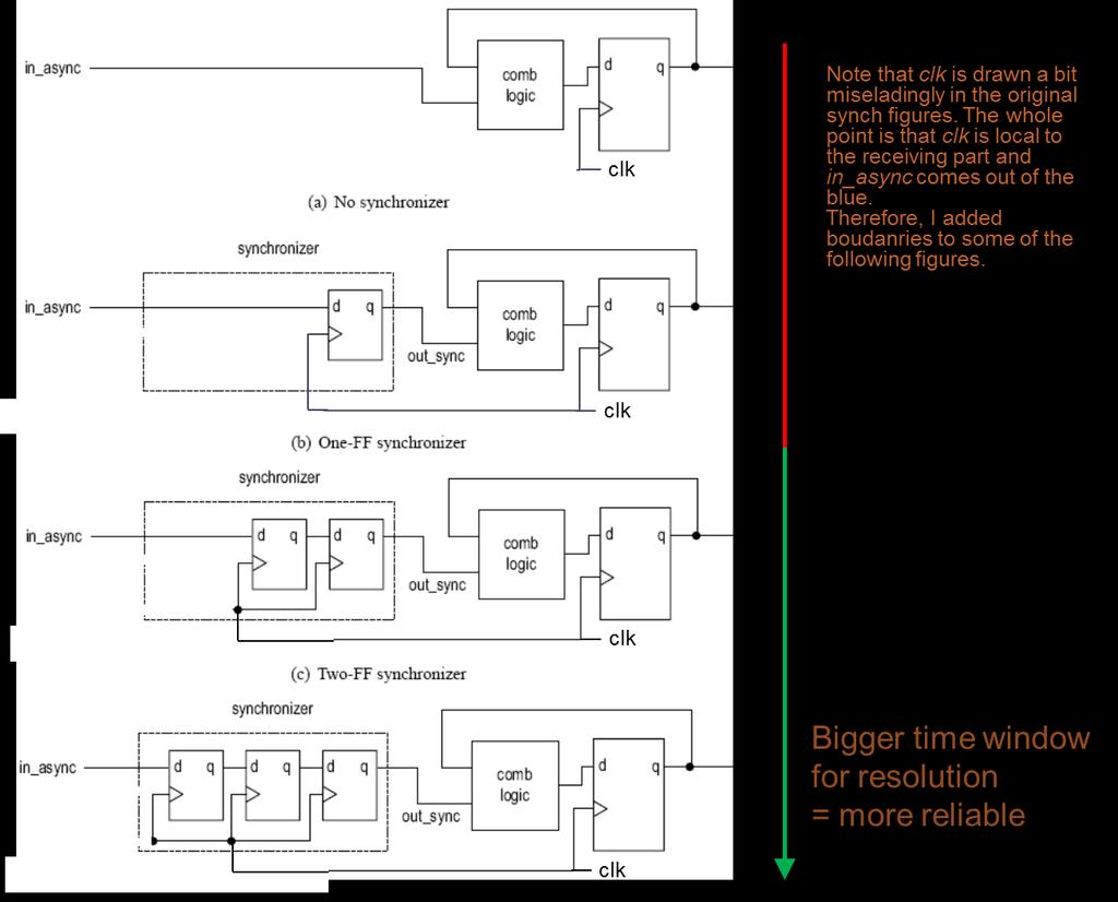
7 Wrong: No Synchronizer T r = 0 MTBF(0) = 3.8 us Donnerwetter! Dies instantly! Don t do this. Note: in book, the example MTBFs are counted with older technology, whereas in these slides with the values presented earlier clk 7
8 Wrong: One-FF Synchronizer T r = T c (T comb + T setup ) T r depends on T c, T setup and T comb T c varies with system specification (clock period) T comb varies with circuit, synthesis (gate delay), placement & routing (wire delay) E.g., T r = 5ns (T comb + 0.1ns ) = 4.9ns T comb T comb = 4 ns, T r = 0.9 ns; MTBF(0.9) = 31 days Not a reliable design Don t do this. 8
=3.7*1051 years Most commonly used synchronizer Some ASIC technologies may have metastability-hardened DFF cell (large area) Arto Perttula 8.2.2017clk")
9 The Right-Way: Two-FF Synchronizer Add an extra FF to eliminate T comb T r = T c T setup T r depends on T c only! Asynchronous input delayed by two clock cycles E.g., Tr=5ns 0.1ns= 4.9ns; MTBF(4.9)=3.7*1051 years Most commonly used synchronizer Some ASIC technologies may have metastability-hardened DFF cell (large area) Arto Perttula clk
10 Super-Safe: Multi-Stage Synchronizer Add extra stages to increase resolution time E.g., T r = (n stages -1)*(T c T setup ) Asynchronous input delayed by three clock cycles Each stage adds one clock cycle more to resolution time Increasingly unlikely that all go metastable Tr =2*(5ns 0.1ns); MTBF(9.8)=1.1* years Extremely safe but still practical 10
11 Allowed resolution time Tr can be interpret as slack time before combinatorial logic T r = T c (T comb + T setup ) T r = T c T setup T r = 2(T c T setup) ) 11
12 6 Cases of Synchronizer Timing Case a = Q1 goes 1 as wished f = Q1 goes metastable, goes randomly to 1 and resolves to 1; looks like case a b = Q1 misses 1 at first but rises at cycle 2 d = Q1 goes metastable, stays 0 and resolves to 0; looks like case b [R. Ginosar, Metastability and Synchronizers : A Tutorial, IEEE D&T Comp, Sep/Oct 2011] c = Q1 metastable but resolves to 1 within one cycle d = Q1 metastable and goes first 1 but then resolves to 0 Hence, Q2 rises all cases, but the cycle is either on 2 or 3. Note that D1 stays stable long enough 12
13 Beware of WRONG Two-FF Synchronizers! Asynchronous input contains both data and control This does NOT work ctrl data Async input 1 n+1 n FF1 FF2 CL FF3 other_clk Recall: we do not know what state the flip-flop gets after metastable event The data may get corrupted Note that some bits may be sampled correctly while some will go metastable clock Arto Perttula Ran Ginosar
14 Proper Use of Synchronizer Use a glitch-free signal for synchronization The signals between clock domains must come from a register Synchronize a signal in a single place Separate synchronization logic to a different module Avoid catastrophic parallel synchronizers Reanalyze the synchronizer after each design change... Arto Perttula
15 AN ENABLE TICK THAT CROSSES CLOCK DOMAIN 15
16 Signals That Cross Clock Domains Need synchronizer Just ensures that the receiving system does not enter a metastable state Does not guarantee the function of the received signal. The value may be wrong but at least it is truly 0 or 1 Consideration 1. One signal 2. Multiple signals ( bundled data ) 16
17 Domain-Crossing of an Enable Signal An enable tick pulse that denotes new data To be sampled on a single clock edge E.g., enable input of a counter; read/write signal of a FIFO buffer Can also be used to retrieve bundled data We need an edge detector in order to know that a new data has arrived Don t even think of using event construct in VHDL. Grrr! Depending on frequencies, the enable tick is either a) wide from slow to fast domain b) narrow from fast to slow domain 17
18 Wide Enable Signal From a slow clock domain to a fast clock domain (e.g., 1 MHz to 10 MHz) Typical user I/O has very wide pulse from the digital circuit s point of view 18
19 Narrow Enable Signal From a fast clock domain to a slow clock domain (e.g., 10 MHz to 1 MHz) The enable pulse is too narrow to be detected Very short pulse occurs somewhere between the clock edges It is never stored into synchronizing DFF We need to stretch the pulse Cannot be done by a normal sequential circuit Do not use tricks The right way to do: handshaking circuit 19
20 Transferring data between clock domains reliably HANDSHAKING 20
21 General Problems in Data Communication How to know that a new data is coming/data has been read? How to know that receiver is ready? Does the sending system have prior knowledge about the processing speed of receiving system? How to control the rate of data (or number of enable ticks) between two clock domains? (e.g., 10 MHz system to 1 MHz system) What if data was corrupted? Handshaking scheme 1. Use a feedback signal 2. Make minimal assumption about the receiving system 21

22 Wide Pulse Problem Visualized 22
23 A Solution We need handshake control signals 1. Write_request (tx rx, downstream) 2. Acknowledge (rx tx, upstream) These are transition-triggered, not level triggered! Change in signal state implies new data, not the level of the signal (0 or 1) So called Two-phase handshake protocol Does not depend on the relative clock frequencies Only the 1-bit control signal is synchronized! Never use synchronizers for data Control and data may arrive at slightly different time on opposite sides of a clock edge! The other is sampled whereas the other is not. Paha paha! Data is fed directly to the another clock domain s registers 23
24 The Right Way: Asynchronous Data load is directed by multiplexer (or flip-flop enable) Data Only 1-bit control synchronized Synchronous to clk_b 0 1 D Q Control Data has lots of time to stabilize while the control signal is being synchronized Note that the multiplexer select signal may need more complex logic D Q D Q Edge det clk_b 24

25 A Block Diagram for Handshake Transfer 25

26 Transition Triggered Example: Send Two Values 0xf and 0x2 26
27 Why Data Is Not Synchronized? How Do We Make Sure It Is Not Corrupted? When data is issued to the rx, it is not read in to any register yet Data is read to the target domain s input register after the control signal has been received reliably Synchronization delay Data could be issued before the request to be sure How long it takes for the data to propagate to receiver? Is wire delay in data larger than in request signal? If request signal is sent first and the rx block is very fast, out data y not be arrived yet when sampled However, this is not very typical Usually issuing them on the same edge suffices if the required timing constraints have been set (i.e., make sure that data is valid before request) We can be sure that when request is detected by rx, the data is stabilized If data is stable, it cannot violate the FF timings, so it is safe to read to the FFs 27
28 Why the Proposed Method Is Safe? E.g., the tx sends data, it sets signal request 0 1 If it drives the synchronizer to metastability, it resolves to 0 or 1 (provided large enough MTBF) a) If it resolves to 0 then No change detected in signal However, in next clock cycle, the FF is loaded with the right value one clock cycle delay on transfer b) If it resolves to 1 then Change detected, proceed as normally No chance for erraneous interpretation of data transmission/acknowledge 28
29 Observations Performance, clock cycles per transfer: 0-1 cc for Rx synchronizer metastability resolution 3 cc for Rx to issue ack (2 for synch, 1 for putting ack to outreg) 0-1 cc for Tx synchronizer metastability resolution 2 cc for Tx to synchronize ack 5-7 clock cycles per transfer (compare to 1 in totally synchronous) Domain crossing is slow! Other methods for data transfer 1. FIFO (syncronization needed for empty and full status signal) May perform quite well for large data chunks 2. Shared memory (synchronization needed for arbitration circuit) 3. Dual-port memory (meta-stable condition may occur in the internal arbitration circuit) These also need the synchronization! Domain crossing is still tricky and slow! 29

30 Observations (2): Don t Over-Optimize It is not beneficial to fine-tune all frequencies E.g., increasing tx clock MHz Needs synchronizers ~5% increase in Tx processing power ~5x decrease in transfer rate Tx Rx The overall performance might be better with lower frequency Same phenomenon happens with supply voltages and voltage converters/regulators One must analyze when multiple clocks pays off Depends on frequencies (e.g., 400 vs. 500 MHz) Depends on computation vs. communication ratio (e.g., ops/sent_byte) 30

31 Gray FIFO Pointers use gray code: only a single bit changes at a time Hence, the whole pointer can be synchronized although it has multiple bits. Ingenious! Arto Perttula [R. Ginosar, Metastability and Syncronizers : A Tutorial, IEEE D&T Comp, Sep/Oct 2011]
32 Gray FIFO (2) Each write (read) increments write pointer (read pointer) Pointers wraparound from n-1 to 0 Number of FIFO slots must be power of 2: 2 slots,4,8 Status is decided by comparing pointer, e.g., if read_ptr == write_ptr, then FIFO is empty Synchronization adds latency in some cases It might take two cycles before consumer notices that data has been written, if FIFO was empty before that Performance degrades, but everything works When pointer values are not close to each other, both producer and consumer can operate FIFO on their own maximum frequency Synchronized pointer is always smaller than or equal to real value Writer and reader will stop before overflow or underflow will occur 32
33 Gray FIFO (3): Multiple Writes What happens if a fast writer puts many data words into FIFO before reader notices anything? Or vice versa? wptr is incremented many times and consequently many bits will change Let s assume that FIFO is empty and 4 words are written wptr = , 011, 010, 110 The trick is that the old Q value has no impact: even if all Q bits change, that alone will not cause metastability Problem occurs if multiple D bits change near clock edge at synchronizer s first DFF Only the last increment may happennearclock edge Only 1 D-bit changes (uppermost)! a) No problem, if syncronizer succeeds b) If synchronizer fails, the output will be the older value 010 That means 3 instead of 4 Reader might have to pause for one clock cycle which causes minor loss of performance but no corruption 33
34 A not-so-clever trick Planned (not necessarily realized) functionality: en_q asserted at the rising edge of en_in en_q the synchronized en_strobe then clears stretcher Asynchronous reset shall not be a part of the implementation functionality!! en_q may last over two clock cycles and thus an edge-detector is needed Note that these kind of structures are sometimes presented. However, they are case-specific and not portable and may introduce several not-so-easy to find bugs. Avoid these structures. What if en_strobe changes near en_in s edge? 34
35 Erroneous Greedy Path in Edge Detector Why bother waiting for 3 cycles. I ll tweak it a little bit Typical mistake Incorrect implementation en_r Only a single FF in this signal s path, Tr very short en_r will go metastable and therefore en_out will also. Don t do this. 35
36 DERIVED CLOCKS 36
37 Data Transfers between Derived Clock Domains If the clocks are in the same phase, the data transmission between derived clock domains is somewhat easier System is still synchronous, the flops won t go metastable This can be guaranteed by statistical timing tools, as in globally synchronous system having only one clock Normal level-sensitive logic enable can be used The signal must be observable (no pulse stretching) However, this still poses challenges to clock tree distribution E.g., Tx clk = 10 MHz (period = 100 ns), Rx clk 40 MHz (period = 25 ns) Design a circuit that narrows the 100 ns pulse to 25 ns pulse 37
38 Derived Clock Synchronizer: Implementation Applicable when knowing the relative difference beforehand E.g., when both clocks come from the same PLL, the oscillator noise and drift affect both of them equally Use a counter to detect the last clock cycle More time for data to stabilize Counter is naturally clocked at the higher of the two frequencies E.g., 4x difference in frequencies: use 0-to-3 counter When 3 is reached, a one clock cycle 1 pulse is AND ed with the actual we-signal form the tx Denoted with we_narrow in the next slide s example 38

39 Example of Derived Clock Synchronization with Slow Pulse 39
40 Derived Clock Synchronizer: Implementation When not knowing the relative difference First, we have to know which clock is faster 1. Use a feedback loop with edge detector to know whenever the slower clock has changed its state Both ends send a feedback signal that toggles every rising clock edge (=half frequency w.r.t. their own clock) 2. At rx, set one cycle long 1 -pulse (faster clock period) at the beginning of each slower clock edge Slower device may send as often as it wishes 40

41 Example of Derived Clock Synchronization, TX Slower But Actual Difference Not Known at Design Time
42 This and That -chronous Synchronous system is coordinated with global clock Isochronous the time interval between two significant moments is constant or an integer-multiple of it Isochronous transfer can start at random time w.r.t. to rx, but bits in transfer come with fixed interval Asynchronous no global clock Mesochronous tx and rx have the same frequency, but unknown phase Same clock source, but undefined clock skew due to routing Plesiochronous tx and rx are almost synchronized Both have their own oscillator with matching frequencies and all variance is within specified limits Nevertheless, the mismatch accumulates, the phase drifts
43 Clock Uncertainties [B. Nikolić, EE241 - Spring 2004 Advanced Digital Integrated Circuits, Lecture 21,
44 RESET SYNCHRONIZATION 44


45 Problem with Reset Timing Reset must fulfill reset recovery and removal time constraints No change just before or after rising clock edge E.g., the output of a flip-flop can go metastable when the reset is deasserted close to the rising edge of the clock and the output to the flip-flop must change Most problems occur when exiting reset state not entering it


46 Problem with Reset (2) Reset signal has some delay from input pin to the flip-flops Delay varies between flip-flops Asynchronous reset signal may arrive just before clock edge to some flip-flops and just after edge to some More likely the further apart the flip-flops are May go undetected, unless logic expects that certain flip-flops tick together E.g., bits from FSM state register E.g., two counters should produce exactly the same values, e.g., to generate pseudo-random numbers 46
47 Must Synchronize the Reset Also Designer must guarantee that reset signal does not change near clock edge Ensure that internal reset signal goes inactive at beginning of clock period 1. Synchronize reset input 2. The reset has a full cycle to propagate to all flip-flops Loose constraint: Domain reset delay < Domain T C (clock period) All the registers+combinational logic must be stabilized within a clock period 47


48 Reset Synchronizer On chip reset: 1. Most FFs are set or reset (so called follower DFF, e.g., in shift register, can omit reset) 2. Clocks are started 3. Reset is carefully removed Reset state is entered immediately but exited just after clock edge in the synchronizer below Global reset should be glitch-free (e.g., analog debounce logic) 48
49 Synchronous vs. Asynchronous Be careful with terminology! 1. Asynchronous vs. synchronous reset of DFF Using the dedicated input or D-input of DFF Note that latter requires running clock. Ensure that reset is active long enough (>PLL lock time) 2. Asynchronous vs. synchronized reset signal Using chip s external input directly (with undefined timing characteristics) vs. via synchronizer logic We will always synchronize the reset signal to the clock It is not that big deal whether it is connected dedicated asynchronous rst/clr input or D Was this unclear enough? 49
50 Conclusions Two flip-flops are required to synchronize asynchronous inputs Only control is synchronized, not data Clock domain crossing requires special handshaking structures The data throughput between two asynchronous clock domains is considerably less than between synchronous ones (~6x less) Synchronous derived clocks are also possible Clock routability problems Reset must also be synchronized 50
TKT-1212 Digitaalijärjestelmien toteutus. Lecture 13 - Clock and Synchronization Erno Salminen, Spring 2013
 TKT-1212 Digitaalijärjestelmien toteutus Lecture 13 - Clock and Synchronization Erno Salminen, Spring 2013 Acknowledgements Most slides were prepared by Dr. Ari Kulmala The content of the slides are partially
Lecture 12: Clock and Synchronization. TIE Logic Synthesis Arto Perttula Tampere University of Technology Spring 2018
 Lecture 12: Clock and Synchronization TIE-50206 Logic Synthesis Arto Perttula Tampere University of Technology Spring 2018 Acknowledgements Most slides were prepared by Dr. Ari Kulmala The content of the
EE178 Spring 2018 Lecture Module 5. Eric Crabill
 EE178 Spring 2018 Lecture Module 5 Eric Crabill Goals Considerations for synchronizing signals Clocks Resets Considerations for asynchronous inputs Methods for crossing clock domains Clocks The academic
EE178 Lecture Module 4. Eric Crabill SJSU / Xilinx Fall 2005
 EE178 Lecture Module 4 Eric Crabill SJSU / Xilinx Fall 2005 Lecture #9 Agenda Considerations for synchronizing signals. Clocks. Resets. Considerations for asynchronous inputs. Methods for crossing clock
https://daffy1108.wordpress.com/2014/06/08/synchronizers-for-asynchronous-signals/
 https://daffy1108.wordpress.com/2014/06/08/synchronizers-for-asynchronous-signals/ Synchronizers for Asynchronous Signals Asynchronous signals causes the big issue with clock domains, namely metastability.
EITF35: Introduction to Structured VLSI Design
 EITF35: Introduction to Structured VLSI Design Part 4.2.1: Learn More Liang Liu liang.liu@eit.lth.se 1 Outline Crossing clock domain Reset, synchronous or asynchronous? 2 Why two DFFs? 3 Crossing clock
Clock Domain Crossing. Presented by Abramov B. 1
 Clock Domain Crossing Presented by Abramov B. 1 Register Transfer Logic Logic R E G I S T E R Transfer Logic R E G I S T E R Presented by Abramov B. 2 RTL (cont) An RTL circuit is a digital circuit composed
DEDICATED TO EMBEDDED SOLUTIONS
 DEDICATED TO EMBEDDED SOLUTIONS DESIGN SAFE FPGA INTERNAL CLOCK DOMAIN CROSSINGS ESPEN TALLAKSEN DATA RESPONS SCOPE Clock domain crossings (CDC) is probably the worst source for serious FPGA-bugs that
Metastability Analysis of Synchronizer
 Forn International Journal of Scientific Research in Computer Science and Engineering Research Paper Vol-1, Issue-3 ISSN: 2320 7639 Metastability Analysis of Synchronizer Ankush S. Patharkar *1 and V.
EECS150 - Digital Design Lecture 10 - Interfacing. Recap and Topics
 EECS150 - Digital Design Lecture 10 - Interfacing Oct. 1, 2013 Prof. Ronald Fearing Electrical Engineering and Computer Sciences University of California, Berkeley (slides courtesy of Prof. John Wawrzynek)
More on Flip-Flops Digital Design and Computer Architecture: ARM Edition 2015 Chapter 3 <98> 98
 More on Flip-Flops Digital Design and Computer Architecture: ARM Edition 2015 Chapter 3 98 Review: Bit Storage SR latch S (set) Q R (reset) Level-sensitive SR latch S S1 C R R1 Q D C S R D latch Q
2.6 Reset Design Strategy
 2.6 Reset esign Strategy Many design issues must be considered before choosing a reset strategy for an ASIC design, such as whether to use synchronous or asynchronous resets, will every flipflop receive
Asynchronous inputs. 9 - Metastability and Clock Recovery. A simple synchronizer. Only one synchronizer per input
 9 - Metastability and Clock Recovery Asynchronous inputs We will consider a number of issues related to asynchronous inputs, multiple clock domains, clock synchronisation and clock distribution. Useful
Figure 1 shows a simple implementation of a clock switch, using an AND-OR type multiplexer logic.
 1. CLOCK MUXING: With more and more multi-frequency clocks being used in today's chips, especially in the communications field, it is often necessary to switch the source of a clock line while the chip
Synchronization in Asynchronously Communicating Digital Systems
 Synchronization in Asynchronously Communicating Digital Systems Priyadharshini Shanmugasundaram Abstract Two digital systems working in different clock domains require a protocol to communicate with each
The outputs are formed by a combinational logic function of the inputs to the circuit or the values stored in the flip-flops (or both).
.") 1 The outputs are formed by a combinational logic function of the inputs to the circuit or the values stored in the flip-flops (or both). The value that is stored in a flip-flop when the clock pulse occurs
1 The outputs are formed by a combinational logic function of the inputs to the circuit or the values stored in the flip-flops (or both). The value that is stored in a flip-flop when the clock pulse occurs
IT T35 Digital system desigm y - ii /s - iii
 UNIT - III Sequential Logic I Sequential circuits: latches flip flops analysis of clocked sequential circuits state reduction and assignments Registers and Counters: Registers shift registers ripple counters
Asynchronous IC Interconnect Network Design and Implementation Using a Standard ASIC Flow
 Asynchronous IC Interconnect Network Design and Implementation Using a Standard ASIC Flow Bradley R. Quinton*, Mark R. Greenstreet, Steven J.E. Wilton*, *Dept. of Electrical and Computer Engineering, Dept.
Software Engineering 2DA4. Slides 9: Asynchronous Sequential Circuits
 Software Engineering 2DA4 Slides 9: Asynchronous Sequential Circuits Dr. Ryan Leduc Department of Computing and Software McMaster University Material based on S. Brown and Z. Vranesic, Fundamentals of
VLSI Clock Domain Crossing
 VLSI Clock Domain Crossing Giorgos Dimitrakopoulos Electrical and Computer Engineering Democritus University of Thrace dimitrak@ee.duth.gr Clock relationships Asynchronous Clock domains completely unrelated
11. Sequential Elements
 11. Sequential Elements Jacob Abraham Department of Electrical and Computer Engineering The University of Texas at Austin VLSI Design Fall 2017 October 11, 2017 ECE Department, University of Texas at Austin
6.S084 Tutorial Problems L05 Sequential Circuits
 Preamble: Sequential Logic Timing 6.S084 Tutorial Problems L05 Sequential Circuits In Lecture 5 we saw that for D flip-flops to work correctly, the flip-flop s input should be stable around the rising
DEPARTMENT OF ELECTRICAL &ELECTRONICS ENGINEERING DIGITAL DESIGN
 DEPARTMENT OF ELECTRICAL &ELECTRONICS ENGINEERING DIGITAL DESIGN Assoc. Prof. Dr. Burak Kelleci Spring 2018 OUTLINE Synchronous Logic Circuits Latch Flip-Flop Timing Counters Shift Register Synchronous
Sequential Circuit Design: Principle
 Sequential Circuit Design: Principle modified by L.Aamodt 1 Outline 1. 2. 3. 4. 5. 6. 7. 8. Overview on sequential circuits Synchronous circuits Danger of synthesizing asynchronous circuit Inference of
Timing Error Detection: An Adaptive Scheme To Combat Variability EE241 Final Report Nathan Narevsky and Richard Ott {nnarevsky,
 Timing Error Detection: An Adaptive Scheme To Combat Variability EE241 Final Report Nathan Narevsky and Richard Ott {nnarevsky, tomott}@berkeley.edu Abstract With the reduction of feature sizes, more sources
ELCT201: DIGITAL LOGIC DESIGN
 ELCT201: DIGITAL LOGIC DESIGN Dr. Eng. Haitham Omran, haitham.omran@guc.edu.eg Dr. Eng. Wassim Alexan, wassim.joseph@guc.edu.eg Lecture 6 Following the slides of Dr. Ahmed H. Madian ذو الحجة 1438 ه Winter
Synchronous Sequential Design
 Synchronous Sequential Design SMD098 Computation Structures Lecture 4 1 Synchronous sequential systems Almost all digital systems have some concept of state the outputs of a system depends on the past
EE241 - Spring 2005 Advanced Digital Integrated Circuits
 EE241 - Spring 2005 Advanced Digital Integrated Circuits Lecture 21: Asynchronous Design Synchronization Clock Distribution Self-Timed Pipelined Datapath Req Ack HS Req Ack HS Req Ack HS Req Ack Start
Sequential logic. Circuits with feedback. How to control feedback? Sequential circuits. Timing methodologies. Basic registers
 equential logic equential circuits simple circuits with feedback latches edge-triggered flip-flops Timing methodologies cascading flip-flops for proper operation clock skew Basic registers shift registers
EECS150 - Digital Design Lecture 19 - Finite State Machines Revisited
 EECS150 - Digital Design Lecture 19 - Finite State Machines Revisited April 2, 2013 John Wawrzynek Spring 2013 EECS150 - Lec19-fsm Page 1 Finite State Machines (FSMs) FSM circuits are a type of sequential
NH 67, Karur Trichy Highways, Puliyur C.F, Karur District UNIT-III SEQUENTIAL CIRCUITS
 NH 67, Karur Trichy Highways, Puliyur C.F, 639 114 Karur District DEPARTMENT OF ELETRONICS AND COMMUNICATION ENGINEERING COURSE NOTES SUBJECT: DIGITAL ELECTRONICS CLASS: II YEAR ECE SUBJECT CODE: EC2203
ECEN454 Digital Integrated Circuit Design. Sequential Circuits. Sequencing. Output depends on current inputs
 ECEN454 igital Integrated Circuit esign Sequential Circuits ECEN 454 Combinational logic Sequencing Output depends on current inputs Sequential logic Output depends on current and previous inputs Requires
Lecture 8: Sequential Logic
 Lecture 8: Sequential Logic Last lecture discussed how we can use digital electronics to do combinatorial logic we designed circuits that gave an immediate output when presented with a given set of inputs
Unit 11. Latches and Flip-Flops
 Unit 11 Latches and Flip-Flops 1 Combinational Circuits A combinational circuit consists of logic gates whose outputs, at any time, are determined by combining the values of the inputs. For n input variables,
Combinational vs Sequential
 Combinational vs Sequential inputs X Combinational Circuits outputs Z A combinational circuit: At any time, outputs depends only on inputs Changing inputs changes outputs No regard for previous inputs
Automated Verification and Clock Frequency Characteristics in CDC Solution
 Int. J. Com. Dig. Sys. 2, No. 1, 1-8 (2013) 1 International Journal of Computing and Digital Systems @ 2013 UOB CSP, University of Bahrain Automated Verification and Clock Frequency Characteristics in
Chapter 5 Synchronous Sequential Logic
 Chapter 5 Synchronous Sequential Logic Chih-Tsun Huang ( 黃稚存 ) http://nthucad.cs.nthu.edu.tw/~cthuang/ Department of Computer Science National Tsing Hua University Outline Introduction Storage Elements:
Clock - key to synchronous systems. Lecture 7. Clocking Strategies in VLSI Systems. Latch vs Flip-Flop. Clock for timing synchronization
 Clock - key to synchronous systems Lecture 7 Clocking Strategies in VLSI Systems Peter Cheung Department of Electrical & Electronic Engineering Imperial College London Clocks help the design of FSM where
Static Timing Analysis for Nanometer Designs
 J. Bhasker Rakesh Chadha Static Timing Analysis for Nanometer Designs A Practical Approach 4y Spri ringer Contents Preface xv CHAPTER 1: Introduction / 1.1 Nanometer Designs 1 1.2 What is Static Timing
Clock - key to synchronous systems. Topic 7. Clocking Strategies in VLSI Systems. Latch vs Flip-Flop. Clock for timing synchronization
 Clock - key to synchronous systems Topic 7 Clocking Strategies in VLSI Systems Peter Cheung Department of Electrical & Electronic Engineering Imperial College London Clocks help the design of FSM where
Good afternoon! My name is Swetha Mettala Gilla you can call me Swetha.
 Good afternoon! My name is Swetha Mettala Gilla you can call me Swetha. I m a student at the Electrical and Computer Engineering Department and at the Asynchronous Research Center. This talk is about the
FSM Implementations. TIE Logic Synthesis Arto Perttula Tampere University of Technology Fall Output. Input. Next. State.
 FSM Implementations TIE-50206 Logic Synthesis Arto Perttula Tampere University of Technology Fall 2016 Input Next State Current state Output Moore Acknowledgements Prof. Pong P. Chu provided official slides
EEE2135 Digital Logic Design Chapter 6. Latches/Flip-Flops and Registers/Counters 서강대학교 전자공학과
 EEE235 Digital Logic Design Chapter 6. Latches/Flip-Flops and Registers/Counters 서강대학교 전자공학과 . Delay and Latches ) Signal Storage a. as voltage level static memory b. as charges dynamic memory 2) Delays
Sequential Circuit Design: Part 1
 Sequential ircuit esign: Part 1 esign of memory elements Static latches Pseudo-static latches ynamic latches Timing parameters Two-phase clocking locked inverters Krish hakrabarty 1 Sequential Logic FFs
EECS150 - Digital Design Lecture 15 Finite State Machines. Announcements
 EECS150 - Digital Design Lecture 15 Finite State Machines October 18, 2011 Elad Alon Electrical Engineering and Computer Sciences University of California, Berkeley http://www-inst.eecs.berkeley.edu/~cs150
Chapter 6. sequential logic design. This is the beginning of the second part of this course, sequential logic.
 Chapter 6. sequential logic design This is the beginning of the second part of this course, sequential logic. equential logic equential circuits simple circuits with feedback latches edge-triggered flip-flops
cascading flip-flops for proper operation clock skew Hardware description languages and sequential logic
 equential logic equential circuits simple circuits with feedback latches edge-triggered flip-flops Timing methodologies cascading flip-flops for proper operation clock skew Basic registers shift registers
Objectives. Combinational logics Sequential logics Finite state machine Arithmetic circuits Datapath
 Objectives Combinational logics Sequential logics Finite state machine Arithmetic circuits Datapath In the previous chapters we have studied how to develop a specification from a given application, and
Chapter 4: One-Shots, Counters, and Clocks
 Chapter 4: One-Shots, Counters, and Clocks I. The Monostable Multivibrator (One-Shot) The timing pulse is one of the most common elements of laboratory electronics. Pulses can control logical sequences
Sequential Circuit Design: Part 1
 Sequential Circuit esign: Part 1 esign of memory elements Static latches Pseudo-static latches ynamic latches Timing parameters Two-phase clocking Clocked inverters James Morizio 1 Sequential Logic FFs
Measurements of metastability in MUTEX on an FPGA
 LETTER IEICE Electronics Express, Vol.15, No.1, 1 11 Measurements of metastability in MUTEX on an FPGA Nguyen Van Toan, Dam Minh Tung, and Jeong-Gun Lee a) E-SoC Lab/Smart Computing Lab, Dept. of Computer
Flip-Flops. Because of this the state of the latch may keep changing in circuits with feedback as long as the clock pulse remains active.
 Flip-Flops Objectives The objectives of this lesson are to study: 1. Latches versus Flip-Flops 2. Master-Slave Flip-Flops 3. Timing Analysis of Master-Slave Flip-Flops 4. Different Types of Master-Slave
Introduction. NAND Gate Latch. Digital Logic Design 1 FLIP-FLOP. Digital Logic Design 1
 2007 Introduction BK TP.HCM FLIP-FLOP So far we have seen Combinational Logic The output(s) depends only on the current values of the input variables Here we will look at Sequential Logic circuits The
Synchronous Sequential Logic
 Synchronous Sequential Logic -A Sequential Circuit consists of a combinational circuit to which storage elements are connected to form a feedback path. The storage elements are devices capable of storing
Asynchronous (Ripple) Counters
 Counters") Circuits for counting events are frequently used in computers and other digital systems. Since a counter circuit must remember its past states, it has to possess memory. The chapter about flip-flops introduced
Circuits for counting events are frequently used in computers and other digital systems. Since a counter circuit must remember its past states, it has to possess memory. The chapter about flip-flops introduced
Synchronizing Multiple ADC08xxxx Giga-Sample ADCs
 Application Bulletin July 19, 2010 Synchronizing Multiple 0xxxx Giga-Sample s 1.0 Introduction The 0xxxx giga-sample family of analog-to-digital converters (s) make the highest performance data acquisition
FPGA TechNote: Asynchronous signals and Metastability
 FPGA TechNote: Asynchronous signals and Metastability This Doulos FPGA TechNote gives a brief overview of metastability as it applies to the design of FPGAs. The first section introduces metastability
FLIP-FLOPS AND RELATED DEVICES
 C H A P T E R 5 FLIP-FLOPS AND RELATED DEVICES OUTLINE 5- NAND Gate Latch 5-2 NOR Gate Latch 5-3 Troubleshooting Case Study 5-4 Digital Pulses 5-5 Clock Signals and Clocked Flip-Flops 5-6 Clocked S-R Flip-Flop
Chapter 5: Synchronous Sequential Logic
 Chapter 5: Synchronous Sequential Logic NCNU_2016_DD_5_1 Digital systems may contain memory for storing information. Combinational circuits contains no memory elements the outputs depends only on the inputs
Advanced Devices. Registers Counters Multiplexers Decoders Adders. CSC258 Lecture Slides Steve Engels, 2006 Slide 1 of 20
 Advanced Devices Using a combination of gates and flip-flops, we can construct more sophisticated logical devices. These devices, while more complex, are still considered fundamental to basic logic design.
Chapter 6. Flip-Flops and Simple Flip-Flop Applications
 Chapter 6 Flip-Flops and Simple Flip-Flop Applications Basic bistable element It is a circuit having two stable conditions (states). It can be used to store binary symbols. J. C. Huang, 2004 Digital Logic
Chapter 5 Flip-Flops and Related Devices
 Chapter 5 Flip-Flops and Related Devices Chapter 5 Objectives Selected areas covered in this chapter: Constructing/analyzing operation of latch flip-flops made from NAND or NOR gates. Differences of synchronous/asynchronous
CPS311 Lecture: Sequential Circuits
 CPS311 Lecture: Sequential Circuits Last revised August 4, 2015 Objectives: 1. To introduce asynchronous and synchronous flip-flops (latches and pulsetriggered, plus asynchronous preset/clear) 2. To introduce
Sequencing. Lan-Da Van ( 范倫達 ), Ph. D. Department of Computer Science National Chiao Tung University Taiwan, R.O.C. Fall,
, Ph. D. Department of Computer Science National Chiao Tung University Taiwan, R.O.C. Fall,") Sequencing ( 范倫達 ), Ph. D. Department of Computer Science National Chiao Tung University Taiwan, R.O.C. Fall, 2013 ldvan@cs.nctu.edu.tw http://www.cs.nctu.edu.tw/~ldvan/ Outlines Introduction Sequencing
Sequencing ( 范倫達 ), Ph. D. Department of Computer Science National Chiao Tung University Taiwan, R.O.C. Fall, 2013 ldvan@cs.nctu.edu.tw http://www.cs.nctu.edu.tw/~ldvan/ Outlines Introduction Sequencing
Chapter 3 Unit Combinational
 EE 200: Digital Logic Circuit Design Dr Radwan E Abdel-Aal, COE Logic and Computer Design Fundamentals Chapter 3 Unit Combinational 5 Registers Logic and Design Counters Part Implementation Technology
CS8803: Advanced Digital Design for Embedded Hardware
 CS883: Advanced Digital Design for Embedded Hardware Lecture 4: Latches, Flip-Flops, and Sequential Circuits Instructor: Sung Kyu Lim (limsk@ece.gatech.edu) Website: http://users.ece.gatech.edu/limsk/course/cs883
Lab #5: Design Example: Keypad Scanner and Encoder - Part 1 (120 pts)
") Nate Pihlstrom, npihlstr@uccs.edu Lab #5: Design Example: Keypad Scanner and Encoder - Part 1 (120 pts) Objective The objective of lab assignments 5 through 9 are to systematically design and implement
Nate Pihlstrom, npihlstr@uccs.edu Lab #5: Design Example: Keypad Scanner and Encoder - Part 1 (120 pts) Objective The objective of lab assignments 5 through 9 are to systematically design and implement
Scan. This is a sample of the first 15 pages of the Scan chapter.
 Scan This is a sample of the first 15 pages of the Scan chapter. Note: The book is NOT Pinted in color. Objectives: This section provides: An overview of Scan An introduction to Test Sequences and Test
EE273 Lecture 11 Pipelined Timing Closed-Loop Timing November 2, Today s Assignment
 EE273 Lecture 11 Pipelined Timing Closed-Loop Timing November 2, 1998 William J. ally Computer Systems Laboratory Stanford University billd@csl.stanford.edu Copyright (C) by William J. ally, All Rights
DIGITAL SYSTEM FUNDAMENTALS (ECE421) DIGITAL ELECTRONICS FUNDAMENTAL (ECE422) LATCHES and FLIP-FLOPS
 DIGITAL ELECTRONICS FUNDAMENTAL (ECE422) LATCHES and FLIP-FLOPS") COURSE / CODE DIGITAL SYSTEM FUNDAMENTALS (ECE421) DIGITAL ELECTRONICS FUNDAMENTAL (ECE422) LATCHES and FLIP-FLOPS In the same way that logic gates are the building blocks of combinatorial circuits, latches
COURSE / CODE DIGITAL SYSTEM FUNDAMENTALS (ECE421) DIGITAL ELECTRONICS FUNDAMENTAL (ECE422) LATCHES and FLIP-FLOPS In the same way that logic gates are the building blocks of combinatorial circuits, latches
Level and edge-sensitive behaviour
 Level and edge-sensitive behaviour Asynchronous set/reset is level-sensitive Include set/reset in sensitivity list Put level-sensitive behaviour first: process (clock, reset) is begin if reset = '0' then
Chapter 6. sequential logic design. This is the beginning of the second part of this course, sequential logic.
 Chapter 6. sequential logic design This is the beginning of the second part of this course, sequential logic. 1 equential logic equential circuits simple circuits with feedback latches edge-triggered flip-flops
Modeling Latches and Flip-flops
 Lab Workbook Introduction Sequential circuits are digital circuits in which the output depends not only on the present input (like combinatorial circuits), but also on the past sequence of inputs. In effect,
Product Level MTBF Calculation
 2014 Fifth International Conference on Intelligent Systems, Modelling and Simulation Product Level MTBF Calculation Ang Boon Chong easic Corp bang@easic.com Abstract Synchronizers are used in sampling
Lecture 11: Sequential Circuit Design
 Lecture 11: Sequential Circuit esign Outline q Sequencing q Sequencing Element esign q Max and Min-elay q Clock Skew q Time Borrowing q Two-Phase Clocking 2 Sequencing q Combinational logic output depends
Flip-Flops and Related Devices. Wen-Hung Liao, Ph.D. 4/11/2001
 Flip-Flops and Related Devices Wen-Hung Liao, Ph.D. 4/11/2001 Objectives Recognize the various IEEE/ANSI flip-flop symbols. Use state transition diagrams to describe counter operation. Use flip-flops in
Figure 9.1: A clock signal.
 Chapter 9 Flip-Flops 9.1 The clock Synchronous circuits depend on a special signal called the clock. In practice, the clock is generated by rectifying and amplifying a signal generated by special non-digital
Outline. EECS150 - Digital Design Lecture 27 - Asynchronous Sequential Circuits. Cross-coupled NOR gates. Asynchronous State Transition Diagram
 EECS150 - Digital Design Lecture 27 - Asynchronous Sequential Circuits Nov 26, 2002 John Wawrzynek Outline SR Latches and other storage elements Synchronizers Figures from Digital Design, John F. Wakerly
Efficient Architecture for Flexible Prescaler Using Multimodulo Prescaler
 Efficient Architecture for Flexible Using Multimodulo G SWETHA, S YUVARAJ Abstract This paper, An Efficient Architecture for Flexible Using Multimodulo is an architecture which is designed from the proposed
Logic Design. Flip Flops, Registers and Counters
 Logic Design Flip Flops, Registers and Counters Introduction Combinational circuits: value of each output depends only on the values of inputs Sequential Circuits: values of outputs depend on inputs and
EE273 Lecture 14 Synchronizer Design November 11, Today s Assignment
 273 Lecture 14 Synchronizer esign November 11, 1998 William J. ally Computer Systems Laboratory Stanford University billd@csl.stanford.edu 1 Today s Assignment Term Project design a signaling system entire
CS3350B Computer Architecture Winter 2015
 CS3350B Computer Architecture Winter 2015 Lecture 5.2: State Circuits: Circuits that Remember Marc Moreno Maza www.csd.uwo.ca/courses/cs3350b [Adapted from lectures on Computer Organization and Design,
Laboratory 1 - Introduction to Digital Electronics and Lab Equipment (Logic Analyzers, Digital Oscilloscope, and FPGA-based Labkit)
") Massachusetts Institute of Technology Department of Electrical Engineering and Computer Science 6. - Introductory Digital Systems Laboratory (Spring 006) Laboratory - Introduction to Digital Electronics
Massachusetts Institute of Technology Department of Electrical Engineering and Computer Science 6. - Introductory Digital Systems Laboratory (Spring 006) Laboratory - Introduction to Digital Electronics
Logic and Computer Design Fundamentals. Chapter 7. Registers and Counters
 Logic and Computer Design Fundamentals Chapter 7 Registers and Counters Registers Register a collection of binary storage elements In theory, a register is sequential logic which can be defined by a state
AN-822 APPLICATION NOTE
 APPLICATION NOTE One Technology Way P.O. Box 9106 Norwood, MA 02062-9106, U.S.A. Tel: 781.329.4700 Fax: 781.461.3113 www.analog.com Synchronization of Multiple AD9779 Txs by Steve Reine and Gina Colangelo
Digital Electronics II 2016 Imperial College London Page 1 of 8
 Information for Candidates: The following notation is used in this paper: 1. Unless explicitly indicated otherwise, digital circuits are drawn with their inputs on the left and their outputs on the right.
Lecture #4: Clocking in Synchronous Circuits
 Lecture #4: Clocking in Synchronous Circuits Kunle Stanford EE183 January 15, 2003 Tutorial/Verilog Questions? Tutorial is done, right? Due at midnight (Fri 1/17/03) Turn in copies of all verilog, copy
Unit 9 Latches and Flip-Flops. Dept. of Electrical and Computer Eng., NCTU 1
 Unit 9 Latches and Flip-Flops Dept. of Electrical and Computer Eng., NCTU 1 9.1 Introduction Dept. of Electrical and Computer Eng., NCTU 2 What is the characteristic of sequential circuits in contrast
Sequential Logic Basics
 Sequential Logic Basics Unlike Combinational Logic circuits that change state depending upon the actual signals being applied to their inputs at that time, Sequential Logic circuits have some form of inherent
DIGITAL CIRCUIT LOGIC UNIT 11: SEQUENTIAL CIRCUITS (LATCHES AND FLIP-FLOPS)
") DIGITAL CIRCUIT LOGIC UNIT 11: SEQUENTIAL CIRCUITS (LATCHES AND FLIP-FLOPS) 1 iclicker Question 16 What should be the MUX inputs to implement the following function? (4 minutes) f A, B, C = m(0,2,5,6,7)
DIGITAL CIRCUIT LOGIC UNIT 11: SEQUENTIAL CIRCUITS (LATCHES AND FLIP-FLOPS) 1 iclicker Question 16 What should be the MUX inputs to implement the following function? (4 minutes) f A, B, C = m(0,2,5,6,7)
Long and Fast Up/Down Counters Pushpinder Kaur CHOUHAN 6 th Jan, 2003
 1 Introduction Long and Fast Up/Down Counters Pushpinder Kaur CHOUHAN 6 th Jan, 2003 Circuits for counting both forward and backward events are frequently used in computers and other digital systems. Digital
Counters
 Counters A counter is the most versatile and useful subsystems in the digital system. A counter driven by a clock can be used to count the number of clock cycles. Since clock pulses occur at known intervals,
Review of digital electronics. Storage units Sequential circuits Counters Shifters
 Review of digital electronics Storage units Sequential circuits ounters Shifters ounting in Binary A counter can form the same pattern of 0 s and 1 s with logic levels. The first stage in the counter represents
A Low Power Delay Buffer Using Gated Driver Tree
 IOSR Journal of VLSI and Signal Processing (IOSR-JVSP) ISSN: 2319 4200, ISBN No. : 2319 4197 Volume 1, Issue 4 (Nov. - Dec. 2012), PP 26-30 A Low Power Delay Buffer Using Gated Driver Tree Kokkilagadda
Introduction to Sequential Circuits
 Introduction to Sequential Circuits COE 202 Digital Logic Design Dr. Muhamed Mudawar King Fahd University of Petroleum and Minerals Presentation Outline Introduction to Sequential Circuits Synchronous
Chapter 2 Clocks and Resets
 Chapter 2 Clocks and Resets 2.1 Introduction The cost of designing ASICs is increasing every year. In addition to the non-recurring engineering (NRE) and mask costs, development costs are increasing due
Lec 24 Sequential Logic Revisited Sequential Circuit Design and Timing
 Traversing igital esign EECS - Components and esign Techniques for igital Systems EECS wks 6 - Lec 24 Sequential Logic Revisited Sequential Circuit esign and Timing avid Culler Electrical Engineering and
6. Sequential Logic Flip-Flops
 ection 6. equential Logic Flip-Flops Page of 5 6. equential Logic Flip-Flops ombinatorial components: their output values are computed entirely from their present input values. equential components: their
Advanced Digital Logic Design EECS 303
 Advanced Digital Logic Design EECS 303 http://ziyang.eecs.northwestern.edu/eecs303/ Teacher: Robert Dick Office: L477 Tech Email: dickrp@northwestern.edu Phone: 847 467 2298 Outline Introduction Reset/set
Synchronous Sequential Logic
 Synchronous Sequential Logic Ranga Rodrigo August 2, 2009 1 Behavioral Modeling Behavioral modeling represents digital circuits at a functional and algorithmic level. It is used mostly to describe sequential