DOUBLE PATTERNING CHALLENGES FOR 20nm TECHNOLOGY
|
|
|
- Lambert Webb
- 5 years ago
- Views:
Transcription
1 DOUBLE PATTERNING CHALLENGES FOR 20nm TECHNOLOGY SEMICON DRESDEN TechARENA OCTOBER 12 th 2011 Vincent Farys, Bertrand Le-Gratiet, Pierre-Jérôme Goirand STMicroelectronics Crolles
2 2 OUTLINE Lithography Roadmap Double Patterning introduction in 45 and 28nm Technologies Double Patterning for 20nm Presentation of Double Patterning for Metal1X Interconnection for 20nm Design Challenges Process Challenges Double Patterning Costs comparison Conclusions
3 3 OUTLINE Lithography Roadmap Double Patterning introduction in 45 and 28nm Technologies Double Patterning for 20nm Presentation of Double Patterning for Metal1X Interconnection for 20nm Design Challenges Process Challenges Double Patterning Costs comparison Conclusions


4 4 LITHOGRAPHY ROADMAP FOR LOGIC CMOS 150 METAL Pitch roadmap for Logic CMOS nm 193nm Immersion Pitch nm nm 193nm Immersion double patterning by frequency doubling double patterning used for: 1- active/gate end cut 2- salicide area definition 3- contact (pitch splitting) 4- metal1x (splitting vs doubling) double patterning used for cutting gate end on dense memory cell 28nm 193nm Immersion 64 14nm EUV or SIT 193nm Immersion Years Pitch limit for 1D single expo 193nm Immersion 45 10nm EUV or ML2 32
5 5 OUTLINE Lithography Roadmap Double Patterning introduction in 45 and 28nm Technologies Double Patterning for 20nm Presentation of Double Patterning for Metal1X Interconnection for 20nm Design Challenges Process Challenges Double Patterning Costs comparison Conclusions


6 DOUBLE PATTERNING INTRODUCTION IN 40 AND 28nm TECHNOLOGIES Critical gaps between gate are more easily patterned using a cut mask. No design split, neither constrained design rules, but pitch is not enhanced.
7 7 OUTLINE Lithography Roadmap Double Patterning introduction in 45 and 28nm Technologies Double Patterning for 20nm Presentation of Double Patterning for Metal1X Interconnection for 20nm Design Challenges Process Challenges Double Patterning Costs comparison Conclusions
8 8 DOUBLE PATTERNING FOR 20nm For 20nm technology, what are the options? 1D critical levels where pitch is 80nm, can be patterned with cut mask strategy active area and gate definition 2D critical levels at pitch 80nm have to be patterned with pitch splitting, and litho-etch-litho-etch (LELE) strategy: Contacts definition. 1D critical levels where pitch is 80nm, can be patterned with pitch splitting (LELE) or frequency doubling patterning (Spacer Image Transfer): Metal 1X where pitch is 64nm Will be discussed later on
9 9 OUTLINE Lithography Roadmap Double Patterning introduction in 45 and 28nm Technologies Double Patterning for 20nm Presentation of Double Patterning for Metal1X Interconnection for 20nm Design Challenges Process Challenges Double Patterning Costs comparison Conclusions


10 Target mask1 mask2 Target mask1 mask2 Target mask1 mask2 10 DOUBLE PATTERNING FOR METAL1X 20nm Target 2 viable solutions exist: Target Target Target Direct decomposition i.e. LELE Indirect decomposition i.e. SIT (Sidewall Image Transfer) Target Litho 1 Litho 2 Litho 2 Mask 1 Mask Mask 1 2 Litho 1 Mask 2 Mask 1 Mask 21 mask1 Target Target Target mask1 mask1 mask1 mask1 mask2 mask2 mask1 mask2 mask1 mask2 mask1 mask1 mask2 mask2 mask2 Mentor DDL Brion DDL Mentor DDL Brion DDL Mentor DDL In both cases, small trenches (35 nm) have to be printed Brion DDL Mentor DDL as Positive Tone Development is limited to 45nm dimension, introduction of Negative Tone is mandatory Brion DDL Double patterning and Negative Tone development represent real process breakthroughs regarding previous node


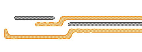
11 LELE SIT 11 DETAILS OF DOUBLE PATTERNING FOR METAL1X 20nm SOC opened TEOS hardmask TiN hardmask SOC opened TiN hardmask Litho1 + trilayer etch Litho1 + trilayer etch SiO2 spacer on SOC Etch TEOS hardmask Spacer Dep + Etch+ SOC strip Litho2 + trilayer etch Litho2 + trilayer etch Etch2 TEOS hardmask + TiN + resist strip Etch TiN hardmask + SOC strip Similar flow complexity, but different patterning accuracy

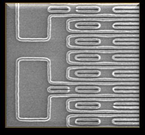
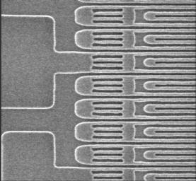


12 12 DOUBLE PATTERNING FOR METAL1X 20nm: SIT process scheme clips 3. 2 nd Block litho 4. Etch TiN HM 1. Core-mandrel 2. Spacer etch


 = 25.")
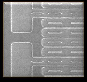
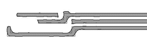
13 13 DOUBLE PATTERNING FOR METAL1X 20nm: LELE process scheme clips M1 M1+I1 I1 TEOS Hard Mask opened TEOS Hard Mask M1 TiN Hard Mask opened I1 M1 M1 TEOS Hard Mask opened TiN Hard Mask Bottom CD1(M1) = 25.7nm Bottom CD2(I1) = 27.2nm
14 14 OUTLINE Lithography Roadmap Double Patterning introduction in 45 and 28nm Technologies Double Patterning for 20nm Presentation of Double Patterning for Metal1X Interconnection for 20nm Design Challenges Process Challenges Double Patterning Costs comparison Conclusions
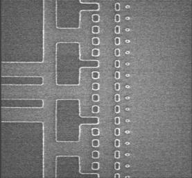
15 15 DESIGN CHALLENGES Main Challenges Need design process co-optimisation to define the rules Design rules needs to be DP-aware to avoid coloring conflict (Not able to correct these conflicts at process level). RX PC CTC > crit pitch < crit pitch < crit pitch Decomposition capability has to move from process level () to design level (P&R) P&R tools need to be abble to automaticaly correct colouring conflict

16 16 DESIGN CHALLENGES Example of DPT Routing issue SIT LELE Coloring conflict Color conflict at stitching area


17 17 DESIGN CHALLENGES After re-routing SIT LELE
18 18 OUTLINE Lithography Roadmap Double Patterning introduction in 45 and 28nm Technologies Double Patterning for 20nm Presentation of Double Patterning for Metal1X Interconnection for 20nm Design Challenges Process Challenges Double Patterning Costs comparison Conclusions

19 LELE Litho1 Litho2 PROCESS CHALLENGES LELE Overlay Litho2-litho1 CD1 CD2 Dimensional control: 2 independent distributions High dimentional control required Yield/Reliability: space between metal lines should not be too small and directly depends on overlay of litho2 to litho1 Overlay: control to previous and following double patterning levels. Gaps between lines end, have limited resolution High overlay constraint around 3 nm between litho 1 and 2 Complexe and tighter overlay to previous and following double patterning levels. Additional cut mask can be added at the expense of high costs 19


20 SIT PROCESS CHALLENGES SIT CD1 CD2 Dimensional control: CD2 depends on CD1 and uniformity of spacer process Gaps between lines end, and line to line end, is controled by the second litho High uniformity of spacer process (spacer deposition and etch) is required CD compensation from non uniformity can be optimized in litho High resolution of second litho is required for gap, through lithography and optimization 20
21 21 OUTLINE Lithography Roadmap Double Patterning introduction in 45 and 28nm Technologies Double Patterning for 20nm Presentation of Double Patterning for Metal1X Interconnection for 20nm Design Challenges Process Challenges Double Patterning Costs comparison Conclusions
22 DOUBLE PATTERNING COSTS COMPARISON 22 Back end choosen here is an 11 metal levels, using trench first hard mask for all levels but the last 2 metals, with: 2 or 3 Metal1X pitch 64: LELE or SIT using trilayer 4 or 5 Metal1X pitch 80: Single patterning using Barc 2 Metals2X 193nm lithography 2 Metals 8X 248nm lithography Pads 248nm lithography
23 23 DOUBLE PATTERNING COSTS COMPARISON 1 Metal1X brick Double Cu damascene, trench first hard mask process # Steps for Critical Met1X patterning Ref 28nm LELE SIT ULK stack deposition Hard masks dep Critical diel deposition Litho (metal+via) Etch/cleans (metal+via) Metal barrier+fill CMP # of steps Number of steps increased equally by 40%, for LELE and SIT 1


24 24 DOUBLE PATTERNING COSTS COMPARISON Cost increase for 1 Metal1X brick Cost increase for the whole Back End As a conclusion, LELE has a slight cost advantage vs SIT. It is simpler to introduce, using more conventional design rules and routers, deposition and patterning techniques, whereas it has strong overlay constraints.
25 25 OUTLINE Lithography Roadmap Double Patterning introduction in 45 and 28nm Technologies Double Patterning for 20nm Presentation of Double Patterning for Metal1X Interconnection for 20nm Design Challenges Process Challenges Double Patterning Costs comparison Conclusions
26 26 CONCLUSIONS 20nm LITHOGRAPHY LEVEL DOUBLE PATTERNING CUT MASK DOUBLE PATTERNING PITCH SPLIT - LELE DOUBLE PATTERNING PITCH DOUBLING - SIT ACTIVE - GATE -Possible strategy because of 80nm -Process: overlay not over constrained -Cost: low added cost -Possible strategy -Process: high overlay constraint -Cost: moderate added cost -Possible strategy -Process: constraint on CD control -Cost: moderate added cost CONTACT VIA1X -Not suitable! Possible strategy Process: overlay not overconstrained if contact is the only LELE level -Possible, with very restrictive design rules LINE1X -Impossible due to pitch < 80nm -Possible strategy -Design: easy for traditional routing tools -Process: high overlay constraint -Cost: moderate added cost -Possible strategy -Design: need new routing tools -Process: need new critical deposition process. Constraint on CD control. Scalable down to 14nm. -Cost: moderate added cost
27 27 Acknowledgements This presentation has been made possible thanks To Lens Project Organisation and Partners To ST R&D teams

28 Thank You 28
Self-Aligned Double Patterning for 3xnm Flash Production
 Self-Aligned Double Patterning for 3xnm Flash Production Chris Ngai Dir of Process Engineering & Lithography Maydan Technology Center Group Applied Materials, Inc. July 16 th, 2008 Overview Double Patterning
COMPARISON OF EUV SINGLE EXPOSURE VS. 193i MULTIPLE PATTERING FOR N10 BEOL CHRISTOPHER J. WILSON
 COMPARISON OF EUV SINGLE EXPOSURE VS. 193i MULTIPLE PATTERING FOR N10 BEOL CHRISTOPHER J. WILSON - CONTRIBUTORS FORM ADVANCED LITHO AND CU-LOW-K IIAP PROGRAMS - ASML VELDHOVEN DEMO LAB FOR EXPOSURES EUV
Outline. Double Patterning 11/6/17. Motivation Techniques Future of Double Patterning. Rasha El-Jaroudi November 7 th
 Double Patterning Rasha El-Jaroudi November 7 th 2017 reljaroudi@utexas.edu Outline Motivation Techniques Future of Double Patterning Rasha H. El-Jaroudi 2 1 Motivation Need to keep up with Moore s Law
SEMICON Europe October Pushing Lithography to the Limits. Patrick Wong imec
 SEMICON Europe October 2009 Pushing Lithography to the Limits imec 2009 1 Alternative double patterning processes : ready for (sub) 32nm hp? P. Wong, M. Maenhoudt, D. Vangoidsenhoven, V. Wiaux Outline
Because Innovation Matters
 Because Innovation Matters Silicon Systems Group Toru Watanabe President, Applied Materials, Japan Semicon Japan November 30, 2010 Safe Harbor This presentation contains forward-looking statements, including
Double Patterning OPC and Design for 22nm to 16nm Device Nodes
 Double Patterning OPC and Design for 22nm to 16nm Device Nodes Kevin Lucas, Chris Cork, Alex Miloslavsky, Gerry Luk-Pat, Xiaohai Li, Levi Barnes, Weimin Gao Synopsys Inc. Vincent Wiaux IMEC 1 Outline Introduction
Overcoming Challenges in 3D NAND Volume Manufacturing
 Overcoming Challenges in 3D NAND Volume Manufacturing Thorsten Lill Vice President, Etch Emerging Technologies and Systems Flash Memory Summit 2017, Santa Clara 2017 Lam Research Corp. Flash Memory Summit
Nano-Imprint Lithography Infrastructure: Imprint Templates
 Nano-Imprint Lithography Infrastructure: Imprint Templates John Maltabes Photronics, Inc Austin, TX 1 Questions to keep in mind Imprint template manufacturability Resolution Can you get sub30nm images?
Readiness and Challenges of EUV Mask
 Panel Discussion: EUVL HVM Insertion and Scaling Readiness and Challenges of EUV Mask Takashi Kamo Toshiba Corporation Semiconductor & Storage Products Company Contents [1] Introduction [2] EUV Mask Defect
Post-Routing Layer Assignment for Double Patterning
 Post-Routing Layer Assignment for Double Patterning Jian Sun 1, Yinghai Lu 2, Hai Zhou 1,2 and Xuan Zeng 1 1 Micro-Electronics Dept. Fudan University, China 2 Electrical Engineering and Computer Science
ADVANCED MICRO DEVICES, 2 CADENCE DESIGN SYSTEMS
 METHODOLOGY FOR ANALYZING AND QUANTIFYING DESIGN STYLE CHANGES AND COMPLEXITY USING TOPOLOGICAL PATTERNS JASON CAIN 1, YA-CHIEH LAI 2, FRANK GENNARI 2, JASON SWEIS 2 1 ADVANCED MICRO DEVICES, 2 CADENCE
1. Publishable summary
 1. Publishable summary 1.1. Project objectives. The target of the project is to develop a highly reliable high brightness conformable low cost scalable display for demanding applications such as their
UV Nanoimprint Tool and Process Technology. S.V. Sreenivasan December 13 th, 2007
 UV Nanoimprint Tool and Process Technology S.V. Sreenivasan December 13 th, 2007 Agenda Introduction Need tool and process technology that can address: Patterning and CD control Alignment and Overlay Defect
Approaching Zero Etch Bias at Cr Etch Process
 Approaching Zero Etch Bias at Cr Etch Process Pavel Nesladek a ; Norbert Falk b ; Andreas Wiswesser a ; Renee Koch b ; Björn Sass a a Advanced Mask Technology Center, Rähnitzer Allee 9; 01109 Dresden,
Patterning Challenges for N7 and Beyond At a Crossroads. Steven Scheer. Director, Corporate Development Division TOKYO ELECTRON LIMITED
 Patterning Challenges for N7 and Beyond At a Crossroads Steven Scheer Director, Corporate Development Division TOKYO ELECTRON LIMITED Advanced Technologies in Accelerating Digital Era and IoT Forum Friday,
Next Generation of Poly-Si TFT Technology: Material Improvements and Novel Device Architectures for System-On-Panel (SOP)
") Next Generation of Poly-Si TFT Technology: Material Improvements and Novel Device Architectures for System-On-Panel (SOP) Tolis Voutsas* Paul Schuele* Bert Crowder* Pooran Joshi* Robert Sposili* Hidayat
Next Generation of Poly-Si TFT Technology: Material Improvements and Novel Device Architectures for System-On-Panel (SOP) Tolis Voutsas* Paul Schuele* Bert Crowder* Pooran Joshi* Robert Sposili* Hidayat
SEMICONDUCTOR TECHNOLOGY -CMOS-
 SEMICONDUCTOR TECHNOLOGY -CMOS- Fire Tom Wada 2011/12/19 1 What is semiconductor and LSIs Huge number of transistors can be integrated in a small Si chip. The size of the chip is roughly the size of nails.
Digital Light Processing
 A Seminar report On Digital Light Processing Submitted in partial fulfillment of the requirement for the award of degree of Bachelor of Technology in Computer Science SUBMITTED TO: www.studymafia.org SUBMITTED
Possible Paths for Cu CMP
 Possible Paths for Cu CMP J.S. Drewery, V. Hardikar, S.T. Mayer, H. Meinhold, F. Juarez, and J. Svirchevski Presented by Julia Svirchevski Agenda Perceived Need for ECMP Technology Differentiation Profile
Recent results of Multi-beam mask writer MBM-1000
 Recent results of Multi-beam mask writer MBM-1000 Hiroshi Matsumoto, Hiroshi Yamashita, Hideo Inoue, Kenji Ohtoshi, Hirokazu Yamada Member of the ebeam Initiative 1 NFT s mask writer roadmap 2016 Device
SEMICONDUCTOR TECHNOLOGY -CMOS-
 SEMICONDUCTOR TECHNOLOGY -CMOS- Fire Tom Wada What is semiconductor and LSIs Huge number of transistors can be integrated in a small Si chip. The size of the chip is roughly the size of nails. Currently,
The Challenges in Making NIL Master Templates
 The Challenges in Making NIL Master Templates Naoya Hayashi Dai Nippon Printing Co., Ltd. A Member of the ebeam Initiative 2011 Dai Nippon Printing Co.,Ltd. All Rights Reserved. OUTLINE Recent Progress
Scan Chain and Power Delivery Network Synthesis for Pre-Bond Test of 3D ICs
 Die 1 Die 0 Scan Chain and Power Delivery Network Synthesis for Pre-Bond Test of 3D ICs Shreepad Panth and Sung Kyu Lim School of Electrical and Computer Engineering Georgia Institute of Technology Email:
Applied Materials. 200mm Tools & Process Capabilities For Next Generation MEMS. Dr Michel (Mike) Rosa
 Rosa") Applied Materials 200mm Tools & Process Capabilities For Next Generation MEMS Dr Michel (Mike) Rosa 200mm MEMS Global Product / Marketing Manager, Components and Systems Group (CSG), Applied Global Services
Applied Materials 200mm Tools & Process Capabilities For Next Generation MEMS Dr Michel (Mike) Rosa 200mm MEMS Global Product / Marketing Manager, Components and Systems Group (CSG), Applied Global Services
Sharif University of Technology. SoC: Introduction
 SoC Design Lecture 1: Introduction Shaahin Hessabi Department of Computer Engineering System-on-Chip System: a set of related parts that act as a whole to achieve a given goal. A system is a set of interacting
The Transition to Patterned Media in Hard Disk Drives
 The Transition to Patterned Media in Hard Disk Drives The Evolution of Jet and Flash Imprint Lithography for Patterned Media DISKCON San Jose Sept 24 rd, 2009 Paul Hofemann, Vice President, HDD Future
AltiumLive 2017: Effective Methods for Advanced Routing
 AltiumLive 2017: Effective Methods for Advanced Routing Charles Pfeil Senior Product Manager Dave Cousineau Sr. Field Applications Engineer Charles Pfeil Senior Product Manager Over 50 years of experience
Advances in Roll-to-Roll Imprint Lithography for Display Applications Using Self Aligned Imprint Lithography. John G Maltabes HP Labs
 Advances in Roll-to-Roll Imprint Lithography for Display Applications Using Self Aligned Imprint Lithography John G Maltabes HP Labs Outline Introduction Roll to Roll Challenges and Benefits HP Labs Roll
Defect Reduction for Semiconductor Memory Applications Using Jet And Flash Imprint Lithography
 Defect Reduction for Semiconductor Memory Applications Using Jet And Flash Imprint Lithography Zhengmao Ye, Kang Luo, Xiaoming Lu, Brian Fletcher, Weijun Liu, Frank Xu, Dwayne LaBrake, Douglas Resnick,
Introduction and recent results of Multi-beam mask writer MBM-1000
 Introduction and recent results of Multi-beam mask writer MBM-1000 Hiroshi Matsumoto, Yasuo Kato, Munehiro Ogasawara, Hirokazu Yamada February 23 rd, 2016 Member of the ebeam Initiative NFT s mask writer
Selective isotropic etching of Group IV semiconductors to enable gate all around device architectures
 TEL Technology Center, America, LLC - imec Selective isotropic etching of Group IV semiconductors to enable gate all around device architectures SPCC, April 10, 2018 S. Kal 1, C. Pereira 1, Y. Oniki 2,
How UV selectable illumination inspection tool and methodologies can accelerate learning curve of advanced technologies
 How UV selectable illumination inspection tool and methodologies can accelerate learning curve of advanced technologies V. Twines, C. Archambuult, B. Hinschberger, E. Rouchouze ST Microelectronic Crolles
Asynchronous IC Interconnect Network Design and Implementation Using a Standard ASIC Flow
 Asynchronous IC Interconnect Network Design and Implementation Using a Standard ASIC Flow Bradley R. Quinton*, Mark R. Greenstreet, Steven J.E. Wilton*, *Dept. of Electrical and Computer Engineering, Dept.
Transforming Electronic Interconnect Breaking through historical boundaries Tim Olson Founder & CTO
 Transforming Electronic Interconnect Breaking through historical boundaries Tim Olson Founder & CTO Remember when? There were three distinct industries Wafer Foundries SATS EMS Semiconductor Devices Nanometers
Pre SiGe Wet Cleans Development for sub 1x nm Technology Node
 Pre SiGe Wet Cleans Development for sub 1x nm Technology Node Akshey Sehgal, Anand Kadiyala, Michael DeVre and, Norberto Oliveria April 10 th, 2018 Background Due to higher aspect ratio features observed
Advanced Display Manufacturing Technology
 Advanced Display Manufacturing Technology John Busch Vice President, New Business Development Display and Flexible Technology Group September 28, 2017 Safe Harbor This presentation contains forward-looking
Leveraging 300 mm Technology Solutions to Enable New MEMS Process Capabilities
 Leveraging 300 mm Technology Solutions to Enable New MEMS Process Capabilities Evan Patton Semicon Europa November 2017 Lam Research Corp. 1 Presentation Outline The Internet of Things (IoT) as a market
High Performance Microprocessor Design and Automation: Overview, Challenges and Opportunities IBM Corporation
 High Performance Microprocessor Design and Automation: Overview, Challenges and Opportunities Introduction About Myself What to expect out of this lecture Understand the current trend in the IC Design
PROGRESS OF UV-NIL TEMPLATE MAKING
 PROGRESS OF UV-NIL TEMPLATE MAKING Takaaki Hiraka, Jun Mizuochi, Yuko Nakanishi, Satoshi Yusa, Shiho Sasaki, Yasutaka Morikawa, Hiroshi Mohri, and Naoya Hayashi Electronic Device Laboratory, Dai Nippon
Inspection of 32nm imprinted patterns with an advanced e-beam inspection system
 Inspection of 32nm imprinted patterns with an advanced e-beam inspection system Hong Xiao, Long (Eric) Ma, Fei Wang, Yan Zhao, and Jack Jau Hermes Microvision, Inc., 1762 Automation Parkway, San Jose,
Automotive Display. Technology & Products. Truly Automotive Display Department Rev. K
 Automotive Display Technology & Products Truly Automotive Display Department Rev. K Content: Technology I: mature products, such as TN, ETN, FSTN, WSTN, ESTN, DSTN, ASTN Technology II: new products 1.
QUIZ BUZZER KIT TEACHING RESOURCES. Version 2.0 WHO ANSWERED FIRST? FIND OUT WITH THIS
 TEACHING RESOURCES SCHEMES OF WORK DEVELOPING A SPECIFICATION COMPONENT FACTSHEETS HOW TO SOLDER GUIDE WHO ANSWERED FIRST? FIND OUT WITH THIS QUIZ BUZZER KIT Version 2.0 Index of Sheets TEACHING RESOURCES
Phosphorescent OLED Technologies: The Next Wave. Plastic Electronics Conference Oct 9, 2012
 Phosphorescent OLED Technologies: The Next Wave Plastic Electronics Conference Oct 9, 2012 UDC Company Focus IP innovator, technology developer, patent licensor and materials supplier for the rapidly growing
Fabrication of Step and Flash TM Imprint Lithography Templates Using Commercial Mask Processes
 Fabrication of Step and Flash TM Imprint Lithography Templates Using Commercial Mask Processes Ecron Thompson, Peter Rhyins, Ron Voisin, S.V. Sreenivasan *, Patrick Martin Molecular Imprints, Inc., 1807C
Study of Pattern Area Reduction. with FinFET and SGT for LSI
 Contemporary Engineering Sciences, Vol. 6, 2013, no. 4, 177-190 HIKRI Ltd, www.m-hikari.com Study of Pattern rea Reduction with FinFET and SGT for LSI Takahiro Kodama Japan Process Development Co., Ltd.
Overview of All Pixel Circuits for Active Matrix Organic Light Emitting Diode (AMOLED)
") Chapter 2 Overview of All Pixel Circuits for Active Matrix Organic Light Emitting Diode (AMOLED) ---------------------------------------------------------------------------------------------------------------
Chapter 2 Overview of All Pixel Circuits for Active Matrix Organic Light Emitting Diode (AMOLED) ---------------------------------------------------------------------------------------------------------------
The Impact of Device-Width Quantization on Digital Circuit Design Using FinFET Structures
 EE 241 SPRING 2004 1 The Impact of Device-Width Quantization on Digital Circuit Design Using FinFET Structures Farhana Sheikh, Vidya Varadarajan {farhana, vidya}@eecs.berkeley.edu Abstract FinFET structures
IC Mask Design. Christopher Saint Judy Saint
 IC Mask Design Essential Layout Techniques Christopher Saint Judy Saint McGraw-Hill New York Chicago San Francisco Lisbon London Madrid Mexico City Milan New Delhi San Juan Seoul Singapore Sydney Toronto
Development of OLED Lighting Applications Using Phosphorescent Emission System
 Development of OLED Lighting Applications Using Phosphorescent Emission System Kazuhiro Oikawa R&D Department OLED Lighting Business Center KONICA MINOLTA ADVANCED LAYERS, INC. October 10, 2012 Outline
Addressing 80 µm pitch Cu Pillar Bump Wafer probing: Technoprobe TPEG MEMS solution
 Addressing 80 µm pitch Cu Pillar Bump Wafer probing: Technoprobe TPEG MEMS solution S. Angles STMicroelectronics R. Vallauri Technoprobe Background Overview ST Qualification of TPEG MEMS T3 probing technology
Multi-Shaped E-Beam Technology for Mask Writing
 Multi-Shaped E-Beam Technology for Mask Writing Juergen Gramss a, Arnd Stoeckel a, Ulf Weidenmueller a, Hans-Joachim Doering a, Martin Bloecker b, Martin Sczyrba b, Michael Finken b, Timo Wandel b, Detlef
Semiconductors Displays Semiconductor Manufacturing and Inspection Equipment Scientific Instruments
 Semiconductors Displays Semiconductor Manufacturing and Inspection Equipment Scientific Instruments Electronics 110-nm CMOS ASIC HDL4P Series with High-speed I/O Interfaces Hitachi has released the high-performance
IC TECHNOLOGY Lecture 2.
 IC TECHNOLOGY Lecture 2. IC Integrated Circuit Technology Integrated Circuit: An integrated circuit (IC, a chip, or a microchip) is a set of electronic circuits on one small flat piece (or "chip") of semiconductor
3M High-Speed Solutions
 3M High-Speed Solutions 3M 2011. All Rights Reserved. Distance 3M Electronic Solutions Division 3M Twin Axial and AOC Solutions Addressing Physical Medium Dependent in the InifiniBand Fabric 100m 10m 1m
Challenges for OLED Deposition by Vacuum Thermal Evaporation. D. W. Gotthold, M. O Steen, W. Luhman, S. Priddy, C. Counts, C.
 Challenges for OLED Deposition by Vacuum Thermal Evaporation D. W. Gotthold, M. O Steen, W. Luhman, S. Priddy, C. Counts, C. Roth June 7, 2011 Outline Introduction to Veeco Methods of OLED Deposition Cost
FinFETs & SRAM Design
 FinFETs & SRAM Design Raymond Leung VP Engineering, Embedded Memories April 19, 2013 Synopsys 2013 1 Agenda FinFET the Device SRAM Design with FinFETs Reliability in FinFETs Summary Synopsys 2013 2 How
MEMS Technologies Dresden - Product Development and Fabrication at IPMS Dresden
 MEMS Technologies Dresden - Product Development and Fabrication at IPMS Dresden MEMS Technologies Dresden - Product Development and Fabrication at IPMS Dresden Michael Müller, Matthias List Outline FhG-IPMS
Methodology for Trench Capacitor Etch Optimization using Voltage Contrast Inspection and Special Processing
 Methodology for Trench Capacitor Etch Optimization using Voltage Contrast Inspection and Special Processing 1 Oliver D. Patterson, 1 Xing J. Zhou, 1 Rohit S. Takalkar, 1 Katherine V. Hawkins, 1 Eric H.
PROCEEDINGS OF SPIE. Classification and printability of EUV mask defects from SEM images
 PROCEEDINGS OF SPIE SPIEDigitalLibrary.org/conference-proceedings-of-spie Classification and printability of EUV mask defects from SEM images Wonil Cho, Daniel Price, Paul A. Morgan, Daniel Rost, Masaki
Scalable self-aligned active matrix IGZO TFT backplane technology and its use in flexible semi-transparent image sensors. Albert van Breemen
 Scalable self-aligned active matrix IGZO TFT backplane technology and its use in flexible semi-transparent image sensors Albert van Breemen Image sensors today 1 Dominated by silicon based technology on
Through Silicon Via Testing Known Good Die (KGD) or Probably Good Die (PGD) Doug Lefever Advantest
 or Probably Good Die (PGD) Doug Lefever Advantest") Through Silicon Via Testing Known Good Die (KGD) or Probably Good Die (PGD) Doug Lefever Advantest Single Die Fab Yield will drive Cost Equation. Yield of the device to be stacked 100% 90% 80% Yield of
Through Silicon Via Testing Known Good Die (KGD) or Probably Good Die (PGD) Doug Lefever Advantest Single Die Fab Yield will drive Cost Equation. Yield of the device to be stacked 100% 90% 80% Yield of
ECE 555 DESIGN PROJECT Introduction and Phase 1
 March 15, 1998 ECE 555 DESIGN PROJECT Introduction and Phase 1 Charles R. Kime Dept. of Electrical and Computer Engineering University of Wisconsin Madison Phase I Due Wednesday, March 24; One Week Grace
This paper is a preprint of a paper accepted by Electronics Letters and is subject to Institution of Engineering and Technology Copyright.
 This paper is a preprint of a paper accepted by Electronics Letters and is subject to Institution of Engineering and Technology Copyright. The final version is published and available at IET Digital Library
FLEX2017 June, Monterey, USA Dr Mike Cowin, CMO, SmartKem.
 FLEX2017 June, Monterey, USA Dr Mike Cowin, CMO, SmartKem. FLEX2017 June, Monterey, USA Dr Mike Cowin, CMO, SmartKem. EU H2020 FLEXTRANs Grant Objectives A 24 month project (started September 2016) (Grant
CS/EE 6710 Digital VLSI Design CAD Assignment #3 Due Thursday September 21 st, 5:00pm
 CS/EE 6710 Digital VLSI Design CAD Assignment #3 Due Thursday September 21 st, 5:00pm Overview: In this assignment you will design a register cell. This cell should be a single-bit edge-triggered D-type
PHYSICAL DESIGN ESSENTIALS An ASIC Design Implementation Perspective
 PHYSICAL DESIGN ESSENTIALS An ASIC Design Implementation Perspective PHYSICAL DESIGN ESSENTIALS An ASIC Design Implementation Perspective Khosrow Golshan Conexant Systems, Inc. 1 3 Khosrow Golshan Conexant
STMicroelectronics Standard Technology offers at CMP in 2017 Deep Sub-Micron, SOI and SiGe Processes
 STMicroelectronics Standard Technology offers at CMP in 2017 Deep Sub-Micron, SOI and SiGe Processes http://cmp.imag.fr STMicroelectronics Technology offers at CMP: 160nm CMOS: BCD8SP 1994 at CMP 160nm
Abstract. Keywords INTRODUCTION. Electron beam has been increasingly used for defect inspection in IC chip
 Abstract Based on failure analysis data the estimated failure mechanism in capacitor like device structures was simulated on wafer in Front End of Line. In the study the optimal process step for electron
ESE534: Computer Organization. Previously. Today. Previously. Today. Preclass 1. Instruction Space Modeling
 ESE534: Computer Organization Previously Instruction Space Modeling Day 15: March 24, 2014 Empirical Comparisons Previously Programmable compute blocks LUTs, ALUs, PLAs Today What if we just built a custom
Deep Silicon Etch Technology for Advanced MEMS Applications
 Deep Silicon Etch Technology for Advanced MEMS Applications Shenjian Liu, Ph.D. Managing Director, AMEC AMEC Company Profile and Product Line-up AMEC HQ, R&D and MF Facility in Shanghai AMEC Taiwan AMEC
Scalable Media Systems using SMPTE John Mailhot November 28, 2018 GV-EXPO
 Scalable Media Systems using SMPTE 2110 John Mailhot November 28, 2018 SMPTE @ GV-EXPO SMPTE 2110 is mostly finished and published!!! 2110-10: System Timing PUBLISHED 2110-20: Uncompressed Video PUBLISHED
Auto classification and simulation of mask defects using SEM and CAD images
 Auto classification and simulation of mask defects using SEM and CAD images Tung Yaw Kang, Hsin Chang Lee Taiwan Semiconductor Manufacturing Company, Ltd. 25, Li Hsin Road, Hsinchu Science Park, Hsinchu
Layers of Innovation: How Signal Chain Innovations are Creating Analog Opportunities in a Digital World
 The World Leader in High Performance Signal Processing Solutions Layers of Innovation: How Signal Chain Innovations are Creating Analog Opportunities in a Digital World Dave Robertson-- VP of Analog Technology
EUV Blank Inspection
 EUV Blank Inspection J.H. Peters* a, C. Tonk a, D. Spriegel b, Hak-Seung Han c, Wonil Cho c, Stefan Wurm d a Advanced Mask Technology Center, Raehnitzer Allee 9, 01109 Dresden, Germany; b Siemens AG, Corporate
Reading a GEM with a VLSI pixel ASIC used as a direct charge collecting anode. R.Bellazzini - INFN Pisa. Vienna February
 Reading a GEM with a VLSI pixel ASIC used as a direct charge collecting anode Ronaldo Bellazzini INFN Pisa Vienna February 16-21 2004 The GEM amplifier The most interesting feature of the Gas Electron
Introducing The ebeam Initiative
 Introducing The ebeam Initiative 20 Charter Members & Advisors Across the Ecosystem Jan Willis ebeam Initiative Facilitator Member Companies & Advisors www.ebeam.org Marty Deneroff D. E. Shaw Research
21 rue La Noue Bras de Fer Nantes - France Phone : +33 (0) website :
 website :") 21 rue La Noue Bras de Fer - 44200 Nantes - France Phone : +33 (0) 240 180 916 - email : info@systemplus.fr - website : www.systemplus.fr 2012 September - Version 1 Written by: Maher Sahmimi DISCLAIMER
21 rue La Noue Bras de Fer - 44200 Nantes - France Phone : +33 (0) 240 180 916 - email : info@systemplus.fr - website : www.systemplus.fr 2012 September - Version 1 Written by: Maher Sahmimi DISCLAIMER
Chapter 05: Basic Processing Units Control Unit Design Organization. Lesson 11: Multiple Bus Organisation
 Chapter 05: Basic Processing Units Control Unit Design Organization Lesson 11: Multiple Bus Organisation Objective Understand multiple bus organisation Learn how the number of independent steps can be
Freescale SPC5604BF1CLL6 Embedded NOR Flash with M27V Die Markings 32 Bit Power Architecture Automotive Microcontroller 90 nm Logic Process
 Freescale SPC5604BF1CLL6 Embedded NOR Flash with M27V Die Markings 32 Bit Power Architecture Automotive Microcontroller 90 nm Logic Process Process Review 3685 Richmond Road, Suite 500, Ottawa, ON K2H
projectors, head mounted displays in virtual or augmented reality use, electronic viewfinders
 Beatrice Beyer Figure 1. (OLED) microdisplay with a screen diagonal of 16 mm. Figure 2. CMOS cross section with OLED on top. Usually as small as fingernails, but of very high resolution Optical system
CS250 VLSI Systems Design
 CS250 VLSI Systems Design Fall 2012 John Wawrzynek, Jonathan Bachrach with Krste Asanovic, John Lazzaro and Rimas Avizienis (TA) Why CS250 and not EE250 Put IC design expertise into the hands of those
LEP400 Etch Depth Monitor Real-time, in-situ plasma etch depth monitoring and end point control plus co-linear wafer vision system
 LEP400 Etch Depth Monitor Real-time, in-situ plasma etch depth monitoring and end point control plus co-linear wafer vision system Base Configuration Etch Depth Monitoring LEP400 Recessed Window Plasma
COLOUR CHANGING USB LAMP KIT
 TEACHING RESOURCES SCHEMES OF WORK DEVELOPING A SPECIFICATION COMPONENT FACTSHEETS HOW TO SOLDER GUIDE SEE AMAZING LIGHTING EFFECTS WITH THIS COLOUR CHANGING USB LAMP KIT Version 2.1 Index of Sheets TEACHING
RFSOI and FDSOI enabling smarter and IoT applications. Kirk Ouellette Digital Products Group STMicroelectronics
 RFSOI and FDSOI enabling smarter and IoT applications Kirk Ouellette Digital Products Group STMicroelectronics ST in the IoT already Today 2 Kirk Ouellette More then Moore Workshop - Shanghai - March 17,
TKK S ASIC-PIIRIEN SUUNNITTELU
 Design TKK S-88.134 ASIC-PIIRIEN SUUNNITTELU Design Flow 3.2.2005 RTL Design 10.2.2005 Implementation 7.4.2005 Contents 1. Terminology 2. RTL to Parts flow 3. Logic synthesis 4. Static Timing Analysis
Design and Implementation of FPGA Configuration Logic Block Using Asynchronous Static NCL
 Design and Implementation of FPGA Configuration Logic Block Using Asynchronous Static NCL Indira P. Dugganapally, Waleed K. Al-Assadi, Tejaswini Tammina and Scott Smith* Department of Electrical and Computer
nmos transistor Basics of VLSI Design and Test Solution: CMOS pmos transistor CMOS Inverter First-Order DC Analysis CMOS Inverter: Transient Response
 nmos transistor asics of VLSI Design and Test If the gate is high, the switch is on If the gate is low, the switch is off Mohammad Tehranipoor Drain ECE495/695: Introduction to Hardware Security & Trust
Antenna: a key enabler for 5G innovative RFIC development
 Forum for Electromagnetic Research Methods and Application Technologies (FERMAT) Antenna: a key enabler for 5G innovative RFIC development By Dr Fred Gianesello STMicroelectronics, Technology R&D, Silicon
P802.3av interim, Shanghai, PRC
 P802.3av interim, Shanghai, PRC 08 09.06.2009 Overview of 10G-EPON compiled by Marek Hajduczenia marek.hajduczenia@zte.com.cn Rev 1.2 P802.3av interim, Shanghai, PRC 08 09.06.2009 IEEE P802.3av 10G-EPON
SEMI 大半导体产业网
 STATE-OF-THE-ART 3D INTEGRATION GAN HUI, STEVEN OUTLINE Introduction about IMEC Application Areas Driven 3D Integration 3D Integration Technology Conclusions 1 IMEC 1984 2010 1984 Established by state
Advanced backlights for LCD cockpit displays
 Advanced backlights for LCD cockpit displays Jaap Groeneweg (NLR) Stefan Carton (NDF) 21 st April, 2016 Introduction NLR NLR = Netherlands Aerospace Centre NLR contributes key technological and scientific
ISPD 2015 Detailed Routing-Driven Placement Contest with Fence Regions and Routing Blockages
 ISPD 2015 Detailed Routing-Driven Placement Contest with Fence Regions and Routing Blockages Ismail Bustany David Chinnery Joseph Shinnerl Vladimir Yutsis www.ispd.cc/contests/15/ispd2015_contest.html
data and is used in digital networks and storage devices. CRC s are easy to implement in binary
 Introduction Cyclic redundancy check (CRC) is an error detecting code designed to detect changes in transmitted data and is used in digital networks and storage devices. CRC s are easy to implement in
NZQA registered unit standard version 1 Page 1 of 6. Prepare and write a news story for broadcast on television
 Page 1 of 6 Title Prepare and write a news story for broadcast on television Level 5 Credits 5 Purpose This unit standard is intended for people studying journalism in an off-job situation. People credited
Reconfigurable Neural Net Chip with 32K Connections
 Reconfigurable Neural Net Chip with 32K Connections H.P. Graf, R. Janow, D. Henderson, and R. Lee AT&T Bell Laboratories, Room 4G320, Holmdel, NJ 07733 Abstract We describe a CMOS neural net chip with
Lithography-Induced Limits to Scaling of Design Quality
 Lithography-Induced Limits to Scaling of Design Quality Abstract Andrew B. Kahng ECE and CSE Depts., University of California at San Diego, La Jolla, CA USA 92093 Quality and value of an IC product are
Flexible Electronics Production Deployment on FPD Standards: Plastic Displays & Integrated Circuits. Stanislav Loboda R&D engineer
 Flexible Electronics Production Deployment on FPD Standards: Plastic Displays & Integrated Circuits Stanislav Loboda R&D engineer The world-first small-volume contract manufacturing for plastic TFT-arrays
Focused-ion-beam fabrication of nanoplasmonic devices
 Focused-ion-beam fabrication of nanoplasmonic devices H. J. Lezec Center for Nanoscale Science and Technology, NIST, Gaithersburg MD, USA.. Outline 1) Plasmon-induced negative refraction at visible frequencies
AltiumLive 2017: The Benefits of Grid Systems in Board Design
 AltiumLive 2017: The Benefits of Grid Systems in Board Design Susy Webb Sr PCB Designer San Diego, CA October 3-4, 2017 The information contained herein is the opinion of the presenter and not considered
Optimizing BNC PCB Footprint Designs for Digital Video Equipment
 Optimizing BNC PCB Footprint Designs for Digital Video Equipment By Tsun-kit Chin Applications Engineer, Member of Technical Staff National Semiconductor Corp. Introduction An increasing number of video