Week 5 Dr. David Ward Hybrid Embedded Systems
|
|
|
- Doris Pope
- 5 years ago
- Views:
Transcription

1 Week 5 Dr. David Ward Hybrid Embedded Systems
2 Today s Agenda Discuss Homework and Labs HW #2 due September 24 (this Friday by midnight) Don t start Lab # 5 until next week Work on HW #2 in today s lab Project Proposal VGA Basics Verilog example Chapter 7.7 textbook SOPC Builder ftp://ftp.altera.com/up/pub/university_program_ip_cores/v GA.pdf
3
4 Proposal Each student should submit a one- or two-page written project proposal. You should crystallize the details of your project You should focus your energies on producing a high quality project The proposal should include enough detail to convince the reader that you've found a good project You understand the complexity of your project You should map out a plan for how to implement it and complete it on schedule You should have an idea about which experiments you might run to test the success of your implementation Please do not be vague in your written proposal After submitting your project proposal, schedule a half-hour meeting with instructor. If needed, we will make any adjustments in the scope or detail of your project
5 Proposal Outline Example Goal What am I going to do? Who would benefit? What will you build? What will you demonstrate? Resources What equipment/hardware and software will you require? Where and how will you get such resources Problem Statement Why is it hard? How hard is it? Previous Work What have others tried? Approach What approach am I going to try? Why do you think it will work well? What parts do you expect to be difficult, and which will be easy? Methodology What steps (task list) are required? Which of these steps is particularly hard? What to do if the hard steps don't work out? Metrics How will I measure success? Timeline Give a timeline e indicating what each group member will accomplish each week until the project is completed (from task list) I would recommend that you have a working prototype ready to demonstrate midway (week 11-12)
6 Chapter (Textbook)
7 Horizontal Synchronization
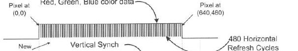
8 Vertical Synchronization
9 Character Display Hardware MonitorSynch characterpointer CharacterMatrix MaxtrixSlice characterpixel
10 MonitorSynch 800 cycles to complete Horizontal Synch
11 CharacterPointer Selects a 8x8 character (4800 total)
12 MatrixSlice Character range Flat memory 512 bytes needed to store characters
13 CharacterPixel
14 TestBench w/ DualPort RAM Can display current content while writing new data
15 Altera University IP Core


16 VGA Core Block Diagram
17 Altera VGA Core Drives Di the signals for VGADiitlt Digital-to-Analog l Converter (DAC) Horizontal and Vertical synchronization signals refresh of 60 frames/sec 25Mhz input clock Slave ports run at 50Mhz Pixel Character Supports pixel or character input Pixel l SRAM Avalon_pixel_slave Character On-chip memory Avalon_character_slave Flat contiguous memory space (simple memory interface) Can be used with other SOPC components using SOPC Builder
18 Pixel Mode User can provide the color of each pixel lto the Avalon Interface Avalon_pixel_slave Uses SRAM as pixel buffer Suitable for animation or image display Color C l Setting RGB color model 16 bit color mode Red and blue have 5-bit color spaces Green G has 6-bit color space 8-bit color mode for grayscale Resolution Supports 640x480 => 307,200 pixels Support t mega pixel for lower resolution 80 x 60. Each mega pixel is 8 x 8 pixel group 320 x 240. Each mega pixel is 2 x 2 pixel group
19 Character Mode Operates O t on characters Characters are sent to VGA Core Avalon_char_slave Handles conversion of characters to pixel Initializes I or reset tvga core to space No display Clear screen by writing 1 to highest memory location Color Setting 9-bit color mode. Each color has a 3-bit color space 8-bit color mode. 4-bit color mode 1-bit color mode. Characters are drawn in white with transparent tbackground
20 Character Size
21 Address Format

")
22 Data Format (Pixel Slave)


23 Data Format (Character)
24 SOPC Builder Instantiation
25 VGA Functions
26 RGB Color Table


27
Design and Implementation of an AHB VGA Peripheral
 Design and Implementation of an AHB VGA Peripheral 1 Module Overview Learn about VGA interface; Design and implement an AHB VGA peripheral; Program the peripheral using assembly; Lab Demonstration. System
Pivoting Object Tracking System
 Pivoting Object Tracking System [CSEE 4840 Project Design - March 2009] Damian Ancukiewicz Applied Physics and Applied Mathematics Department da2260@columbia.edu Jinglin Shen Electrical Engineering Department
Massachusetts Institute of Technology Department of Electrical Engineering and Computer Science Introductory Digital Systems Laboratory
 Problem Set Issued: March 3, 2006 Problem Set Due: March 15, 2006 Massachusetts Institute of Technology Department of Electrical Engineering and Computer Science 6.111 Introductory Digital Systems Laboratory
Lecture 14: Computer Peripherals
 Lecture 14: Computer Peripherals The last homework and lab for the course will involve using programmable logic to make interesting things happen on a computer monitor should be even more fun than the
FPGA Laboratory Assignment 4. Due Date: 06/11/2012
 FPGA Laboratory Assignment 4 Due Date: 06/11/2012 Aim The purpose of this lab is to help you understanding the fundamentals of designing and testing memory-based processing systems. In this lab, you will
Massachusetts Institute of Technology Department of Electrical Engineering and Computer Science Introductory Digital Systems Laboratory
 Problem Set Issued: March 2, 2007 Problem Set Due: March 14, 2007 Massachusetts Institute of Technology Department of Electrical Engineering and Computer Science 6.111 Introductory Digital Systems Laboratory
Lancelot. VGA video controller for the Altera Nios II processor. V4.0. December 16th, 2005
 Lancelot VGA video controller for the Altera Nios II processor. V4.0 December 16th, 2005 http://www.microtronix.com 1. Description Lancelot is a VGA video controller for the Altera Nios (II) processor.
VID_OVERLAY. Digital Video Overlay Module Rev Key Design Features. Block Diagram. Applications. Pin-out Description
 Key Design Features Block Diagram Synthesizable, technology independent VHDL IP Core Video overlays on 24-bit RGB or YCbCr 4:4:4 video Supports all video resolutions up to 2 16 x 2 16 pixels Supports any
VGA Controller. Leif Andersen, Daniel Blakemore, Jon Parker University of Utah December 19, VGA Controller Components
 VGA Controller Leif Andersen, Daniel Blakemore, Jon Parker University of Utah December 19, 2012 Fig. 1. VGA Controller Components 1 VGA Controller Leif Andersen, Daniel Blakemore, Jon Parker University
Digital Blocks Semiconductor IP
 Digital Blocks Semiconductor IP General Description The Digital Blocks IP Core decodes an ITU-R BT.656 digital video uncompressed NTSC 720x486 (525/60 Video System) and PAL 720x576 (625/50 Video System)
Lab # 9 VGA Controller
 Lab # 9 VGA Controller Introduction VGA Controller is used to control a monitor (PC monitor) and has a simple protocol as we will see in this lab. Kit parts for this lab 1 A closer look VGA Basics The
Laboratory Exercise 4
 Laboratory Exercise 4 Polling and Interrupts The purpose of this exercise is to learn how to send and receive data to/from I/O devices. There are two methods used to indicate whether or not data can be
Bitec. HSMC Quad Video Mosaic Reference Design. DSP Solutions for Industry & Research. Version 0.1
 Bitec DSP Solutions for Industry & Research HSMC Quad Video Mosaic Reference Design Version 0.1 Page 2 Revision history... 3 Introduction... 4 Installation... 5 Building the demo software... 6 Page 3 Revision
VGA 8-bit VGA Controller
 Summary This document provides detailed reference information with respect to the VGA Controller peripheral device. Core Reference CR0113 (v3.0) March 13, 2008 The VGA Controller provides a simple, 8-bit
Design and Implementation of SOC VGA Controller Using Spartan-3E FPGA
 Design and Implementation of SOC VGA Controller Using Spartan-3E FPGA 1 ARJUNA RAO UDATHA, 2 B.SUDHAKARA RAO, 3 SUDHAKAR.B. 1 Dept of ECE, PG Scholar, 2 Dept of ECE, Associate Professor, 3 Electronics,
Digital Blocks Semiconductor IP
 Digital Blocks Semiconductor IP DB3 CCIR 656 Encoder General Description The Digital Blocks DB3 CCIR 656 Encoder IP Core encodes 4:2:2 Y CbCr component digital video with synchronization signals to conform
Block Diagram. dw*3 pixin (RGB) pixin_vsync pixin_hsync pixin_val pixin_rdy. clk_a. clk_b. h_s, h_bp, h_fp, h_disp, h_line
 pixin_vsync pixin_hsync pixin_val pixin_rdy. clk_a. clk_b. h_s, h_bp, h_fp, h_disp, h_line") Key Design Features Block Diagram Synthesizable, technology independent IP Core for FPGA, ASIC and SoC reset underflow Supplied as human readable VHDL (or Verilog) source code Simple FIFO input interface
Key Design Features Block Diagram Synthesizable, technology independent IP Core for FPGA, ASIC and SoC reset underflow Supplied as human readable VHDL (or Verilog) source code Simple FIFO input interface
AD9884A Evaluation Kit Documentation
 a (centimeters) AD9884A Evaluation Kit Documentation Includes Documentation for: - AD9884A Evaluation Board - SXGA Panel Driver Board Rev 0 1/4/2000 Evaluation Board Documentation For the AD9884A Purpose
EECS150 - Digital Design Lecture 12 - Video Interfacing. Recap and Outline
 EECS150 - Digital Design Lecture 12 - Video Interfacing Oct. 8, 2013 Prof. Ronald Fearing Electrical Engineering and Computer Sciences University of California, Berkeley (slides courtesy of Prof. John
TSIU03: Lab 3 - VGA. Petter Källström, Mario Garrido. September 10, 2018
 Petter Källström, Mario Garrido September 10, 2018 Abstract In the initialization of the DE2-115 (after you restart it), an image is copied into the SRAM memory. What you have to do in this lab is to read
GENERAL RULES FOR EE314 PROJECTS
 GENERAL RULES FOR EE314 PROJECTS Followings are the important points about projects: This year we are offering 5 projects. Please note that during weekends, laboratory will be closed. In order to work
Design and implementation (in VHDL) of a VGA Display and Light Sensor to run on the Nexys4DDR board Report and Signoff due Week 6 (October 4)
 of a VGA Display and Light Sensor to run on the Nexys4DDR board Report and Signoff due Week 6 (October 4)") ECE 574: Modeling and synthesis of digital systems using Verilog and VHDL Fall Semester 2017 Design and implementation (in VHDL) of a VGA Display and Light Sensor to run on the Nexys4DDR board Report and
ECE 574: Modeling and synthesis of digital systems using Verilog and VHDL Fall Semester 2017 Design and implementation (in VHDL) of a VGA Display and Light Sensor to run on the Nexys4DDR board Report and
Design and Implementation of Nios II-based LCD Touch Panel Application System
 Design and Implementation of Nios II-based Touch Panel Application System Tong Zhang 1, Wen-Ping Ren 2, Yi-Dian Yin, and Song-Hai Zhang School of Information Science and Technology, Yunnan University No.2,
An FPGA Based Solution for Testing Legacy Video Displays
 An FPGA Based Solution for Testing Legacy Video Displays Dale Johnson Geotest Marvin Test Systems Abstract The need to support discrete transistor-based electronics, TTL, CMOS and other technologies developed
Block Diagram. pixin. pixin_field. pixin_vsync. pixin_hsync. pixin_val. pixin_rdy. pixels_per_line. lines_per_field. pixels_per_line [11:0]
![Block Diagram. pixin. pixin_field. pixin_vsync. pixin_hsync. pixin_val. pixin_rdy. pixels_per_line. lines_per_field. pixels_per_line [11:0]](/thumbs/89/100740305.jpg "Block Diagram. pixin. pixin_field. pixin_vsync. pixin_hsync. pixin_val. pixin_rdy. pixels_per_line. lines_per_field. pixels_per_line [11:0]") Rev 13 Key Design Features Block Diagram Synthesizable, technology independent IP Core for FPGA and ASIC Supplied as human readable VHDL (or Verilog) source code reset deint_mode 24-bit RGB video support
Rev 13 Key Design Features Block Diagram Synthesizable, technology independent IP Core for FPGA and ASIC Supplied as human readable VHDL (or Verilog) source code reset deint_mode 24-bit RGB video support
Block Diagram. 16/24/32 etc. pixin pixin_sof pixin_val. Supports 300 MHz+ operation on basic FPGA devices 2 Memory Read/Write Arbiter SYSTEM SIGNALS
 Key Design Features Block Diagram Synthesizable, technology independent IP Core for FPGA, ASIC or SoC Supplied as human readable VHDL (or Verilog) source code Output supports full flow control permitting
TV Character Generator
 TV Character Generator TV CHARACTER GENERATOR There are many ways to show the results of a microcontroller process in a visual manner, ranging from very simple and cheap, such as lighting an LED, to much
ANALOG TO VGA VIDEO INTERFACE GREGORY M. REDMAN. A technical report submitted to the Graduate School. In partial fulfillment of the requirements
 ANALOG TO VGA VIDEO INTERFACE BY GREGORY M. REDMAN A technical report submitted to the Graduate School In partial fulfillment of the requirements for the degree Master of Sciences, Engineering Specialization
Checkpoint 2 Video Encoder
 UNIVERSITY OF CALIFORNIA AT BERKELEY COLLEGE OF ENGINEERING DEPARTMENT OF ELECTRICAL ENGINEERING AND COMPUTER SCIENCE ASSIGNED: Week of 3/7 DUE: Week of 3/14, 10 minutes after start (xx:20) of your assigned
Digilent Nexys-3 Cellular RAM Controller Reference Design Overview
 Digilent Nexys-3 Cellular RAM Controller Reference Design Overview General Overview This document describes a reference design of the Cellular RAM (or PSRAM Pseudo Static RAM) controller for the Digilent
1 Terasic Inc. D8M-GPIO User Manual
 1 Chapter 1 D8M Development Kit... 4 1.1 Package Contents... 4 1.2 D8M System CD... 5 1.3 Assemble the Camera... 5 1.4 Getting Help... 6 Chapter 2 Introduction of the D8M Board... 7 2.1 Features... 7 2.2
VHDL Design and Implementation of FPGA Based Logic Analyzer: Work in Progress
 VHDL Design and Implementation of FPGA Based Logic Analyzer: Work in Progress Nor Zaidi Haron Ayer Keroh +606-5552086 zaidi@utem.edu.my Masrullizam Mat Ibrahim Ayer Keroh +606-5552081 masrullizam@utem.edu.my
Checkpoint 2 Video Interface
 University of California at Berkeley College of Engineering Department of Electrical Engineering and Computer Sciences EECS150 Fall 1998 R. Fearing and Kevin Cho 1. Objective Checkpoint 2 Video Interface
VGA Pixel Buffer Stephen Just
 VGA Pixel Buffer Stephen Just 2016-02-20 1 Introduction Video output is often a useful addition to interactive projects but typically there have been many performance limitations with respect to video
Bitec. HSMC DVI 1080P Colour-Space Conversion Reference Design. DSP Solutions for Industry & Research. Version 0.1
 Bitec DSP Solutions for Industry & Research HSMC DVI 1080P Colour-Space Conversion Reference Design Version 0.1 Page 2 Revision history... 3 Introduction... 4 Installation... 5 Page 3 Revision history
Design of VGA and Implementing On FPGA
 Design of VGA and Implementing On FPGA Mr. Rachit Chandrakant Gujarathi Department of Electronics and Electrical Engineering California State University, Sacramento Sacramento, California, United States
OL_H264e HDTV H.264/AVC Baseline Video Encoder Rev 1.0. General Description. Applications. Features
 OL_H264e HDTV H.264/AVC Baseline Video Encoder Rev 1.0 General Description Applications Features The OL_H264e core is a hardware implementation of the H.264 baseline video compression algorithm. The core
VGA Port. Chapter 5. Pin 5 Pin 10. Pin 1. Pin 6. Pin 11. Pin 15. DB15 VGA Connector (front view) DB15 Connector. Red (R12) Green (T12) Blue (R11)
 DB15 Connector. Red (R12) Green (T12) Blue (R11)") Chapter 5 VGA Port The Spartan-3 Starter Kit board includes a VGA display port and DB15 connector, indicated as 5 in Figure 1-2. Connect this port directly to most PC monitors or flat-panel LCD displays
Chapter 5 VGA Port The Spartan-3 Starter Kit board includes a VGA display port and DB15 connector, indicated as 5 in Figure 1-2. Connect this port directly to most PC monitors or flat-panel LCD displays
Laboratory 4. Figure 1: Serdes Transceiver
 Laboratory 4 The purpose of this laboratory exercise is to design a digital Serdes In the first part of the lab, you will design all the required subblocks for the digital Serdes and simulate them In part
Fingerprint Verification System
 Fingerprint Verification System Cheryl Texin Bashira Chowdhury 6.111 Final Project Spring 2006 Abstract This report details the design and implementation of a fingerprint verification system. The system
Laboratory 4 Check Off Sheet. Student Name: Staff Member Signature/Date: Part A: VGA Interface You must show a TA the following for check off:
 Student Name: Massachusetts Institue of Technology Department of Electrical Engineering and Computer Science 6.111 - Introductory Digital Systems Laboratory (Spring 2006) 6.111 Staff Member Signature/Date:
2.13inch e-paper HAT (D) User Manual
 User Manual") 2.13inch e-paper HAT (D) User Manual OVERVIRE This is a flexible E-Ink display HAT for Raspberry Pi, 2.13inch, 212x104 resolution, with embedded controller, communicating via SPI interface, supports partial
2.13inch e-paper HAT (D) User Manual OVERVIRE This is a flexible E-Ink display HAT for Raspberry Pi, 2.13inch, 212x104 resolution, with embedded controller, communicating via SPI interface, supports partial
Graduate Institute of Electronics Engineering, NTU Digital Video Recorder
 Digital Video Recorder Advisor: Prof. Andy Wu 2004/12/16 Thursday ACCESS IC LAB Specification System Architecture Outline P2 Function: Specification Record NTSC composite video Video compression/processing
AN-ENG-001. Using the AVR32 SoC for real-time video applications. Written by Matteo Vit, Approved by Andrea Marson, VERSION: 1.0.0
 Written by Matteo Vit, R&D Engineer Dave S.r.l. Approved by Andrea Marson, CTO Dave S.r.l. DAVE S.r.l. www.dave.eu VERSION: 1.0.0 DOCUMENT CODE: AN-ENG-001 NO. OF PAGES: 8 AN-ENG-001 Using the AVR32 SoC
Block Diagram. deint_mode. line_width. log2_line_width. field_polarity. mem_start_addr0. mem_start_addr1. mem_burst_size.
 Key Design Features Block Diagram Synthesizable, technology independent IP Core for FPGA, ASIC and SoC Supplied as human readable VHDL (or Verilog) source code pixin_ pixin_val pixin_vsync pixin_ pixin
Laboratory 4 Check Off Sheet. Student Name: Staff Member Signature/Date: Part A: VGA Interface You must show a TA the following for check off:
 Student Name: Massachusetts Institue of Technology Department of Electrical Engineering and Computer Science 6.111 - Introductory Digital Systems Laboratory (Spring 2007) 6.111 Staff Member Signature/Date:
Display Technology. Images stolen from various locations on the web... Cathode Ray Tube
 Display Technology Images stolen from various locations on the web... Cathode Ray Tube 1 Cathode Ray Tube Raster Scanning 2 Electron Gun Beam Steering Coils 3 Color Shadow Mask and Aperture Grille 4 Liquid
Data Conversion and Lab (17.368) Fall Lecture Outline
 Fall Lecture Outline") Data Conversion and Lab (17.368) Fall 2013 Lecture Outline Class # 11 November 14, 2013 Dohn Bowden 1 Today s Lecture Outline Administrative Detailed Technical Discussions Lab Microcontroller and Sensors
Data Conversion and Lab (17.368) Fall 2013 Lecture Outline Class # 11 November 14, 2013 Dohn Bowden 1 Today s Lecture Outline Administrative Detailed Technical Discussions Lab Microcontroller and Sensors
Smart Night Light. Figure 1: The state diagram for the FSM of the ALS.
 Smart Night Light Matt Ball, Aidan Faraji-Tajrishi, Thomas Goold, James Wallace Electrical and Computer Engineering Department School of Engineering and Computer Science Oakland University, Rochester,
Video Graphics Array (VGA)
") Video Graphics Array (VGA) Chris Knebel Ian Kaneshiro Josh Knebel Nathan Riopelle Image Source: Google Images 1 Contents History Design goals Evolution The protocol Signals Timing Voltages Our implementation
Video Graphics Array (VGA) Chris Knebel Ian Kaneshiro Josh Knebel Nathan Riopelle Image Source: Google Images 1 Contents History Design goals Evolution The protocol Signals Timing Voltages Our implementation
ECE532 Digital System Design Title: Stereoscopic Depth Detection Using Two Cameras. Final Design Report
 ECE532 Digital System Design Title: Stereoscopic Depth Detection Using Two Cameras Group #4 Prof: Chow, Paul Student 1: Robert An Student 2: Kai Chun Chou Student 3: Mark Sikora April 10 th, 2015 Final
ECE 448 Lecture 10. VGA Display Part 1 VGA Synchronization
 ECE 448 Lecture 10 VGA Display Part 1 VGA Synchronization George Mason University Required Reading Old Edition of the Textbook 2008 (see Piazza) P. Chu, FPGA Prototyping by VHDL Examples Chapter 12, VGA
Dynamic Animation Cube Group 1 Joseph Clark Michael Alberts Isaiah Walker Arnold Li
 Dynamic Animation Cube Group 1 Joseph Clark Michael Alberts Isaiah Walker Arnold Li Sponsored by: Department of Electrical Engineering & Computer Science at UCF What is the DAC? The DAC is an array of
Certus TM Silicon Debug: Don t Prototype Without It by Doug Amos, Mentor Graphics
 Certus TM Silicon Debug: Don t Prototype Without It by Doug Amos, Mentor Graphics FPGA PROTOTYPE RUNNING NOW WHAT? Well done team; we ve managed to get 100 s of millions of gates of FPGA-hostile RTL running
OL_H264MCLD Multi-Channel HDTV H.264/AVC Limited Baseline Video Decoder V1.0. General Description. Applications. Features
 OL_H264MCLD Multi-Channel HDTV H.264/AVC Limited Baseline Video Decoder V1.0 General Description Applications Features The OL_H264MCLD core is a hardware implementation of the H.264 baseline video compression
Checkpoint 2 Video Encoder and Basic User Interface
 UNIVERSITY OF CALIFORNIA AT BERKELEY COLLEGE OF ENGINEERING DEPARTMENT OF ELECTRICAL ENGINEERING AND COMPUTER SCIENCE Checkpoint 2 Video Encoder and Basic User Interface 1.0 Motivation The goal of this
Lab Assignment 2 Simulation and Image Processing
 INF5410 Spring 2011 Lab Assignment 2 Simulation and Image Processing Lab goals Implementation of bus functional model to test bus peripherals. Implementation of a simple video overlay module Implementation
L14: Final Project Kickoff. L14: Spring 2006 Introductory Digital Systems Laboratory
 L14: Final Project Kickoff 1 Schedule - I Form project teams this week (nothing to turn in) Project Abstract (Due April 10 th in 38-107 by 1PM) Start discussing project ideas with the 6.111 staff Each
Adding Analog and Mixed Signal Concerns to a Digital VLSI Course
 Session Number 1532 Adding Analog and Mixed Signal Concerns to a Digital VLSI Course John A. Nestor and David A. Rich Department of Electrical and Computer Engineering Lafayette College Abstract This paper
Implementing Audio IP in SDI II on Arria V Development Board
 Implementing Audio IP in SDI II on Arria V Development Board AN-697 Subscribe This document describes a reference design that uses the Audio Embed, Audio Extract, Clocked Audio Input and Clocked Audio
Do the following: a. (12 points) Draw a block diagram of your circuit design, showing and labeling all essential components and connections.
 Draw a block diagram of your circuit design, showing and labeling all essential components and connections.") UNIVERSITY OF CALIFORNIA College of Engineering Electrical Engineering and Computer Sciences Department EECS 145M: Microcomputer Interfacing Laboratory Spring Midterm #1 (Closed book- calculators OK) Wednesday,
UNIVERSITY OF CALIFORNIA College of Engineering Electrical Engineering and Computer Sciences Department EECS 145M: Microcomputer Interfacing Laboratory Spring Midterm #1 (Closed book- calculators OK) Wednesday,
Using SignalTap II in the Quartus II Software
 White Paper Using SignalTap II in the Quartus II Software Introduction The SignalTap II embedded logic analyzer, available exclusively in the Altera Quartus II software version 2.1, helps reduce verification
INF4420 Project Spring Successive Approximation Register (SAR) Analog-to-Digital Converter (ADC)
 Analog-to-Digital Converter (ADC)") INF4420 Project Spring 2011 Successive Approximation Register (SAR) Analog-to-Digital Converter (ADC) 1. Introduction Data converters are one of the fundamental building blocks in integrated circuit design.
INF4420 Project Spring 2011 Successive Approximation Register (SAR) Analog-to-Digital Converter (ADC) 1. Introduction Data converters are one of the fundamental building blocks in integrated circuit design.
Design of VGA Controller using VHDL for LCD Display using FPGA
 International OPEN ACCESS Journal Of Modern Engineering Research (IJMER) Design of VGA Controller using VHDL for LCD Display using FPGA Khan Huma Aftab 1, Monauwer Alam 2 1, 2 (Department of ECE, Integral
FPGA 设计实例 基于 FPGA 的图形液晶显示面板应用. Graphic LCD panel. FPGAs make great video controllers and can easily control graphic LCD panels.
 FPGA 设计实例 基于 FPGA 的图形液晶显示面板应用 Graphic LCD panel FPGAs make great video controllers and can easily control graphic LCD panels. This project is split in 4 parts: 1. Introduction 2. Video generator 3. Graphics
Design and Implementation of Timer, GPIO, and 7-segment Peripherals
 Design and Implementation of Timer, GPIO, and 7-segment Peripherals 1 Module Overview Learn about timers, GPIO and 7-segment display; Design and implement an AHB timer, a GPIO peripheral, and a 7-segment
CprE 281: Digital Logic
 CprE 28: Digital Logic Instructor: Alexander Stoytchev http://www.ece.iastate.edu/~alexs/classes/ Registers and Counters CprE 28: Digital Logic Iowa State University, Ames, IA Copyright Alexander Stoytchev
Chrontel CH7015 SDTV / HDTV Encoder
 Chrontel Preliminary Brief Datasheet Chrontel SDTV / HDTV Encoder Features 1.0 GENERAL DESCRIPTION VGA to SDTV conversion supporting graphics resolutions up to 104x768 Analog YPrPb or YCrCb outputs for
Checkpoint 1 AC97 Audio
 UNIVERSITY OF CALIFORNIA AT BERKELEY COLLEGE OF ENGINEERING DEPARTMENT OF ELECTRICAL ENGINEERING AND COMPUTER SCIENCE Checkpoint 1 AC97 Audio 1.0 Motivation One of the most difficult aspects of digital
Oscilloscopes, logic analyzers ScopeLogicDAQ
 Oscilloscopes, logic analyzers ScopeLogicDAQ ScopeLogicDAQ 2.0 is a comprehensive measurement system used for data acquisition. The device includes a twochannel digital oscilloscope and a logic analyser
7inch Resistive Touch LCD User Manual
 7inch Resistive Touch LCD User Manual Chinese website: www.waveshare.net English website: www.wvshare.com Data download: www.waveshare.net/wiki Shenzhen Waveshare Electronics Ltd. Co. 1 Contents 1. Overview...
FPGA Prototyping using Behavioral Synthesis for Improving Video Processing Algorithm and FHD TV SoC Design Masaru Takahashi
 FPGA Prototyping using Behavioral Synthesis for Improving Video Processing Algorithm and FHD TV SoC Design Masaru Takahashi SoC Software Platform Division, Renesas Electronics Corporation January 28, 2011
Design and analysis of microcontroller system using AMBA- Lite bus
 Design and analysis of microcontroller system using AMBA- Lite bus Wang Hang Suan 1,*, and Asral Bahari Jambek 1 1 School of Microelectronic Engineering, Universiti Malaysia Perlis, Perlis, Malaysia Abstract.
L14: Final Project Kickoff. L14: Spring 2007 Introductory Digital Systems Laboratory
 L14: Final Project Kickoff 1 Schedule - I Form project teams by April 4th Project Abstract (Due April 9 th in 38-107 by 1PM) Start discussing project ideas with the 6.111 staff Each group should meet with
Lab #5: Design Example: Keypad Scanner and Encoder - Part 1 (120 pts)
") Nate Pihlstrom, npihlstr@uccs.edu Lab #5: Design Example: Keypad Scanner and Encoder - Part 1 (120 pts) Objective The objective of lab assignments 5 through 9 are to systematically design and implement
Nate Pihlstrom, npihlstr@uccs.edu Lab #5: Design Example: Keypad Scanner and Encoder - Part 1 (120 pts) Objective The objective of lab assignments 5 through 9 are to systematically design and implement
NOW Handout Page 1. Traversing Digital Design. EECS Components and Design Techniques for Digital Systems. Lec 13 Project Overview.
 Traversing Digital Design EECS 150 - Components and Design Techniques for Digital Systems You Are Here EECS150 wks 6-15 Lec 13 Project Overview David Culler Electrical Engineering and Computer Sciences
CSCB58 - Lab 4. Prelab /3 Part I (in-lab) /1 Part II (in-lab) /1 Part III (in-lab) /2 TOTAL /8
 /1 Part II (in-lab) /1 Part III (in-lab) /2 TOTAL /8") CSCB58 - Lab 4 Clocks and Counters Learning Objectives The purpose of this lab is to learn how to create counters and to be able to control when operations occur when the actual clock rate is much faster.
CSCB58 - Lab 4 Clocks and Counters Learning Objectives The purpose of this lab is to learn how to create counters and to be able to control when operations occur when the actual clock rate is much faster.
TV Synchronism Generation with PIC Microcontroller
 TV Synchronism Generation with PIC Microcontroller With the widespread conversion of the TV transmission and coding standards, from the early analog (NTSC, PAL, SECAM) systems to the modern digital formats
Sandia Project Document.doc
 Sandia Project Document Version 3.0 Author: Date: July 13, 2010 Reviewer: Don Figer Date: July 13, 2010 Printed on Monday, June 04, 2012 Sandia Project Document.doc 1.0 INTRODUCTION...1 2.0 PROJECT STATEMENT
AN 776: Intel Arria 10 UHD Video Reference Design
 AN 776: Intel Arria 10 UHD Video Reference Design Subscribe Send Feedback Latest document on the web: PDF HTML Contents Contents 1 Intel Arria 10 UHD Video Reference Design... 3 1.1 Intel Arria 10 UHD
Digital Blocks Semiconductor IP
 Digital Blocks Semiconductor IP DB1825 Color Space Converter & Chroma Resampler General Description The Digital Blocks DB1825 Color Space Converter & Chroma Resampler Verilog IP Core transforms 4:4:4 sampled
Testing Results for a Video Poker System on a Chip
 Testing Results for a Video Poker System on a Chip Preston Thomson and Travis Johnson Introduction- This report examines the results of a system on a chip SoC video poker system. The report will begin
COMP2611: Computer Organization. Introduction to Digital Logic
 1 COMP2611: Computer Organization Sequential Logic Time 2 Till now, we have essentially ignored the issue of time. We assume digital circuits: Perform their computations instantaneously Stateless: once
VGA Configuration Algorithm using VHDL
 VGA Configuration Algorithm using VHDL 1 Christian Plaza, 2 Olga Ramos, 3 Dario Amaya Virtual Applications Group-GAV, Nueva Granada Military University UMNG Bogotá, Colombia. Abstract Nowadays it is important
The University of Texas at Dallas Department of Computer Science CS 4141: Digital Systems Lab
 The University of Texas at Dallas Department of Computer Science CS 4141: Digital Systems Lab Experiment #5 Shift Registers, Counters, and Their Architecture 1. Introduction: In Laboratory Exercise # 4,
Embedded System Design
 Embedded System Design Stephen A. Edwards Columbia University Spring 2013 Spot the Computer Embedded Systems: Ubiquitous Computers iphone Laser Keyboard Nikon D300 Video Watch GPS Playstation 3 PC Keyboard
SDI Audio IP Cores User Guide
 SDI Audio IP Cores User Guide Subscribe Last updated for Quartus Prime Design Suite: 16.0 UG-SDI-AUD 101 Innovation Drive San Jose, CA 95134 www.altera.com TOC-2 Contents SDI Audio IP Cores Overview...1-1
Digital Electronics II 2016 Imperial College London Page 1 of 8
 Information for Candidates: The following notation is used in this paper: 1. Unless explicitly indicated otherwise, digital circuits are drawn with their inputs on the left and their outputs on the right.
ECE 532 PONG Group Report
 ECE 532 PONG Group Report Chirag Ravishankar (995399108) Durwyn D Silva (994761496) Jeffrey Goeders (993367566) April 5, 2010 Contents 1 Overview... 3 1.1 Goals... 3 1.2 Background... 3 1.3 System Overview...
Lab Assignment 5 I. THE 4-BIT CPU AND CONTROL
 Lab Assignment 5 ECE/CS 3700 Spring 2013 Assigned Thursday (April 11) onwards, circuit demo due during the week 4/22-4/26, final report due by Friday 4/26. Hand it to your TAs or drop it in the HW locker
UG0682 User Guide. Pattern Generator. February 2018
 UG0682 User Guide Pattern Generator February 2018 Contents 1 Revision History... 1 1.1 Revision 2.0... 1 1.2 Revision 1.0... 1 2 Introduction... 2 3 Hardware Implementation... 3 3.1 Inputs and Outputs...
CprE 281: Digital Logic
 CprE 28: Digital Logic Instructor: Alexander Stoytchev http://www.ece.iastate.edu/~alexs/classes/ Registers and Counters CprE 28: Digital Logic Iowa State University, Ames, IA Copyright Alexander Stoytchev
Experiment: FPGA Design with Verilog (Part 4)
") Department of Electrical & Electronic Engineering 2 nd Year Laboratory Experiment: FPGA Design with Verilog (Part 4) 1.0 Putting everything together PART 4 Real-time Audio Signal Processing In this part
Department of Electrical & Electronic Engineering 2 nd Year Laboratory Experiment: FPGA Design with Verilog (Part 4) 1.0 Putting everything together PART 4 Real-time Audio Signal Processing In this part
A clock is a free-running signal with a cycle time. A clock may be either high or low, and alternates between the two states.
 Clocks A clock is a free-running signal with a cycle time. A clock may be either high or low, and alternates between the two states. 1 The length of time the clock is high before changing states is its
Spartan-II Development System
 2002-May-4 Introduction Dünner Kirchweg 77 32257 Bünde Germany www.trenz-electronic.de The Spartan-II Development System is designed to provide a simple yet powerful platform for FPGA development, which
Important Health Warning About Playing Video Games
 Contents Important Health Warning About Playing Video Games... 3 Please Read... 4 Analogue Nt diagram... 5-6 Hardware Features... 7-11 HDMI Upgrade Features... 12-13 Video Options... 14-17 Audio Options...
CH7106B Brief Datasheet
 Chrontel HDMI to SDTV/HDTV/VGA Converter Brief Datasheet FEATURES HDMI Receiver compliant with HDMI 1.4 specification Support multiple output formats: SDTV format (CVBS or S-Video output, NTSC and PAL)
Section 14 Parallel Peripheral Interface (PPI)
") Section 14 Parallel Peripheral Interface (PPI) 14-1 a ADSP-BF533 Block Diagram Core Timer 64 L1 Instruction Memory Performance Monitor JTAG/ Debug Core Processor LD 32 LD1 32 L1 Data Memory SD32 DMA Mastered
Section 14 Parallel Peripheral Interface (PPI) 14-1 a ADSP-BF533 Block Diagram Core Timer 64 L1 Instruction Memory Performance Monitor JTAG/ Debug Core Processor LD 32 LD1 32 L1 Data Memory SD32 DMA Mastered
Display Technology. Images stolen from various locations on the web... Cathode Ray Tube
 Display Technology Images stolen from various locations on the web... Cathode Ray Tube Cathode Ray Tube Raster Scanning Electron Gun Beam Steering Coils Color Shadow Mask and Aperture Grille Liquid Crystal
VSP 168HD Quick Start
 VSP 168HD Quick Start Support 10Gbps of transmission rate Support HDBaseT protocols and standards Support USB upgrade Max 2048 1152@60Hz/2560 816 60Hz input/output resolution Support custom output resolution