OLEDs for lighting State of the art and ENEA competence Maria Grazia Maglione
|
|
|
- Pauline Dixon
- 6 years ago
- Views:
Transcription


")


1 LIMS 2015 ENEA FRASCATI Department for Sustainability of the productive and territorial systems (SSPT) Division for Technologies and processes of the materials for the sustainability (SSPT-PROMAS) Laboratory for Nanomaterials and Devices (SSPT-PROMAS-NANO) OLEDs for lighting State of the art and ENEA competence Maria Grazia Maglione ENEA Portici Research Centre Laboratory for Nanomaterials and Devices (SSPT-PROMAS-NANO) Head of lab.: Carla Minarini

2 What is an OLED? OLED is the acronym for Organic Light Emitting Diode An OLED is a solid-state device composed of thin films of organic molecules that create light with the application of electricity Doesn t require any backlight Self emitting Light weight and thin (100 to 500 nanometers thick) Flexible Low power consumption High contrast, brighter and wide viewing angle (170 ) 2


3 OLED Basic Scheme Multilayer device Voltage - + Cathode ETL Electron Transport Layer /Electroluminescent Layer HTL Hole Transport Layer Anode Substrate LIGHT Electrons injection Holes injection Recombination Light emission 3

![External Emission Φ el = γη 1 η 2 η 3 Internal Emission Φ el = [χ s Φ fl η s + χ t Φ ph η t ]η r η e Maximum internal quantum efficiency for fluorescence emission = 25%](/docs-images/74/70743302/images/4-3.jpg "Phosphorescent materials (heavy metal complexes, like Ir(ppy)3, PtEOP, etc) can convert triplet states to singlet emitting ones, 4 so internal quantum efficiency can reaches")
4 Diagram of OLED emission process In the emitting region, the interaction between holes and electrons doesn t lead directly to the carriers recombination Injection from anode h γ e Injection from cathode η 1 h e pair 1 Singlet exciton 3 Exciton: excited bound pair state Triplet exciton η 3 η 2 Emission Thermal Deactivation Radiationless Deactivation External Emission Φ el = γη 1 η 2 η 3 Internal Emission Φ el = [χ s Φ fl η s + χ t Φ ph η t ]η r η e Maximum internal quantum efficiency for fluorescence emission = 25% Phosphorescent materials (heavy metal complexes, like Ir(ppy)3, PtEOP, etc) can convert triplet states to singlet emitting ones, 4 so internal quantum efficiency can reaches almost 100%
 and optimizing recombination zone, almost 100% efficiency can be reached Because of flat structure of the")
5 Efficiency of OLED Balance of electron and hole currents from injection: 1 can be reached Injection and transport of charges must be efficient for good power efficiency 75% Triplet, 25% Singlet excitons: 25% for fluorescent materials Using phosphorescent materials (Forrest/Thompson) and optimizing recombination zone, almost 100% efficiency can be reached Because of flat structure of the device and mismatching of refractive indexes of layers, up to 80% of generated light can be lost to wave guide modes Light must be efficiently extracted from the device 30 5


6 Light outcoupling OLEDs are devices made of flat layers with different refractive indexes Generated light presents total internal reflection at the interfaces External radiation can be up to 20-30% only of generated light! EQE Light extraction strategies 6


 of OLEDs for applications Rigid For glass based")

7 OLED encapsulation Organic materials and low work-function metals react very quickly with water and oxygen of atmosphere, degrading devices performances Very good protection needed with sealing, encapsulation and getters to achieve useful lifetime (> h) of OLEDs for applications Rigid For glass based displays Flexible For FOLED displays Utilizes a glass sealed by epoxy resin and a getter to absorb residual humidity Utilizes thin film of flexible and impermeable material to insulate the device

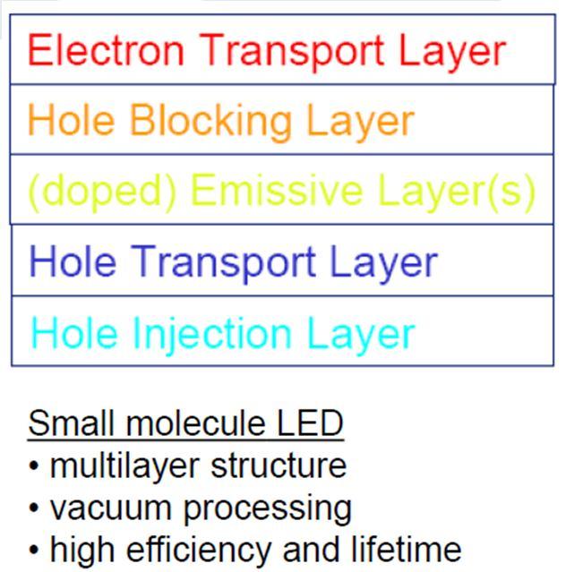
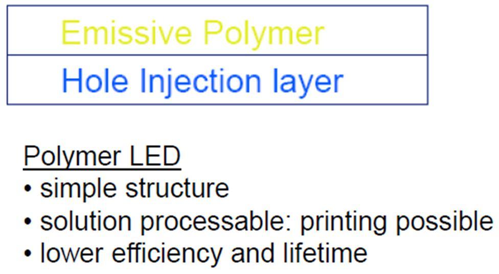
8 OLEDs technology: several approaches Two main materials: Small Molecule OLED (SMOLED) Polymer LED (PLED) Two main architecture: Bottom Emitting OLEDs Top Emitting OLEDs Small Molecule materials Use of small molecules High purity of materials Smooth surfaces Bottom emitting Light V Reflecting Electrode Light Emitting Material Transparent Electrode Transparent Substrate Light Light Emitting Polymers (LEP) Use of light-emitting polymers Hosts with different dopants, dyes and nanoparticles in order to obtain several colors V Transparent Electrode Light Emitting Material Reflecting Electrode Substrate Top emitting 8

9 Fabrication Technologies Small molecules Polymers OLED basic 9

10 OLED: addressing two markets Source: Novaled

")
 Sony XEL-1, 11\" TV set")
")
 Epson 40\" TV set,")
 OLEDs are an important")

 (2015) PANASONIC TX-65CZ950,")
11 OLEDs DISPLAYS! From early samples to marketed products Kodak LS633 photocamera, 2.2" AMOLED display (2003) Samsung S6 Edge, 5.1" (2015) Sony XEL-1, 11" TV set (2007) LG 55EC9300, 55" curved Full HD TV set, US$ 1999 (2014) LG G Flex LS995, 6.0" (2013) Epson 40" TV set, ink-jet printed, polymer-based (2004) OLEDs are an important success of the Organic Electronics LG 77EG9900, 77" flexible 4K TV set, US$ 50,000 (!?) (2015) PANASONIC TX-65CZ950, 65" curved 4K TV set (2015) (LG panel) Images:


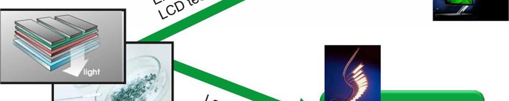
12 OLEDs for lighting OLEDs It is a Solid State Lighting technology, with LEDs and EL sources It is an answer for high efficiency very small or zero environmental impact It is THE answer for natural, large area, glare-free light tuneable colour flexible, thin and lightweight sources transparent sources dimmable sources


 General")


 Novaled")
13 OLEDs for lighting OLED lighting development is moving fast too! Several prototypes LG Chem (2009) General Electric chandelier World s first OLED lamp by OSRAM and Ingo Maurer design (2008) (price: ) Novaled transparent OLEDs (2010) Novaled Philips


 = 375 US$ PHILIPS Lumiblade various")
 luminance = 1.000 cd/m 2 life = 10.")
14 OLEDs for lighting OLED lighting development is moving fast too! first commercial devices in 2009 OSRAM Orbeos diameter = 80 mm efficacy = 25 lm/w CRI (Colour Rendering Index) = 80 price (at launch) = 375 US$ PHILIPS Lumiblade various dimensions and forms efficacy = 20 lm/w (white & RGB) luminance = cd/m 2 life = hours price (at launch) = 44 x 47 mm 2


")

 LG")


15 OLEDs for lighting OLED lighting development is moving fast too! to present (and coming) products OSRAM Novaled OSRAM Blackbody (FIAMM) LG Chem Konica Minolta Fraunhofer COMEDD AUDI etc. AUDI Novaled Konica Minolta Blackbody (FIAMM) LG Chem Fraunhofer COMEDD
16 OSRAM efficacy = 40 lm/w luminance = 2000 cd/m^2 CRI = 80 lifetime L70 = h working voltage = 6 V active area = up to > 11 cm^2 cost = N.A. OLEDs for lighting Characteristics of some OLED lighting products Announced best performances of OLED devices NEC Lighting & Yamagata Univ. efficacy = 156 lm/w luminance = 1000 cd/m^2 active area = 4 mm^2 LG Chem efficacy = 50+ lm/w luminance = cd/m^2 CRI = 90+ lifetime L70 = h working voltage = 6 or 8.5 V active area = up to 1000 cm^2 cost = $566/klm (680 US$/panel) OLED lighting average cost 200 US$/klm 20X LEDs IDTechEx (2014): market < $ $ Konica Minolta efficacy = 64 lm/w luminance = 1000 cd/m^2 lifetime L50 = h active area = 68 cm^2 cost = N.A. Konica Minolta efficacy = 139 lm/w luminance = 1000 cd/m^2 CRI = 81 lifetime L50 = h active area = 15 cm^2 source: Cintelliq (2014): OLEDs become a strong competitor to LEDs by 2016 By 2020: OLED panels priced at cd/m^2, and less than 14/klm By 2023: OLED panel production > 500 million of 100mm x 100mm panel equivalents
17 OLEDs for lighting Anyway, there are still "red brick walls" to face Lifetime Encapsulation New Barriers for large area and flexible devices integrated in-line production Devices Efficiency Light Outcoupling/Extraction intelligent glass substrates and lenses (micro lenses, pyramid array, prism foil) index-matched materials and adhesives encapsulation, for matched index plastic substrates Standardization Manufacturing Costs Improved Processes Lower Prices and High Production Volumes high throughput and material utilization efficiency for vacuum deposition solution processing and printing tooling promises must turn into reality for lower cost manufacturing, but must deliver high performance devices this red brick wall is becoming the most dominant one Investments, to move from R&D and pilot lines to real production source: OE-A - White Paper - Roadmap for Organic and Printed Electronics, 6th Ed. (June 2015)


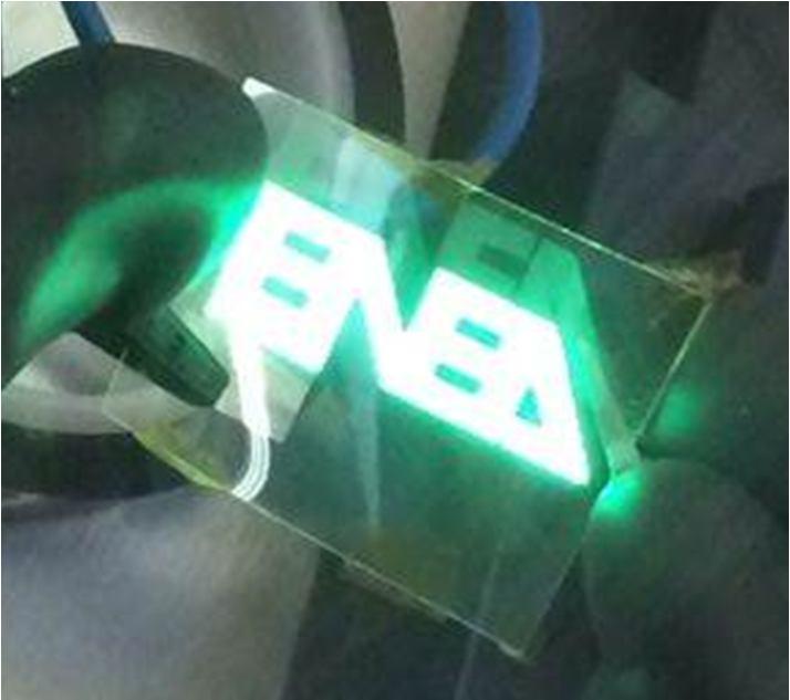
18 Lab. ENEA NANO competence OLEDs OPV OTFTs Innovative process technologies Raw materials recovery from waste Laboratory NANO is organized as a lab-scale full processing line for simulation, design, fabrication and test of materials, devices and systems of ORGANIC and PRINTED ELECTRONICS, its applications in horticulture, and study the recovery and recycling of raw materials from waste Activities address the EIT priorities for RAW MATERIALS Images: ENEA SSPT-PROMAS-NANO; COATEMA
19 thin film deposition of organic and inorganic materials through high vacuum techniques and from solution (thermal evaporation, sputtering, CVD, ALD, spin-coating, inkjet printing, roll to roll printing)) development of : innovative phosphorescent materials Innovative hybrid conductive transparent materials barrier layer by ALD structural, morphological, optical and electrical material characterizations evaluation of energy levels of materials design of device architectures, circuit and system layouts simulation of materials and devices OLEDs fabrication, encapsulation and electro-optical characterizations OLEDs lifetime optimization ENEA OLED expertise

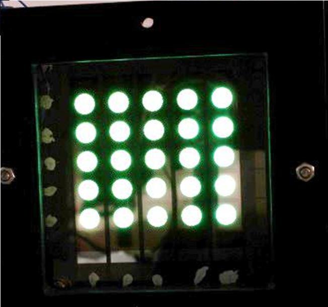
20 Lab. ENEA NANO competence OLEDs on glass

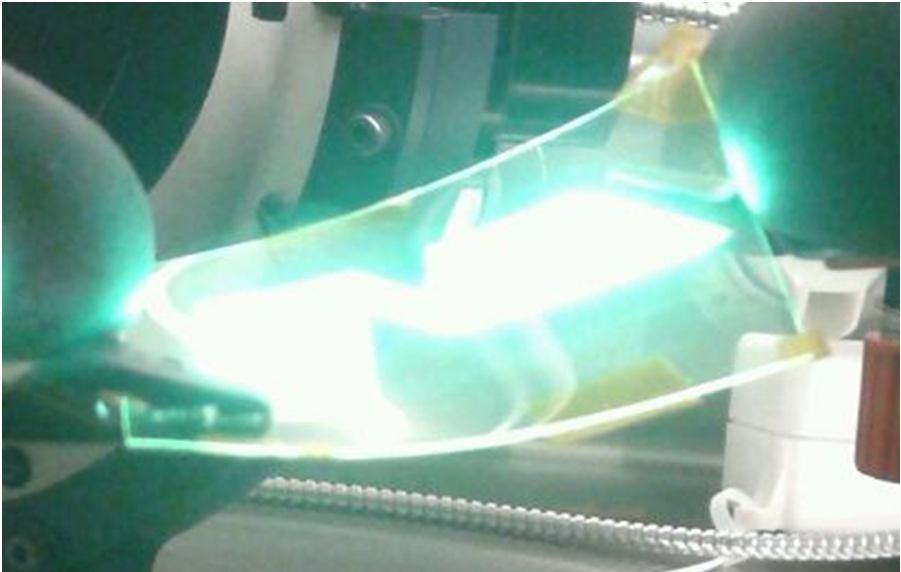
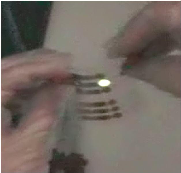
21 Lab. ENEA NANO competence OLEDs on plastic
22 Lab. ENEA NANO competence ENEA NANO - OLEDs activity Objectives Improvement of Performances of the devices, through materials devices architecture fabrication technologies (high through-put methods, printing techniques, etc.) simulations (physical and electrical) Stability and lifetime, and methods to improve them Life cycle of devices and systems to study low eco-impact materials and processes, to reduce the waste and improve the recovery of valuable materials Usefulness of the devices to develop and transfer useful knowledge to the companies and the public

23 Lab. ENEA NANO competence ENEA NANO OLEDs Materials and architecture Encapsulation Cathode EIL ETL HBL EML HTL HIL Anode Substrate Substrate Glass; PET; PEN; etc. Anode ITO; doped PEDOT:PSS; ZnO; AZO; etc. HIL - Hole Injection Layer PEDOT:PSS, Metal Oxides (MoO 3 ), CuPc HTL - Hole Transport Layer α-npd, TPD EML - Emitting Layer Small Molecules, Polymers, Blends and Nanocomposites deposited by evaporation in vacuum and from solution host materials: CBP, SimCP guest materials: Ir(Fppy)3, Ir(ppy)3, etc. HBL - Hole Blocking Layer BCP ETL - Electron Transport Layer Alq3 Cathode LiF + Al; Ca + Al; Li + Al; etc. Encapsulation rigid: glass lid + epoxy resin sealant + getter flexible: thin film encapsulation: inorganic barriers, organic-inorganic multilayer
24 Lab. ENEA NANO competence Improvement of the devices performances Anode surface treatments Charge injection layers (HIL, EIL) PEDOT:PSS, CuPc, LiF, etc. Low work-function cathodes Phosphorescent emitting materials Light outcoupling Materials: CBP + Ir(ppy)3; LiF/Al Turn-on voltage 2.0 V Luminance V Current efficiency 20 cd/a Efficacy 15 lm/w No light outcoupling


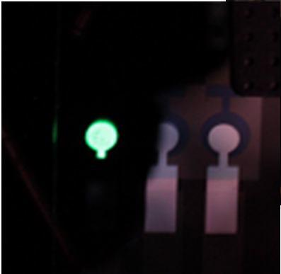
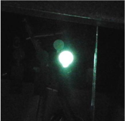
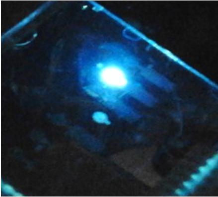
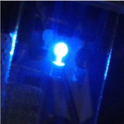
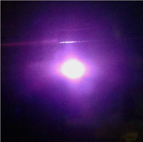
25 Lab. ENEA NANO competence White OLEDs Blue OLEDs Violet OLEDs Very wide spectrum 437 nm 672 nm DEV A EL Spectrum (a.u.) 0,70 0,65 0,60 0,55 0,50 0,45 0,40 0,35 0,30 0,25 0,20 0,15 0,10 0,05 0,00 no interlayer - red 3% 10nm - green 6% 10nm -0, W avelength (nm) 1mA 2,5mA 5mA 10mA 15mA Confidential - Unpublished results


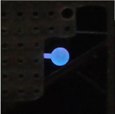
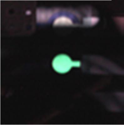
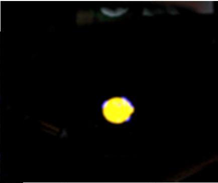
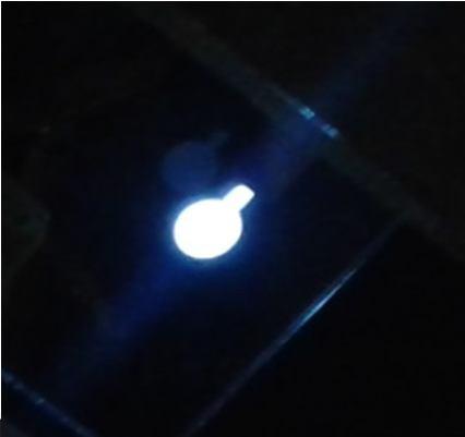
26 ENEA OLEDs Dimensions: few mm 2 up to some square cm Threshold voltage: 3.0 V Luminance: up to several thousands of cd/m 2 Luminance: cd/m 9 V White OLED for Lighting applications warm natural white cold white Encapsulated Organic Electronic Device With Improved Resistance To Degradation, P. Tassini, M. G. Maglione, E. Romanelli, P. Vacca, C. Minarini, United States Patent Application (2009)


27 ENEA OLEDs in white goods OLED prototypes to light the interior of refrigerator. Developed for Electrolux in the frame of the ALADIN Project, in collaboration with CRP, SAES, FERRANIA, CRF, CNR. Some wavelengths of light are able to maintain the freshness and nutritional properties of vegetables. 27

 we use ENEA violet OLED obtained with a")

 -0,05 300 400 500 600 700 800")
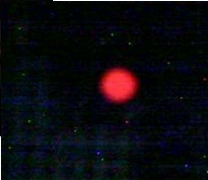
28 Innovation: OLED light in horticulture to enhance the growth of some vegetables An efficient lamp for plant growth must convert as much electrical energy as possible into Photosynthetically Active Radiation region energy (PAR nm) we use ENEA violet OLED obtained with a combination of blue and red wavelenghts Luminance (9V) 5000 Cd/cm 2 EL Spectrum (a.u.) 0,50 0,45 0,40 0,35 0,30 0,25 0,20 0,15 0,10 0,05 0,00 Glass/ITO/PEDOT:PSS/NDP/EML/BCP/Alq 3 /Ca(Al) -0, Wavelength (nm) Drogaggio EML 2% Drogaggio EML 4% Wavelength emission(nm) Peak Peak Peak 3 673

29 ENEA innovative materials for OLED in collaboration with Dept. of Chemistry, University of Naples Natural Pigments Inspire the Design of Biocompatible Materials in Organic Electronics: Melanins The use of such biodegradable materials can be an answer to the problem of electronic waste. For this reason growing attention is paid to the design and development of nature-inspired materials for organic electronics applications. Our idea is to use natural pigments (melanins) in OLED applications. Our main goals of the melanin-inspired research are: 1) the design, synthesis and characterization of new melanin-inspired photoluminescent materials for OLED applications; 2) the development of melanin-based material for ITO replacement. Melanin precursors HO HO HO N H NH 2 Chemical and physical properties Extremely low radiative quantum yield Photo- and electrical conductivity Broad band absorption in the entire UV-Vis spectrum Free radical and redox behavior HO Main goals of the melanin-inspired research line Design, synthesis and characterization of new melanin-inspired photoluminescent materials for OLED applications. Development of a melanin-based material for ITO replacement. Photovoltaic devices Melanins Photoactive and photoprotective materials Optoelectronic and energy storage devices Fields of application Sensors


30 OLED encapsulation results Not Encapsulated Devices Encapsulated Devices Not-Encapsulated Encapsulated SEM image optical image Visible Aging: A combination of Electrical and Time effect Very little effect on Encapsulated devices Encapsulation reduces electroluminescence decay and voltage shift Encapsulation problems Side penetration of oxygen and water-vapour through organic layers and metal-encapsulation interface O 2 Water vapour O 2 Water vapour Encapsulation Al Organic layers ITO Substrate Encapsulation Al Organic layers ITO Substrate 30
 has been obtained.")

).")
).")
31 Lab. ENEA NANO competence getter Encapsulation and lifetime studies Rigid encapsulation getter Water vapour transmission rate (WVTR) of 10-5 g/m 2 /day at room temperature (T = 25 C, RH = 50%; measured by ENEA electrical Ca test) has been obtained. US Patent 2009/ A1: "Encapsulated organic electronic device with improved resistance to degradation", 12/03/2009 Italian patent TO2007U000116: "Dispositivo elettronico organico incapsulato, con migliorata resistenza al degrado", 11/09/2007 In progress Study of the intrinsic degradation phenomena through shelf life experiments, performed at different storage conditions (by using a climate chamber). Flexible encapsulation Multilayer barrier of sputtered Al 2 O 3, on the device (Thin Film Encapsulation (TFE)). WVTR of 10-3 g/m 2 /day at room conditions (T = 25 C, RH = 50%; below the detection limit of our permeabilimeter (< 10-2 g/m 2 /day)) can be reached. Lamination of transparent barrier film (Foil Encapsulation (FE)). WVTR of 10-1 to 10-3 g/m 2 /day at room conditions (T = 25 C, RH = 50%; measured by permeabilimeter) has been achieved.


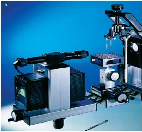
32 Lab. ENEA NANO competence OLEDs fabrication facilities KURT J. LESKER integrated process system: Evaporator, Sputter, Spin-coaters, integrated in a glove box with inert atmosphere OXFORD OpAL Atomic Layer Deposition system (ALD), for barrier layers deposition: Al2O3, SiN, SiO2 Modular and upgradable COATEMA Smartcoater roll-to-roll printing system: gravure and screen-printing, slot-die coating, lamination, inert atmosphere

, for")


 (EVG620")

33 Lab. ENEA NANO competence OLEDs fabrication facilities Clean room (class 100), for photolithography and chemical processes Excimer laser processing: Laser assisted deposition Crystallization PECVD cluster system Mask Aligner with Nano Imprint Lithography (NIL) (EVG620 NT) Direct Writing Laser system, for high resolution photolithography Ink-jet printing system Hot embossing system


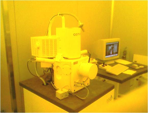

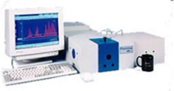
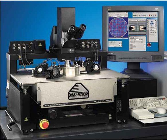
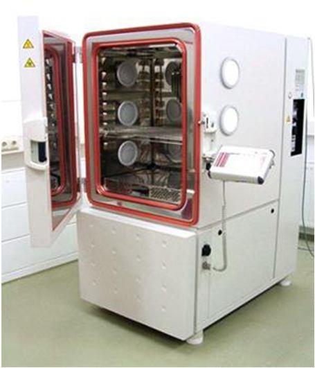
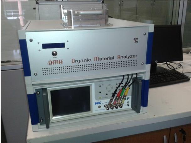
34 Lab. ENEA NANO competence OLEDs fabrication facilities SEM Electro-optical bench Probe station Organic Material Analyzer Profilometer Spectrofluorometer Climatic chamber Contact angle
 Maria Grazia Maglione C. R. ENEA Portici P.le E. Fermi, 1 80055 Portici (NA), Italy mariagrazia.maglione@enea.")
35 Department for Sustainability of the productive and territorial systems (SSPT) Division for Technologies and processes of the materials for the sustainability (SSPT-PROMAS) Laboratory for Nanomaterials and Devices (SSPT-PROMAS-NANO) Maria Grazia Maglione C. R. ENEA Portici P.le E. Fermi, Portici (NA), Italy mariagrazia.maglione@enea.it ENEA Portici Research Centre Laboratory for Nanomaterials and Devices (SSPT-PROMAS-NANO) Head of lab.: Carla Minarini carla.minarini@enea.it
OLEDs for lighting State of the art and ENEA competence
 NanoItaly 2015 Roma - Italy Department for Sustainability of the productive and territorial systems (SSPT) Division for Technologies and processes of the materials for the sustainability (SSPT-PROMAS)
An Overview of OLED Display Technology
 page:1 An Overview of OLED Display Technology Homer Antoniadis OSRAM Opto Semiconductors Inc. San Jose, CA page:2 Outline! OLED device structure and operation! OLED materials (polymers and small molecules)!
[1.9] AMOLED 공정 Introduction OLED Materials Patterning Process Process Equipments
![[1.9] AMOLED 공정 Introduction OLED Materials Patterning Process Process Equipments](/thumbs/73/69073032.jpg "[1.9] AMOLED 공정 Introduction OLED Materials Patterning Process Process Equipments") [1.9] AMOLED 공정 1.9.1. Introduction 1.9.2. OLED Materials 1.9.3. Patterning Process 1.9.4. Process Equipments OLED : Organic Light Emitting Diode Organic EL : Organic Electroluminescent 재료및공정 재료의발광메카니즘
[1.9] AMOLED 공정 1.9.1. Introduction 1.9.2. OLED Materials 1.9.3. Patterning Process 1.9.4. Process Equipments OLED : Organic Light Emitting Diode Organic EL : Organic Electroluminescent 재료및공정 재료의발광메카니즘
Development of OLED Lighting Applications Using Phosphorescent Emission System
 Development of OLED Lighting Applications Using Phosphorescent Emission System Kazuhiro Oikawa R&D Department OLED Lighting Business Center KONICA MINOLTA ADVANCED LAYERS, INC. October 10, 2012 Outline
The Company. A leading OLED player
 The Company A leading OLED player Novaled is the company to trade with, work for and invest in. Our company focuses on proprietary organic materials and complementary innovative technologies for superior
Phosphorescent OLED Technologies: The Next Wave. Plastic Electronics Conference Oct 9, 2012
 Phosphorescent OLED Technologies: The Next Wave Plastic Electronics Conference Oct 9, 2012 UDC Company Focus IP innovator, technology developer, patent licensor and materials supplier for the rapidly growing
Solution Processable OLEDs. Anna Hayer EuroDisplay /09/2013
 Solution Processable LEDs Merck KGaA Anna Hayer EuroDisplay 2013 Content 1 Introduction 2 LED Basics 3 Challenges for Solution Processing 4 Current Results 5 Summary 2 EuroDisplay 2013 Hayer - Merck Solution
OLED Technology Introduction
 OLED Technology Introduction An organic light emitting diode (OLED) consists of several semiconducting organic layers sandwiched between two electrodes at least one of them being transparent. A simplified
High Efficiency White OLEDs for Lighting
 CIE-y Journal of Photopolymer Science and Technology Volume 25, Number 3 (2012) 321 326 2012CPST High Efficiency White OLEDs for Lighting Takuya Komoda, Kazuyuki Yamae, Varutt Kittichungchit, Hiroya Tsuji
ORGANIC LIGHT EMITTING DIODES (OLEDS): TECHNOLOGIES AND GLOBAL MARKETS
: TECHNOLOGIES AND GLOBAL MARKETS") ORGANIC LIGHT EMITTING DIODES (OLEDS): TECHNOLOGIES AND GLOBAL MARKETS SMC069D September 2015 Gupta A. S. Project Analyst ISBN: 1-62296-133-1 BCC Research 49 Walnut Park, Building 2 Wellesley, MA 02481
ORGANIC LIGHT EMITTING DIODES (OLEDS): TECHNOLOGIES AND GLOBAL MARKETS SMC069D September 2015 Gupta A. S. Project Analyst ISBN: 1-62296-133-1 BCC Research 49 Walnut Park, Building 2 Wellesley, MA 02481
PROCESS TECHNOLOGIES FOR ADVANCED ORGANIC ELECTRONIC DEVICES: MICRODISPLAYS, LIGHTING AND SOLAR CELLS
 PROCESS TECHNOLOGIES FOR ADVANCED ORGANIC ELECTRONIC DEVICES: MICRODISPLAYS, LIGHTING AND SOLAR CELLS Dr. Christian May Fraunhofer IPMS - Center for Organic Materials and Electronic Devices Dresden COMEDD
Development of OLED Lighting Panel with World-class Practical Performance
 72 Development of OLED Lighting Panel with World-class Practical Performance TAKAMURA MAKOTO *1 TANAKA JUNICHI *2 MORIMOTO MITSURU *2 MORI KOICHI *3 HORI KEIICHI *4 MUSHA MASANORI *5 Using its proprietary
ADDING AN O TO LEDS STATUS AND PERSPECTIVES OF ORGANIC LIGHT EMITTING DIODES PAWEL E. MALINOWSKI, TUNGHUEI KE LED EVENT 2017
 ADDING AN O TO LEDS STATUS AND PERSPECTIVES OF ORGANIC LIGHT EMITTING DIODES PAWEL E. MALINOWSKI, TUNGHUEI KE LIVING ROOM NOT SO LONG AGO... 2 Source: Warner Bros. Incadescent CRT 3 Source: Warner Bros.
Silole Derivative Properties in Organic Light Emitting Diodes
 Silole Derivative Properties in Organic Light Emitting Diodes E. Duncan MLK HS Physics Teacher Mentors: Prof. Bernard Kippelen & Dr. Benoit Domercq Introduction Theory Methodology Results Conclusion Acknowledgements
:: Reduce needs for heat dissipation components. :: Extend battery life in mobile products. :: Save power and reduce heat generation in TVs
 UniversalPHOLED Technology and Materials UniversalPHOLED Phosphorescent OLED technology and materials offer record-breaking performance to bring competitive advantages to your OLED display and lighting
P I SCALE Creating an Open Access Flexible O L E D P ilo t L in e S e r vic e
 P I SCALE Creating an Open Access Flexible O L E D P ilo t L in e S e r vic e Pavel Kudlacek pavel.kudlacek@tno.nl P I - SCALE for 2017Flex 1 Lighting c h a lle n g e L ig h t in g c h a lle n g e At least
UniMCO 4.0: A Unique CAD Tool for LED, OLED, RCLED, VCSEL, & Optical Coatings
 UniMCO 4.0: A Unique CAD Tool for LED, OLED, RCLED, VCSEL, & Optical Coatings 1 Outline Physics of LED & OLED Microcavity LED (RCLED) and OLED (MCOLED) UniMCO 4.0: Unique CAD tool for LED-Based Devices
High Performance White OLEDs Technologies for Lighting
 High Performance White OLEDs Technologies for Lighting 10 October, 2012 Takuya Komoda Core Technologies Development Center Panasonic Corporation Contents 2 1. Expectation to the Next Generation Lighting
ADVANCEMENTS IN GRAVURE TECHNOLOGY: FOR SUSTAINABILITY AND GROWTH PRINTED LIGHTING TECHNOLOGY
 ADVANCEMENTS IN GRAVURE TECHNOLOGY: FOR SUSTAINABILITY AND GROWTH PRINTED LIGHTING TECHNOLOGY Marc Chason Marc Chason and Associates, Inc. marcchason@sbcglobal.net January 17, 2012 Logic Driven Value Chain
Thin-Film Encapsulation of Organic Light Emitting Devices (OLEDs) Dr. Emilie Galand Huntsman Advanced Materials CSEM Plastic Optoelectronics - Basel
 Dr. Emilie Galand Huntsman Advanced Materials CSEM Plastic Optoelectronics - Basel") Thin-Film Encapsulation of Organic Light Emitting Devices (OLEDs) Dr. Emilie Galand CSEM Plastic Optoelectronics - Basel 25th June 2010 About Huntsman Huntsman is a global manufacturer and marketer of
Thin-Film Encapsulation of Organic Light Emitting Devices (OLEDs) Dr. Emilie Galand CSEM Plastic Optoelectronics - Basel 25th June 2010 About Huntsman Huntsman is a global manufacturer and marketer of
Stacked OLEDs for Lighting Applications - Improvement of the yellow building block
 Stacked OLEDs for Lighting Applications Improvement of the yellow building block 13/12/2010 Carola Diez Osram Opto Semiconductors GmbH and University of Augsburg OLED Lighting White organic light emitting
Organic light emitting diodes for display technology
 Organic light emitting diodes for display technology Shamna Shamsudeen MScTI - ZITI-Heidelberg University OLED ZITI, Uni Heidelberg Page1 What s Light Light: Visible part of EM spectra. Ref:[1] Thermoluminescence:
OLED for Lighting. Outline
 OLED for Lighting Monica Katiyar MME & SCDT Indian Institute of Technology, Kanpur Outline Lighting Photometry and colorimetry Some examples Various approaches to W-OLED 1 500,000 years ago Lighting Gas
 Page 1 of 8 Main > Electronics > Computers How OLEDs Work by Craig Freudenrich, Ph.D. Introduction to How OLEDs Work Imagine having a high-definition TV that is 80 inches wide and less than a quarter-inch
Fundamentals of Organic Light Emitting Diode
 Fundamentals of Organic Light Emitting Diode M. F. Rahman* 1 and M. Moniruzzaman 2 Organic light emitting diode (OLED) has drawn tremendous attention in optoelectronic industry over the last few years.
Performance Comparison of Bilayer and Multilayer OLED
 Performance Comparison of Bilayer and Multilayer OLED Akanksha Uniyal, Poornima Mittal * Department of Electronics and Communication School of Engineering and Technology Graphic Era University, Dehradun-248002,
Process Dependent Performance of Slot Die Coated OLED-Multilayers (TALK)
") Process Dependent Performance of Slot Die Coated OLED-Multilayers (TALK) Sebastian Raupp 1,2, Lisa Merklein 1,2, Philip Scharfer 1,2 and Wilhelm Schabel 1 1 Institute of Thermal Process Engineering, Thin
Process Dependent Performance of Slot Die Coated OLED-Multilayers (TALK) Sebastian Raupp 1,2, Lisa Merklein 1,2, Philip Scharfer 1,2 and Wilhelm Schabel 1 1 Institute of Thermal Process Engineering, Thin
Development and Mass-Production of an OLED Lighting Panel - Most-Promising Next-Generation Lighting -
 Development and Mass-Production of an OLED Lighting Panel - Most-Promising Next-Generation Lighting - 47 KEIICHI HORI *1 JOJI SUZUKI *2 MAKOTO TAKAMURA *3 JUNICHI TANAKA *4 TSUTOMU YOSHIDA *5 YOSHITAKA
OLED Status quo and our position
 OLED Status quo and our position Information Day 2013 A Deep Dive into the LC&OLED Business Dr. Udo Heider Vice President OLED Darmstadt, Germany June 26, 2013 Disclaimer Remarks All comparative figures
 Chapter 1 Introduction --------------------------------------------------------------------------------------------------------------- 1.1 Overview of the Organic Light Emitting Diode (OLED) Displays Flat
High Value Applications and High Growth Markets for Printed Electronics
 High Value Applications and High Growth Markets for Printed Electronics Marc Chason Marc Chason and Associates, Inc. marcchason@sbcglobal.net October 5, 2011 Why SSL for Printed Electronics? Four Themes
OLED COMPANY. for Display & Lighting Applications
 OLED COMPANY for Display & Lighting Applications Novaled: World-class OLED Player Novaled creates value for OLED (Organic Light Emitting Diode) and Organic Electronics (OE) makers. Novaled s PIN technology
Content. Core Technology (Short introduction) LCMO (Light Controlled Molecular Orientation) technology
 LCMO (Light Controlled Molecular Orientation) technology") Content Core Technology (Short introduction) LCMO (Light Controlled Molecular Orientation) technology LCMO Patterned Films for Light management : Applications Examples LCMO- Photo Patterned Retarders LCMO-
Content Core Technology (Short introduction) LCMO (Light Controlled Molecular Orientation) technology LCMO Patterned Films for Light management : Applications Examples LCMO- Photo Patterned Retarders LCMO-
Organic Light-Emittin g Devices
 Joseph Shinar Organic Light-Emittin g Devices A Survey Preface Contributors v xv 1 Introduction to Organic Light-Emitting Device s Joseph Shinar and Vadim Savvateev 1 1.1 Introduction 1 1.2 Basic Electronic
High Power Efficiencies at Record Lifetimes: NOVALED s PIN-OLEDs
 High Power Efficiencies at Record Lifetimes: NOVALED s PIN-OLEDs Harald Gross, Jan Blochwitz-Nimoth, Jan Birnstock, Ansgar Werner, Michael Hofmann, Philipp Wellmann, Tilmann Romainczyk, Sven Murano, Andrea
Gary Mandle Sr. Product Manager Professional Display Products
 Gary Mandle Sr. Product Manager Professional Display Products rganic Light Emitting Diode It is: An emissive output o backlight o plasma gasses Self luminous matrix array Created by sandwiching several
IGM. Development of Vapor Deposition Processes for OLEDs. Bachelor Thesis. Prof. Dr.-Ing. N. Frühauf. 28th of September Alexandru Andrei Lungu
 IGM Institut für Großflächige Mikroelektronik Institut für Großflächige Mikroelektronik Prof. Dr.-Ing. N. Frühauf Development of Vapor Deposition Processes for OLEDs Bachelor Thesis 28th of September 2014
Advancement in the Technology of Organic Light Emitting Diodes
 IOSR Journal of Electrical and Electronics Engineering (IOSR-JEEE) e-issn: 2278-1676,p-ISSN: 2320-3331, PP 06-10 www.iosrjournals.org Advancement in the Technology of Organic Light Emitting Diodes Rohan
ORGANIC ELECTRONICS PROCESS DEVELOPMENT AND ENCAPSULATION TECHNOLOGIES
 FRAUNHOFER INSTITUTE FOR ORGANIC ELECTRONICS, ELECTRON BEAM AND PLASMA TECHNOLOGY FEP ORGANIC ELECTRONICS PROCESS DEVELOPMENT AND ENCAPSULATION TECHNOLOGIES 2 PROFILE Fraunhofer FEP combines research and
1. Publishable summary
 1. Publishable summary 1.1. Project objectives. The target of the project is to develop a highly reliable high brightness conformable low cost scalable display for demanding applications such as their
LG Display OLED Light. 1. Corporate Overview 2. Market Trend 3. New Product 4. Advantages of OLED light 5. Applicable Areas 6.
 OLED Light 1 LG Display OLED Light 1. Corporate Overview 2. Market Trend 3. New Product 4. Advantages of OLED light 5. Applicable Areas 6. Price Indication 1. Corporate Overview LG Display offers a variety
VARIOUS DISPLAY TECHNOLOGIESS
 VARIOUS DISPLAY TECHNOLOGIESS Mr. Virat C. Gandhi 1 1 Computer Department, C. U. Shah Technical Institute of Diploma Studies Abstract A lot has been invented from the past till now in regards with the
Present status of Roll-to-Roll Fabrication for OLED lighting
 Present status of Roll-to-Roll Fabrication for OLED lighting Michael Stanel, Tomasz Wański, Stefan Mogck Fraunhofer Institute for Organic Electronics, Electron Beam and Plasma Technology FEP AIMCAL, Web
Printed Solid State Lighting Update
 Printed Solid State Lighting Update Marc Chason Marc Chason and Associates, Inc. marcchason@sbcglobal.net May 7, 2013 Two Themes Overview of the 2013 inemi Solid State Illumination (SSI ) Roadmap chapter
Advanced Display Technology (continued) Lecture 13 October 4, 2016 Imaging in the Electronic Age Donald P. Greenberg
 Lecture 13 October 4, 2016 Imaging in the Electronic Age Donald P. Greenberg") Advanced Display Technology (continued) Lecture 13 October 4, 2016 Imaging in the Electronic Age Donald P. Greenberg Cost of HDTV Displays Price $ Plasma Projection TV s LCD s Diagonal Inches Cost of HDTV
Advanced Display Technology (continued) Lecture 13 October 4, 2016 Imaging in the Electronic Age Donald P. Greenberg Cost of HDTV Displays Price $ Plasma Projection TV s LCD s Diagonal Inches Cost of HDTV
Development of Extremely High Efficacy White OLED with over 100 lm/w
 Journal of Photopolymer Science and Technology Volume 27, Number 3 (2014) 357 361 2014SPST Development of Extremely High Efficacy White OLED with over 100 lm/w Nobuhiro Ide, Kazuyuki Yamae, Varutt Kittichungchit,
OLED Lighting in Automotive Applications State of the Art and Future Demands. OLEDs World Summit 2017, San Francisco, Dr. Werner Thomas, AUDI AG
 OLED Lighting in Automotive Applications State of the Art and Future Demands OLEDs World Summit 2017, San Francisco, Dr. Werner Thomas, AUDI AG 2 Agenda 1. Overview 1 st automotive series applications
JOURNAL OF DISPLAY TECHNOLOGY, VOL. 5, NO. 12, DECEMBER
 JOURNAL OF DISPLAY TECHNOLOGY, VOL. 5, NO. 12, DECEMBER 2009 541 Dual-Plate OLED Display (DOD) Embedded With White OLED Chang-Wook Han, Hwa Kyung Kim, Hee Suk Pang, Sung-Hoon Pieh, Chang Je Sung, Hong
Organic Electronic Devices
 Organic Electronic Devices Week 5: Organic Light-Emitting Devices and Emerging Technologies Lecture 5.1: Introduction to Organic Light-Emitting Devices Bryan W. Boudouris Chemical Engineering Purdue University
IOSR Journal of Engineering (IOSRJEN) ISSN (e): , ISSN (p): Volume 2, PP Organic Led. Figure 1.
 ISSN (e): , ISSN (p): Volume 2, PP Organic Led. Figure 1.") IOSR Journal of Engineering (IOSRJEN) ISSN (e): 2250-3021, ISSN (p): 2278-8719 Volume 2, PP 46-51 www.iosrjen.org Organic Led Prof.Manoj Mishra 1, Sweety Vade 2,Shrutika Sawant 3, Shriwari Shedge 4, Ketaki
IOSR Journal of Engineering (IOSRJEN) ISSN (e): 2250-3021, ISSN (p): 2278-8719 Volume 2, PP 46-51 www.iosrjen.org Organic Led Prof.Manoj Mishra 1, Sweety Vade 2,Shrutika Sawant 3, Shriwari Shedge 4, Ketaki
Sep 09, APPLICATION NOTE 1193 Electronic Displays Comparison
 Sep 09, 2002 APPLICATION NOTE 1193 Electronic s Comparison Abstract: This note compares advantages and disadvantages of Cathode Ray Tubes, Electro-Luminescent, Flip- Dot, Incandescent Light Bulbs, Liquid
Joint Development of Ultra-Bright, Inorganic EL Light-Emitting Materials. November 2, 2005 KURARAY CO., LTD.
 Joint Development of Ultra-Bright, Inorganic EL Light-Emitting Materials November 2, 2005 KURARAY CO., LTD. Sales Trends of Display-related Products (Kuraray (standalone)) FY1994 FY1999 FY2004 Sales Ratio
AMOLED Manufacturing Process Report SAMPLE
 AMOLED Manufacturing Process Report SAMPLE 2018 AMOLED Manufacturing Process Report The report analyzes the structure and manufacturing process by dividing AMOLED into small & medium-sized rigid OLED,
PROGRESS OF OLED TECHNOLOGY FOR LIGHTING
 PROGRESS OF OLED TECHNOLOGY FOR LIGHTING M. Anandan (SID) Organic Lighting Technologies LLC Austin Texas 1 OLED LAMPS 2 OLED: LIGHT GENERATION 3 OLED: FLUORESCENT 4 OLED: PHOSPHORESCENT 5 THREE FAMILIES
P-224: Damage-Free Cathode Coating Process for OLEDs
 P-224: Damage-Free Cathode Coating Process for OLEDs Shiva Prakash DuPont Displays, 6 Ward Drive, Santa Barbara, CA 937, USA Abstract OLED displays require the growth of inorganic films over organic films.
Organic Light Emitting Devices
 Organic Light Emitting Devices From Displays to Lighting By G. Parthasarathy, J. Liu, and A. R. Duggal Recently there has been significant interest in electroluminescence from organic materials. Driven
Advanced Display Manufacturing Technology
 Advanced Display Manufacturing Technology John Busch Vice President, New Business Development Display and Flexible Technology Group September 28, 2017 Safe Harbor This presentation contains forward-looking
Scalable self-aligned active matrix IGZO TFT backplane technology and its use in flexible semi-transparent image sensors. Albert van Breemen
 Scalable self-aligned active matrix IGZO TFT backplane technology and its use in flexible semi-transparent image sensors Albert van Breemen Image sensors today 1 Dominated by silicon based technology on
Zeon PDF Driver Trial
 OLED Technology and Product Development in RiTdisplay Chorng-Shyr Jou RiTdisplay csjou@ritdisplay.com 1 Contents I. The Technologies & Challenge of OLED II. The Application of OLED III.Who are Working
Present and future of OLED lighting
 Present and future of OLED lighting Dr. Wolfgang Dötter Authorized Company Officer OLEDWorks Global Q-EHS Manager & Senior Integral Project Manager 1 Vision In 10 years there will be only Solid State Lighting;
Quantum Dot Solutions for Lighting and Display Applications. Frank Ignazzitto APEC Conference February 9, 2012
 Quantum Dot Solutions for Lighting and Display Applications Frank Ignazzitto APEC Conference February 9, 2012 QD Vision s Focused & Integrated Approach The only quantum dot company focused solely on displays
PUBLISHABLE Summary To provide OLED stacks with improved reliability Provide improved thin film encapsulation
 PUBLISHABLE Summary SCOOP is a European funded project (FP7 project number 287595 SCOOP). It is focused on OLED technology, microdisplays based on the combination of OLED with CMOS technology, and innovative
Hole-Confining Concept for Blue Organic Light Emitting Diode
 Hole-Confining Concept for Blue Organic Light Emitting Diode A thesis submitted to the Division of Research and Advanced Studies of the University of Cincinnati in partial fulfillment of the requirements
High Brightness LEDs. Light Sources on Steroids
 High Brightness LEDs Light Sources on Steroids Course: Photonics and Optical Communications Instructor: Prof. D. Knipp Spring 2007, 20 th April, 2007 Presenter: Borislav Hadzhiev Overview Principle of
OLED vs. LED Lighting
 OLED vs. LED Lighting OLED lighting is an energy efficient solid state lighting technology. It has however come to the market second after LED lighting. They have a similar value proposition but LED is
Flexible Electronics Production Deployment on FPD Standards: Plastic Displays & Integrated Circuits. Stanislav Loboda R&D engineer
 Flexible Electronics Production Deployment on FPD Standards: Plastic Displays & Integrated Circuits Stanislav Loboda R&D engineer The world-first small-volume contract manufacturing for plastic TFT-arrays
High contrast tandem organic light emitting devices employing transparent intermediate nano metal layers and a phase shifting layer
 Edith Cowan University Research Online ECU Publications 2012 2012 High contrast tandem organic light emitting devices employing transparent intermediate nano metal layers and a phase shifting layer Baofu
LG OLED Light Panel. Flexible panels
 LG OLED Light Panel Flexible panels Handling Instruction A. Handling and Safety 1. Unpack packing box with care. Remove packing trays gently and carefully from packing box. 2. During unloading and handling,
Introduction to OLED lighting and key challenges for the industry
 Introduction to OLED lighting and key challenges for the industry Dr. Wolfgang Doetter Authorized Company Officer OLEDWorks Global Q-EHS Manager & Senior Integral Project Manager 1 OLEDs A new perception
PROJECT FINAL REPORT
 PROJECT FINAL REPORT Grant Agreement number: 215934 Project acronym: Project title: Funding Scheme: COMBOLED Combined Organic LED Technology for Large Area Transparent and low cost lighting Applications
Advances in Roll-to-Roll Imprint Lithography for Display Applications Using Self Aligned Imprint Lithography. John G Maltabes HP Labs
 Advances in Roll-to-Roll Imprint Lithography for Display Applications Using Self Aligned Imprint Lithography John G Maltabes HP Labs Outline Introduction Roll to Roll Challenges and Benefits HP Labs Roll
center for organic materials and electronic devices dresden
 F R A U N H O F E R I N S T I T U T e F o R P h o t o n i c M i c r o S y s t e m s I P M S center for organic materials and electronic devices dresden p r e f a c e Dr. Christian May Head of Business
New Worlds for Polymers: Organic Transistors, Light Emitting Diodes, and Optical Waveguides Ed Chandross
 New Worlds for Polymers: Organic Transistors, Light Emitting Diodes, and Optical Waveguides Ed Chandross Materials Chemistry, LLC 1 Polymers in the Electronic Industry Enabling Materials Active Materials?
OLED AND THIN-FILM ENCAPSULATION TECHNOLOGIES FOR MICRODISPLAYS
 OLED AND THIN-FILM ENCAPSULATION TECHNOLOGIES FOR MICRODISPLAYS Tony Maindron, PhD, CEA-Leti, France London, February, 21-22, 2017 OUTLINE Introduction OLED technology OLED for microdisplays Thin-film
Introduction... 4 About the author... 6 What is an OLED? OLED: An Organic Light Emitting Device... 7 Different kinds of OLEDs...
 Table of Contents Introduction... 4 About the author... 6 What is an OLED?... 7 OLED: An Organic Light Emitting Device... 7 Different kinds of OLEDs... 9 How an OLED display is made... 14 The backplane...
Organic Light Emitting Diodes (OLEDs) Physics 496/487 Matt Strassler
 Physics 496/487 Matt Strassler") Organic Light Emitting Diodes (OLEDs) Physics 496/487 Matt Strassler Why OLEDs Lighting efficiency Incandescent bulbs are inefficient Fluorescent bulbs give off ugly light LEDs (ordinary light emitting
Organic Light Emitting Diodes (OLEDs) Physics 496/487 Matt Strassler Why OLEDs Lighting efficiency Incandescent bulbs are inefficient Fluorescent bulbs give off ugly light LEDs (ordinary light emitting
Brief Review of OLED Technology
 Brief Review of OLED Technology Cheah Kok Wai ( 謝國偉 ) Department of Physics and Centre for Advanced Luminescence Materials ( 先進發光材料中心 ) Hong Kong Baptist University ( 香港浸會大學 ) Kowloon Tong ( 九龍塘 ), Hong
Organic Light Emitting Diodes
 ISSN: 2278 0211 (Online) Organic Light Emitting Diodes Badisa Sai Ram Krsihna Final Year B.Tech, Dept. of ECE, KL University, Vaddeswaram, AP, India Angadi Suresh Associate Professor B.Tech, Dept. of ECE,
OLED ON CMOS: WHAT ABOUT THINNING AND BENDING?
 Large cost-effective OLED microdisplays and their applications OLED ON CMOS: WHAT ABOUT THINNING AND BENDING? IDW2017 tony.maindron@cea.fr T. Maindron, B. Chambion, A. Vandeneynde, S. Gétin, M. Provost,
OLEDWorks OLED Panel Brite Amber Marker Light
 1 OLEDWorks OLED Panel Brite Amber Marker Light Thin and healthy OLED-light When it comes to lighting OLEDs inspire on a whole different level. There is the unique quality of the light itself. In combination
Simulation of Mixed-Host Emitting Layer based Organic Light Emitting Diodes
 Simulation of Mixed-Host Emitting Layer based Organic Light Emitting Diodes C. RIKU a,, Y. Y. KEE a, T. S. ONG a, S. S. YAP b and T. Y. TOU a* a Faculty of Engineering, Multimedia University, 631000 Cyberjaya,
Advanced Display Technology Lecture #12 October 7, 2014 Donald P. Greenberg
 Visual Imaging and the Electronic Age Advanced Display Technology Lecture #12 October 7, 2014 Donald P. Greenberg Pixel Qi Images Through Screen Doors Pixel Qi OLPC XO-4 Touch August 2013 http://wiki.laptop.org/go/xo-4_touch
Final Technical Progress Report
 Final Technical Progress Report Polymer OLED White Light Development Program (#DE-FC26-04NT41947) Submitted to: US Department of Energy (DOE) National Energy Technology Laboratory (NETL) Submitted by:
AIXTRON in EXCILIGHT project
 AIXTRON SE AIXTRON in EXCILIGHT project Gintautas Simkus ABOUT AIXTRON 2 Who we are Headquarter based in Herzogenrath, Germany Worldwide presence with 14 sales/representatives offices and production facilities
OLED Display & OLED Lighting: Technology Trends & Market Forecast. Jennifer Colegrove, Ph.D. VP, Emerging Display Technologies, NPD DisplaySearch
 OLED Display & OLED Lighting: Technology Trends & Market Forecast Jennifer Colegrove, Ph.D. VP, Emerging Display Technologies, NPD DisplaySearch 2 Outline OLED Display Technology and Market Forecast» New
Press Release Plastic Electronics 2013 October 8th 10th, 2013, in Dresden/Germany Hall 2, booth no. 292 (joint booth of Organic Electronic Saxony)
") Press Release Plastic Electronics 2013 October 8th 10th, 2013, in Dresden/Germany Hall 2, booth no. 292 (joint booth of Organic Electronic Saxony) Flexible OLED from the roll Tridonic Dresden and Fraunhofer
Press Release Plastic Electronics 2013 October 8th 10th, 2013, in Dresden/Germany Hall 2, booth no. 292 (joint booth of Organic Electronic Saxony) Flexible OLED from the roll Tridonic Dresden and Fraunhofer
OLED display technology
 American Journal of Optics and Photonics 2014; 2(3): 32-36 Published online June 30, 2014 (http://www.sciencepublishinggroup.com/j/ajop) doi: 10.11648/j.ajop.20140203.13 OLED display technology Askari
LIGHT EMITTING POLYMER from
 19 Electronics Electrical Instrumentation Seminar Topics Page 2 Introduction-Imagine these scenarios - After watching the breakfast news on TV, you roll up the set like a large handkerchief, and stuff
ACKNOWLEDGEMENT. An organic light-emitting diode (OLED), also light emitting
, also light emitting") An organic light-emitting diode (OLED), also light emitting polymer (LEP) and organic electro-luminescence (OEL), is any lightemitting diode (LED) whose emissive electroluminescent layer is composed of
An organic light-emitting diode (OLED), also light emitting polymer (LEP) and organic electro-luminescence (OEL), is any lightemitting diode (LED) whose emissive electroluminescent layer is composed of
Wide color gamut industry issues and market status
 Wide color gamut industry issues and market status Son, Seungkyu Richard November 3th, 2016 2 Wide color gamut display, essential for high-end displays With the appearance of products with wide color gamut
cintelliq Limited St. John s Innovation Centre Cowley Road Cambridge CB4 0WS :
 OLED Lighting: Moving from Market Entry to Volume Manufacturing Presented at The Plastic Electronics Conference, 2012, Dresden By Craig Cruickshank (CEO) 11 October 2012 cintelliq Limited St. John s Innovation
EFFICIENT PHOSPHORESCENT OLEDS BASED ON VACUUM DEPOSITION TECHNOLOGY. Desta Gebeyehu Department of Physics Addis Ababa University.
 EFFICIENT PHOSPHORESCENT OLEDS BASED ON VACUUM DEPOSITION TECHNOLOGY Desta Gebeyehu Department of Physics Addis Ababa University and K. Leo Institute of Applied Photophysics (IAPP) Technology University
Displays and framebuffers
 Reading Optional Displays and framebuffers Brian Curless CSE 557 Autumn 2017 OpenGL Programming Guide (the red book available online): First four sections of chapter 2 First section of chapter 6 Foley
High-resolution screens have become a mainstay on modern smartphones. Initial. Displays 3.1 LCD
 3 Displays Figure 3.1. The University of Texas at Austin s Stallion Tiled Display, made up of 75 Dell 3007WPF LCDs with a total resolution of 307 megapixels (38400 8000 pixels) High-resolution screens
Low-haze light extraction from organic light-emitting diode lighting with auxiliary electrode by selective microlens arrays
 4182 OPTICS LETTERS / Vol. 38, No. 20 / October 15, 2013 Low-haze light extraction from organic light-emitting diode lighting with auxiliary electrode by selective microlens arrays Ju Hyun Hwang, 1 Tae
Industrial Inline Control for Advanced Vacuum Roll to Roll Systems. Gerhard Steiniger Web inspection - surface Quallity control 7.
 Industrial Inline Control for Advanced Vacuum Roll to Roll Systems Gerhard Steiniger Web inspection - surface Quallity control 7.4-7684 1 Industrial Inline Control for Advanced Vacuum Roll to Roll Systems
Microcavity OLED using Ag electrodes
 Microcavity OLED using Ag electrodes Huajun Peng, Xiuling Zhu, Jiaxin Sun, Xiaoming Yu, Man Wong and Hoi-Sing Kwok Center for Display Research, Department of Electrical and Electronic Engineering Hong
Light, Bright, and. Julie Brown Universal Display Corporation.
 Light, Bright, and Julie Brown Universal Display Corporation jjbrown@universaldisplay.com May 3, 2006 A Perspective OLEDs Yesterday OLEDs Today OLEDs Tomorrow Milestones in OLEDs (1960-2000) 1963 Pope
ORGANIC DISPLAYS and Driving Circuits
 Advanced Course on ORGANIC ELECTRONICS Principles, devices and applications ORGANIC DISPLAYS and Driving Circuits Marco Sampietro WHY ORGANIC LED Display Brightness 100,000 cd/m 2 Efficiency >30 lm/w Low