Towards Trusted Devices in FPGA by Modeling Radiation Induced Errors
|
|
|
- Hugo Wright
- 5 years ago
- Views:
Transcription
1 Digital Design and Dependability Research Group FIT, CTU in Prague Towards Trusted Devices in FPGA by Modeling Radiation Induced Errors Tomáš Vaňát, Jan Pospíšil, Jan Schmidt {vanattom, In close collaboration with Jozef Ferencei Department of Nuclear Spectroscopy, NPI of ASCR
2 Problem definition FPGA Programmable logic device Lot of memory cells Logic functions and interconnection - Configuration D Flip-flops for sequential logic - Data 2
3 Hierarchy of FPGA interconnection Switch blocks global connections Logic Block LB Logic Block LUT LB D Interconnecting network Configuration of function LUT D Connection Blocks LB LB LB LB connected to net 3
4 Problem definition FPGA Programmable logic device Lot of memory cells CMOS Logic functions and interconnection - Configuration D Flip-flops for sequential logic - Data Small structures Controlled by voltage Ionizing radiation Transferring energy through matter Depositing charge inducing current voltage change Problem: Single-event effects (SEE), mainly upsets (SEU) 4
5 SEU in FPGA Change of Function (LUT) Structure (interconnection) Data (D-FF) Locally unpredictable can hit any location Can influence dependability of the circuit/application But fightable by Redundancy Self check Self repair (reconfiguration, ECC, ) Need of quantitative characteristic 5
6 Quantitative characteristic Deep simulation to the level of CMOS technology Unusable for real system size Accelerated life testing (ALT) Unusable for real system too specific, too expensive Combination? Partial simulation and Partial ALT 6
7 Proposed Method 1. Create quantitatively described platform model a) Based on higher-level simulation b) Calibrated by Accelerated Life Tests 2. Use the model to predict any future design s behavior on this platform 7
8 Proposed Method a) Higher-level simulation Based on VTR framework Custom FPGA architecture Timing-driven place-n-route on given platform Defect injection Fault simulation a) Calibration by Accelerated Life Tests Only on several special designs Only for model calibration 8
9 Test Circuit Example Tests all LUTs and flip-flops Propagates any error to output Ai Bi LUT4 D-FF Slice Ao Bo Forms a long pipeline LUT4 D-FF Is preloaded with data upon flip-flops reset Detects fault rate on the particular device under particular conditions Ci Di Co LUT4 D-FF Do LUT4 D-FF Slice One pipeline stage Pipeline 9
10 Test Circuit Example Code Symmetric After odd number of conversions, the output is same as input Any bit flip in any LUT appears as a change in the sequence Code 1 Code 2 Code 1 Code

11 Entire Test System Based on Spartan 3 Starter Kits Two parts One under radiation One away from radiation Connected trough 16 differential lines Radiated part is controlled from the shielded one Remote monitoring, reset, reload 11

12 Cyclotron Isochronous cyclotron U-120M At NPI Řež, ASCR Up to 37 MeV protons Intensity from 10 4 p/cm 2 /s 12
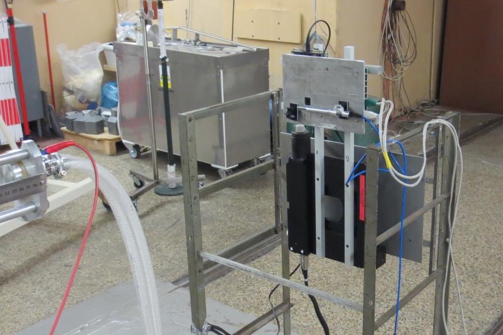
13 Irradiation Setup 13
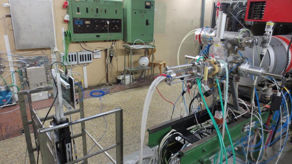
14 Irradiation Setup 14
 counted")
15 Spartan3 Irradiation Xilinx SRAM FPGA Starter Kit used XC3S200 device 90 nm CMOS technology Only SEU in configuration memory (CMem) counted 15
16 Error rate [1/s] Error rate [1/s] Spartan3 Irradiation 1,6 1,4 1,2 1 0,8 0,6 0,4 Configuration error rate vs. proton flux 34,05 MeV 28,242 MeV 18,004 MeV 0,35 0,3 0,25 0,2 0,15 0,1 Configuration error rate vs. energy 0,4 Mp/cm^2/s 2,5 Mp/cm^2/s 8,7 Mp/cm^2/s 50 Mp/cm^2/s 105 Mp/cm^2/s 0,2 0, Proton flux [Mp/cmM^2/s] Energy [MeV] 16
 17")
17 SmartFusion2 Irradiation Microsemi FLASH SoC Only FPGA part tested Starter Kit used M2S050-FGG484 device 65 nm CMOS technology No SEU in configuration memory Some SEU in data flipflops (D-FFs) 17
18 Error rate [1/s] Error rate [1/s] SmartFusion2 Irradiation D-FF error rate vs. proton flux D-FF error rate vs. energy 0,3 34,745 MeV 0,07 1 Mp/cm^2/s 0,25 28,169 MeV 0,06 8 Mp/cm^2/s 0,2 17,613 MeV 0,05 50 Mp/cm^2/s 0,04 0,15 0,03 0,1 0,02 0,05 0, Proton flux [Mp/cmM^2/s] Energy [MeV] 18
19 Current work Preparing the same test for the IGLOO2 FLASH based FPGA Precise monitoring of the total dose Upgrade the communication module Synchronization of the FPGAs clock with cyclotron frequency Improving model of architecture, collect another data and calibrate the model 19
20 Conclusions We have proposed new method for predicting quantitative characteristics of SEU sensitivity of digital circuits implemented in FPGA. We have completed the first runs of ALT. We are currently working on the simulation model, improving the ALT system and preparing the tests for other devices. This method can be used for verifying dependability and security parameters of various designs implemented in FPGA 20
21 Conclusions FLASH based SmartFusion 2 (65 nm) has better resistance to Single Event Effects than Spartan 3 (90 nm) Configuration memory completely safe D flip-flops less vulnerable, although it is a smaller technology But the SmartFusion 2 has a very low total ionizing dose to permanently destroy to destroy the FLASH programming controller. ~4 krads for SF2 Spartan 3 already survived several hundreds of krads without permanent error noticed 21
22 Digital Design and Dependability Research Group FIT, CTU in Prague Thank you! Tomáš Vaňát, Jan Pospíšil, Jan Schmidt {vanattom, Special thanks to Jozef Ferencei Department of Nuclear Spectroscopy, NPI of ASCR
Self Restoring Logic (SRL) Cell Targets Space Application Designs
 Cell Targets Space Application Designs") TND6199/D Rev. 0, SEPT 2015 Self Restoring Logic (SRL) Cell Targets Space Application Designs Semiconductor Components Industries, LLC, 2015 September, 2015 Rev. 0 1 Publication Order Number: TND6199/D
TND6199/D Rev. 0, SEPT 2015 Self Restoring Logic (SRL) Cell Targets Space Application Designs Semiconductor Components Industries, LLC, 2015 September, 2015 Rev. 0 1 Publication Order Number: TND6199/D
Field Programmable Gate Arrays (FPGAs)
") Field Programmable Gate Arrays (FPGAs) Introduction Simulations and prototyping have been a very important part of the electronics industry since a very long time now. Before heading in for the actual
Field Programmable Gate Arrays (FPGAs) Introduction Simulations and prototyping have been a very important part of the electronics industry since a very long time now. Before heading in for the actual
EECS150 - Digital Design Lecture 3 Synchronous Digital Systems Review. Announcements
 EECS150 - Digital Design Lecture 3 Synchronous Digital Systems Review September 1, 2011 Elad Alon Electrical Engineering and Computer Sciences University of California, Berkeley http://www-inst.eecs.berkeley.edu/~cs150
Single-Event Upsets in the PANDA EMC
 Single-Event Upsets in the PANDA EMC Results from a neutron irradiation of the front-end digitiser board M. Preston, P.-E. Tegnér (Stockholm University) H. Calén, T. Johansson, K. Makònyi, P. Marciniewski
Self-Test and Adaptation for Random Variations in Reliability
 Self-Test and Adaptation for Random Variations in Reliability Kenneth M. Zick and John P. Hayes University of Michigan, Ann Arbor, MI USA August 31, 2010 Motivation Physical variation is increasing dramatically
A Practical Look at SEU, Effects and Mitigation
 A Practical Look at SEU, Effects and Mitigation Ken Chapman FPGA Network: Safety, Certification & Security University of Hertfordshire 19 th May 2016 Premium Bonds Each Bond is 1 Each stays in the system
EITF35: Introduction to Structured VLSI Design
 EITF35: Introduction to Structured VLSI Design Part 4.2.1: Learn More Liang Liu liang.liu@eit.lth.se 1 Outline Crossing clock domain Reset, synchronous or asynchronous? 2 Why two DFFs? 3 Crossing clock
Tutorial 11 ChipscopePro, ISE 10.1 and Xilinx Simulator on the Digilent Spartan-3E board
 Tutorial 11 ChipscopePro, ISE 10.1 and Xilinx Simulator on the Digilent Spartan-3E board Introduction This lab will be an introduction on how to use ChipScope for the verification of the designs done on
Impact of Intermittent Faults on Nanocomputing Devices
 Impact of Intermittent Faults on Nanocomputing Devices Cristian Constantinescu June 28th, 2007 Dependable Systems and Networks Outline Fault classes Permanent faults Transient faults Intermittent faults
High Density Asynchronous LUT Based on Non-Volatile MRAM Technology
 20th International Conference on Field Programmable Logic and Applications Milano, ITALY, Aug. 31st - Sep. 2nd, 2010 High Density Asynchronous LUT Based on Non-Volatile MRAM Technology Sumanta Chaudhuri,
Modeling Latches and Flip-flops
 Lab Workbook Introduction Sequential circuits are digital circuits in which the output depends not only on the present input (like combinatorial circuits), but also on the past sequence of inputs. In effect,
March 13, :36 vra80334_appe Sheet number 1 Page number 893 black. appendix. Commercial Devices
 March 13, 2007 14:36 vra80334_appe Sheet number 1 Page number 893 black appendix E Commercial Devices In Chapter 3 we described the three main types of programmable logic devices (PLDs): simple PLDs, complex
Lecture 2: Basic FPGA Fabric. James C. Hoe Department of ECE Carnegie Mellon University
 18 643 Lecture 2: Basic FPGA Fabric James. Hoe Department of EE arnegie Mellon University 18 643 F17 L02 S1, James. Hoe, MU/EE/ALM, 2017 Housekeeping Your goal today: know enough to build a basic FPGA
Chapter 5 Flip-Flops and Related Devices
 Chapter 5 Flip-Flops and Related Devices Chapter 5 Objectives Selected areas covered in this chapter: Constructing/analyzing operation of latch flip-flops made from NAND or NOR gates. Differences of synchronous/asynchronous
Lecture 6: Simple and Complex Programmable Logic Devices. EE 3610 Digital Systems
 EE 3610: Digital Systems 1 Lecture 6: Simple and Complex Programmable Logic Devices MEMORY 2 Volatile: need electrical power Nonvolatile: magnetic disk, retains its stored information after the removal
Sequential Logic. E&CE 223 Digital Circuits and Systems (A. Kennings) Page 1
 Page 1") Sequential Logic E&CE 223 igital Circuits and Systems (A. Kennings) Page 1 Sequential Circuits Have considered only combinational circuits in which circuit outputs are determined entirely by current circuit
Sequential Logic E&CE 223 igital Circuits and Systems (A. Kennings) Page 1 Sequential Circuits Have considered only combinational circuits in which circuit outputs are determined entirely by current circuit
Scan. This is a sample of the first 15 pages of the Scan chapter.
 Scan This is a sample of the first 15 pages of the Scan chapter. Note: The book is NOT Pinted in color. Objectives: This section provides: An overview of Scan An introduction to Test Sequences and Test
FPGA Design. Part I - Hardware Components. Thomas Lenzi
 FPGA Design Part I - Hardware Components Thomas Lenzi Approach We believe that having knowledge of the hardware components that compose an FPGA allow for better firmware design. Being able to visualise
Single Event Characterization of a Xilinx UltraScale+ MP-SoC FPGA
 Single Event Characterization of a Xilinx UltraScale+ MP-SoC FPGA Thomas LANGE, Maximilien GLORIEUX, Adrian EVANS, A-Duong IN, Thierry BONNOIT, Dan ALEXANDRESCU iroc Technologies France Cesar BOATELLA
Clarke and Inverse ClarkeTransformations Hardware Implementation. User Guide
 Clarke and Inverse ClarkeTransformations Hardware Implementation User Guide Clarke and Inverse Clarke Transformations Hardware Implementation User Guide Table of Contents Clarke and Inverse Clarke Transformations
Synchronization Voter Insertion Algorithms for FPGA Designs Using Triple Modular Redundancy
 Brigham Young University BYU ScholarsArchive All Theses and Dissertations 2010-03-10 Synchronization Voter Insertion Algorithms for FPGA Designs Using Triple Modular Redundancy Jonathan Mark Johnson Brigham
FPGA Design with VHDL
 FPGA Design with VHDL Justus-Liebig-Universität Gießen, II. Physikalisches Institut Ming Liu Dr. Sören Lange Prof. Dr. Wolfgang Kühn ming.liu@physik.uni-giessen.de Lecture Digital design basics Basic logic
Examples of FPLD Families: Actel ACT, Xilinx LCA, Altera MAX 5000 & 7000
 Examples of FPL Families: Actel ACT, Xilinx LCA, Altera AX 5 & 7 Actel ACT Family ffl The Actel ACT family employs multiplexer-based logic cells. ffl A row-based architecture is used in which the logic
Investigation of Look-Up Table Based FPGAs Using Various IDCT Architectures
 Investigation of Look-Up Table Based FPGAs Using Various IDCT Architectures Jörn Gause Abstract This paper presents an investigation of Look-Up Table (LUT) based Field Programmable Gate Arrays (FPGAs)
Why FPGAs? FPGA Overview. Why FPGAs?
 Transistor-level Logic Circuits Positive Level-sensitive EECS150 - Digital Design Lecture 3 - Field Programmable Gate Arrays (FPGAs) January 28, 2003 John Wawrzynek Transistor Level clk clk clk Positive
FPGA Based Implementation of Convolutional Encoder- Viterbi Decoder Using Multiple Booting Technique
 FPGA Based Implementation of Convolutional Encoder- Viterbi Decoder Using Multiple Booting Technique Dr. Dhafir A. Alneema (1) Yahya Taher Qassim (2) Lecturer Assistant Lecturer Computer Engineering Dept.
Reduced Triple Modular Redundancy for Tolerating SEUs in SRAM-based FPGAs
 Reduced Triple Modular Redundancy for Tolerating SEUs in SRAM-based FPGAs Vikram Chandrasekhar Sk Noor Mahammad V Muralidaran V Kamakoti Department of Computer Science and Engineering Indian Institute
VHDL Design and Implementation of FPGA Based Logic Analyzer: Work in Progress
 VHDL Design and Implementation of FPGA Based Logic Analyzer: Work in Progress Nor Zaidi Haron Ayer Keroh +606-5552086 zaidi@utem.edu.my Masrullizam Mat Ibrahim Ayer Keroh +606-5552081 masrullizam@utem.edu.my
A Tool For Run Time Soft Error Fault Injection. Into FPGA Circuits
 A Tool For Run Time Soft Error Fault Injection Into FPGA Circuits A TOOL FOR RUN TIME SOFT ERROR FAULT INJECTION INTO FPGA CIRCUITS BY MARVIN ZUZARTE, B.Eng. a thesis submitted to the department of Computing
2.6 Reset Design Strategy
 2.6 Reset esign Strategy Many design issues must be considered before choosing a reset strategy for an ASIC design, such as whether to use synchronous or asynchronous resets, will every flipflop receive
CSE140L: Components and Design Techniques for Digital Systems Lab. CPU design and PLDs. Tajana Simunic Rosing. Source: Vahid, Katz
 CSE140L: Components and Design Techniques for Digital Systems Lab CPU design and PLDs Tajana Simunic Rosing Source: Vahid, Katz 1 Lab #3 due Lab #4 CPU design Today: CPU design - lab overview PLDs Updates
FPGA Implementation of DA Algritm for Fir Filter
 International Journal of Computational Engineering Research Vol, 03 Issue, 8 FPGA Implementation of DA Algritm for Fir Filter 1, Solmanraju Putta, 2, J Kishore, 3, P. Suresh 1, M.Tech student,assoc. Prof.,Professor
An Introduction to Radiation-Induced Failure Modes and Related Mitigation Methods For Xilinx SRAM FPGAs
 n Introduction to Radiation-Induced Failure Modes and Related Mitigation Methods For Xilinx SRM FPGs Heather Quinn, Paul Graham, Keith Morgan, Jim Krone, Michael Caffrey, and Michael Wirthlin bstract Over
Reconfigurable Architectures. Greg Stitt ECE Department University of Florida
 Reconfigurable Architectures Greg Stitt ECE Department University of Florida How can hardware be reconfigurable? Problem: Can t change fabricated chip ASICs are fixed Solution: Create components that can
Voter Insertion Techniques for Fault Tolerant FPGA Design.
 Voter Insertion Techniques for Fault Tolerant FPGA Design. Jonathan Johnson Michael Wirthlin NSF Center for High Performance Reconfigurable Computing (CHREC) Dept. of Elec. & Comp. Engineering Brigham
Total Ionizing Dose Test Report. No. 14T-RTSX32SU-CQ256-D1RH41
 Total Ionizing Dose Test Report No. 14T-RTSX32SU-CQ256-D1RH41 March 9, 2014 Table of Contents I. Summary Table... 3 II. Total Ionizing Dose (TID) Testing... 3 A. Device-Under-Test (DUT) and Irradiation
L11/12: Reconfigurable Logic Architectures
 L11/12: Reconfigurable Logic Architectures Acknowledgements: Materials in this lecture are courtesy of the following people and used with permission. - Randy H. Katz (University of California, Berkeley,
Irradiation Resistivity and Mitigation Measurement Design for Xilinx Kintex-7 FPGAs
 Irradiation Resistivity and Mitigation Measurement Design for Xilinx Kintex-7 FPGAs Master Thesis in Microelectronics Lukas On Arnold Institute of Microelectronics, School of Engineering, University of
L12: Reconfigurable Logic Architectures
 L12: Reconfigurable Logic Architectures Acknowledgements: Materials in this lecture are courtesy of the following sources and are used with permission. Frank Honore Prof. Randy Katz (Unified Microelectronics
CSE140L: Components and Design Techniques for Digital Systems Lab. FSMs. Tajana Simunic Rosing. Source: Vahid, Katz
 CSE140L: Components and Design Techniques for Digital Systems Lab FSMs Tajana Simunic Rosing Source: Vahid, Katz 1 Flip-flops Hardware Description Languages and Sequential Logic representation of clocks
Digital Integrated Circuits EECS 312
 14 12 10 8 6 Fujitsu VP2000 IBM 3090S Pulsar 4 IBM 3090 IBM RY6 CDC Cyber 205 IBM 4381 IBM RY4 2 IBM 3081 Apache Fujitsu M380 IBM 370 Merced IBM 360 IBM 3033 Vacuum Pentium II(DSIP) 0 1950 1960 1970 1980
RTG4 Radiation Update J.J. Wang, Chief Engineer Nadia Rezzak, Staff Engineer Stephen Varela, Engineer
 RTG4 Radiation Update J.J. Wang, Chief Engineer Nadia Rezzak, Staff Engineer Stephen Varela, Engineer 1 Company Overview Leading-Edge Semiconductor Solutions Differentiated by: Performance Reliability
Product Update. JTAG Issues and the Use of RT54SX Devices
 Product Update Revision Date: September 2, 999 JTAG Issues and the Use of RT54SX Devices BACKGROUND The attached paper authored by Richard B. Katz of NASA GSFC and J. J. Wang of Actel describes anomalies
Introduction Actel Logic Modules Xilinx LCA Altera FLEX, Altera MAX Power Dissipation
 Outline CPE 528: Session #12 Department of Electrical and Computer Engineering University of Alabama in Huntsville Introduction Actel Logic Modules Xilinx LCA Altera FLEX, Altera MAX Power Dissipation
Unit 11. Latches and Flip-Flops
 Unit 11 Latches and Flip-Flops 1 Combinational Circuits A combinational circuit consists of logic gates whose outputs, at any time, are determined by combining the values of the inputs. For n input variables,
Lecture 8: Sequential Logic
 Lecture 8: Sequential Logic Last lecture discussed how we can use digital electronics to do combinatorial logic we designed circuits that gave an immediate output when presented with a given set of inputs
EL302 DIGITAL INTEGRATED CIRCUITS LAB #3 CMOS EDGE TRIGGERED D FLIP-FLOP. Due İLKER KALYONCU, 10043
 EL302 DIGITAL INTEGRATED CIRCUITS LAB #3 CMOS EDGE TRIGGERED D FLIP-FLOP Due 16.05. İLKER KALYONCU, 10043 1. INTRODUCTION: In this project we are going to design a CMOS positive edge triggered master-slave
Register Files and Memories
 Register Files and Memories ECE 554 Digital Engineering Laboratory C. R. Kime 2/18/2002 Register Files and Memories Register Files Issues and Objectives Register File Concepts Implementation of Register
An Application Specific Reconfigurable Architecture Diagnosis Fault in the LUT of Cluster Based FPGA
 An Application Specific Reconfigurable Architecture Diagnosis Fault in the LUT of Cluster Based FPGA Abstract: The increased circuit complexity of field programmable gate array (FPGA) poses a major challenge
https://daffy1108.wordpress.com/2014/06/08/synchronizers-for-asynchronous-signals/
 https://daffy1108.wordpress.com/2014/06/08/synchronizers-for-asynchronous-signals/ Synchronizers for Asynchronous Signals Asynchronous signals causes the big issue with clock domains, namely metastability.
Modeling Latches and Flip-flops
 Lab Workbook Introduction Sequential circuits are the digital circuits in which the output depends not only on the present input (like combinatorial circuits), but also on the past sequence of inputs.
Faculty of Electrical & Electronics Engineering BEE3233 Electronics System Design. Laboratory 3: Finite State Machine (FSM)
") Faculty of Electrical & Electronics Engineering BEE3233 Electronics System Design Laboratory 3: Finite State Machine (FSM) Mapping CO, PO, Domain, KI : CO2,PO3,P5,CTPS5 CO2: Construct logic circuit using
Faculty of Electrical & Electronics Engineering BEE3233 Electronics System Design Laboratory 3: Finite State Machine (FSM) Mapping CO, PO, Domain, KI : CO2,PO3,P5,CTPS5 CO2: Construct logic circuit using
Overview: Logic BIST
 VLSI Design Verification and Testing Built-In Self-Test (BIST) - 2 Mohammad Tehranipoor Electrical and Computer Engineering University of Connecticut 23 April 2007 1 Overview: Logic BIST Motivation Built-in
An Application Specific Reconfigurable Architecture Diagnosis Fault in the LUT of Cluster Based FPGA
 International Journal of Innovative Research in Electronics and Communications (IJIREC) Volume 2, Issue 5, July 2015, PP 1-7 ISSN 2349-4042 (Print) & ISSN 2349-4050 (Online) www.arcjournals.org An Application
More on Flip-Flops Digital Design and Computer Architecture: ARM Edition 2015 Chapter 3 <98> 98
 More on Flip-Flops Digital Design and Computer Architecture: ARM Edition 2015 Chapter 3 98 Review: Bit Storage SR latch S (set) Q R (reset) Level-sensitive SR latch S S1 C R R1 Q D C S R D latch Q
Sequential Design Basics
 Sequential Design Basics Lecture 2 topics A review of devices that hold state A review of Latches A review of Flip-Flops Unit of text Set-Reset Latch/Flip-Flops/D latch/ Edge triggered D Flip-Flop 8/22/22
Read-only memory (ROM) Digital logic: ALUs Sequential logic circuits. Don't cares. Bus
 Digital logic: ALUs Sequential logic circuits. Don't cares. Bus") Digital logic: ALUs Sequential logic circuits CS207, Fall 2004 October 11, 13, and 15, 2004 1 Read-only memory (ROM) A form of memory Contents fixed when circuit is created n input lines for 2 n addressable
Digital logic: ALUs Sequential logic circuits CS207, Fall 2004 October 11, 13, and 15, 2004 1 Read-only memory (ROM) A form of memory Contents fixed when circuit is created n input lines for 2 n addressable
Neutron Irradiation Tests of an S-LINK-over-G-link System
 Nov. 21, 1999 Neutron Irradiation Tests of an S-LINK-over-G-link System K. Anderson, J. Pilcher, H. Wu Enrico Fermi Institute, University of Chicago, Chicago, IL E. van der Bij, Z. Meggyesi EP/ATE Division,
Design of a Low Power Four-Bit Binary Counter Using Enhancement Type Mosfet
 Design of a Low Power Four-Bit Binary Counter Using Enhancement Type Mosfet Praween Sinha Department of Electronics & Communication Engineering Maharaja Agrasen Institute Of Technology, Rohini sector -22,
A NOVEL DESIGN OF COUNTER USING TSPC D FLIP-FLOP FOR HIGH PERFORMANCE AND LOW POWER VLSI DESIGN APPLICATIONS USING 45NM CMOS TECHNOLOGY
 A NOVEL DESIGN OF COUNTER USING TSPC D FLIP-FLOP FOR HIGH PERFORMANCE AND LOW POWER VLSI DESIGN APPLICATIONS USING 45NM CMOS TECHNOLOGY Ms. Chaitali V. Matey 1, Ms. Shraddha K. Mendhe 2, Mr. Sandip A.
DESIGNING AN ECU CPU FOR RADIATION ENVIRONMENT. Matthew G. M. Yee College of Engineering University of Hawai`i at Mānoa Honolulu, HI ABSTRACT
 DESIGNING AN ECU CPU FOR RADIATION ENVIRONMENT Matthew G. M. Yee College of Engineering University of Hawai`i at Mānoa Honolulu, HI 96822 ABSTRACT NASA s objective is to colonize the planet Mars, for the
LOW POWER AND HIGH PERFORMANCE SHIFT REGISTERS USING PULSED LATCH TECHNIQUE
 OI: 10.21917/ijme.2018.0088 LOW POWER AN HIGH PERFORMANCE SHIFT REGISTERS USING PULSE LATCH TECHNIUE Vandana Niranjan epartment of Electronics and Communication Engineering, Indira Gandhi elhi Technical
VGA Controller. Leif Andersen, Daniel Blakemore, Jon Parker University of Utah December 19, VGA Controller Components
 VGA Controller Leif Andersen, Daniel Blakemore, Jon Parker University of Utah December 19, 2012 Fig. 1. VGA Controller Components 1 VGA Controller Leif Andersen, Daniel Blakemore, Jon Parker University
Lab #10 Hexadecimal-to-Seven-Segment Decoder, 4-bit Adder-Subtractor and Shift Register. Fall 2017
 University of Texas at El Paso Electrical and Computer Engineering Department EE 2169 Laboratory for Digital Systems Design I Lab #10 Hexadecimal-to-Seven-Segment Decoder, 4-bit Adder-Subtractor and Shift
CAD for VLSI Design - I Lecture 38. V. Kamakoti and Shankar Balachandran
 1 CAD for VLSI Design - I Lecture 38 V. Kamakoti and Shankar Balachandran 2 Overview Commercial FPGAs Architecture LookUp Table based Architectures Routing Architectures FPGA CAD flow revisited 3 Xilinx
Performance Driven Reliable Link Design for Network on Chips
 Performance Driven Reliable Link Design for Network on Chips Rutuparna Tamhankar Srinivasan Murali Prof. Giovanni De Micheli Stanford University Outline Introduction Objective Logic design and implementation
Chapter 7 Memory and Programmable Logic
 EEA091 - Digital Logic 數位邏輯 Chapter 7 Memory and Programmable Logic 吳俊興國立高雄大學資訊工程學系 2006 Chapter 7 Memory and Programmable Logic 7-1 Introduction 7-2 Random-Access Memory 7-3 Memory Decoding 7-4 Error
RELATED WORK Integrated circuits and programmable devices
 Chapter 2 RELATED WORK 2.1. Integrated circuits and programmable devices 2.1.1. Introduction By the late 1940s the first transistor was created as a point-contact device formed from germanium. Such an
VID_OVERLAY. Digital Video Overlay Module Rev Key Design Features. Block Diagram. Applications. Pin-out Description
 Key Design Features Block Diagram Synthesizable, technology independent VHDL IP Core Video overlays on 24-bit RGB or YCbCr 4:4:4 video Supports all video resolutions up to 2 16 x 2 16 pixels Supports any
Introduction. NAND Gate Latch. Digital Logic Design 1 FLIP-FLOP. Digital Logic Design 1
 2007 Introduction BK TP.HCM FLIP-FLOP So far we have seen Combinational Logic The output(s) depends only on the current values of the input variables Here we will look at Sequential Logic circuits The
Experiment # 12. Traffic Light Controller
 Experiment # 12 Traffic Light Controller Objectives Practice on the design of clocked sequential circuits. Applications of sequential circuits. Overview In this lab you are going to develop a Finite State
data and is used in digital networks and storage devices. CRC s are easy to implement in binary
 Introduction Cyclic redundancy check (CRC) is an error detecting code designed to detect changes in transmitted data and is used in digital networks and storage devices. CRC s are easy to implement in
Testing Sequential Logic. CPE/EE 428/528 VLSI Design II Intro to Testing (Part 2) Testing Sequential Logic (cont d) Testing Sequential Logic (cont d)
 Testing Sequential Logic (cont d) Testing Sequential Logic (cont d)") Testing Sequential Logic CPE/EE 428/528 VLSI Design II Intro to Testing (Part 2) Electrical and Computer Engineering University of Alabama in Huntsville In general, much more difficult than testing combinational
Testing Sequential Logic CPE/EE 428/528 VLSI Design II Intro to Testing (Part 2) Electrical and Computer Engineering University of Alabama in Huntsville In general, much more difficult than testing combinational
Engr354: Digital Logic Circuits
 Engr354: igital Circuits Chapter 7 Sequential Elements r. Curtis Nelson Sequential Elements In this chapter you will learn about: circuits that can store information; Basic cells, latches, and flip-flops;
Single-Event Upset Technology Scaling Trends of. Unhardened and Hardened Flip-Flops in Bulk CMOS. Nelson J. Gaspard III.
 Single-Event Upset Technology Scaling Trends of Unhardened and Hardened Flip-Flops in Bulk CMOS By Nelson J. Gaspard III Dissertation Submitted to the Faculty of the Graduate School of Vanderbilt University
Implementation of Dynamic RAMs with clock gating circuits using Verilog HDL
 Implementation of Dynamic RAMs with clock gating circuits using Verilog HDL B.Sanjay 1 SK.M.Javid 2 K.V.VenkateswaraRao 3 Asst.Professor B.E Student B.E Student SRKR Engg. College SRKR Engg. College SRKR
True Random Number Generation with Logic Gates Only
 True Random Number Generation with Logic Gates Only Jovan Golić Security Innovation, Telecom Italia Winter School on Information Security, Finse 2008, Norway Jovan Golic, Copyright 2008 1 Digital Random
Radiation Effects and Mitigation Techniques for FPGAs
 Radiation Effects and Mitigation Techniques for FPGAs Fernanda Lima Kastensmidt Universidade Federal do Rio Grande do Sul (UFRGS) Contact: fglima@inf.ufrgs.br Field Programmable Gate Arrays A type of gate
YEDITEPE UNIVERSITY DEPARTMENT OF COMPUTER ENGINEERING. EXPERIMENT VIII: FLIP-FLOPS, COUNTERS 2014 Fall
 YEDITEPE UNIVERSITY DEPARTMENT OF COMPUTER ENGINEERING EXPERIMENT VIII: FLIP-FLOPS, COUNTERS 2014 Fall Objective: - Dealing with the operation of simple sequential devices. Learning invalid condition in
HARDENED BY DESIGN APPROACHES FOR MITIGATING TRANSIENT FAULTS IN MEMORY-BASED SYSTEMS DANIEL RYAN BLUM
 HARDENED BY DESIGN APPROACHES FOR MITIGATING TRANSIENT FAULTS IN MEMORY-BASED SYSTEMS by DANIEL RYAN BLUM A dissertation submitted in partial fulfillment of the requirements for the degree of DOCTOR OF
Design Techniques for Radiation-Hardened FPGAs
 Design Techniques for Radiation-Hardened FPGAs Application Note AC128 Introduction With the RH1280 and RH1020, Actel Corporation introduces radiation-hardened versions of the popular A1280 and A1020 field
Chapter 6. Flip-Flops and Simple Flip-Flop Applications
 Chapter 6 Flip-Flops and Simple Flip-Flop Applications Basic bistable element It is a circuit having two stable conditions (states). It can be used to store binary symbols. J. C. Huang, 2004 Digital Logic
Jin-Fu Li Advanced Reliable Systems (ARES) Laboratory. National Central University
 Laboratory. National Central University") Chapter 3 Basics of VLSI Testing (2) Jin-Fu Li Advanced Reliable Systems (ARES) Laboratory Department of Electrical Engineering National Central University Jhongli, Taiwan Outline Testing Process Fault
Chapter 3 Basics of VLSI Testing (2) Jin-Fu Li Advanced Reliable Systems (ARES) Laboratory Department of Electrical Engineering National Central University Jhongli, Taiwan Outline Testing Process Fault
Unit 9 Latches and Flip-Flops. Dept. of Electrical and Computer Eng., NCTU 1
 Unit 9 Latches and Flip-Flops Dept. of Electrical and Computer Eng., NCTU 1 9.1 Introduction Dept. of Electrical and Computer Eng., NCTU 2 What is the characteristic of sequential circuits in contrast
Figure 1 Block diagram of a 4-bit binary counter
 Lab 3: Four-Bit Binary Counter EE-459/500 HDL Based Digital Design with Programmable Logic Electrical Engineering Department, University at Buffalo Last update: Cristinel Ababei, August 2012 1. Objective
FPGA-BASED EDUCATIONAL LAB PLATFORM
 FPGA-BASED EDUCATIONAL LAB PLATFORM Mircea Alexandru DABÂCAN, Clint COLE Mircea Dabâcan is with Technical University of Cluj-Napoca, Electronics and Telecommunications Faculty, Applied Electronics Department,
DEPARTMENT OF ELECTRICAL &ELECTRONICS ENGINEERING DIGITAL DESIGN
 DEPARTMENT OF ELECTRICAL &ELECTRONICS ENGINEERING DIGITAL DESIGN Assoc. Prof. Dr. Burak Kelleci Spring 2018 OUTLINE Synchronous Logic Circuits Latch Flip-Flop Timing Counters Shift Register Synchronous
Level and edge-sensitive behaviour
 Level and edge-sensitive behaviour Asynchronous set/reset is level-sensitive Include set/reset in sensitivity list Put level-sensitive behaviour first: process (clock, reset) is begin if reset = '0' then
EET2411 DIGITAL ELECTRONICS
 5-8 Clocked D Flip-FlopFlop One data input. The output changes to the value of the input at either the positive going or negative going clock trigger. May be implemented with a J-K FF by tying the J input
AbhijeetKhandale. H R Bhagyalakshmi
 Sobel Edge Detection Using FPGA AbhijeetKhandale M.Tech Student Dept. of ECE BMS College of Engineering, Bangalore INDIA abhijeet.khandale@gmail.com H R Bhagyalakshmi Associate professor Dept. of ECE BMS
Chapter 8 Design for Testability
 電機系 Chapter 8 Design for Testability 測試導向設計技術 2 Outline Introduction Ad-Hoc Approaches Full Scan Partial Scan 3 Design For Testability Definition Design For Testability (DFT) refers to those design techniques
Bit Swapping LFSR and its Application to Fault Detection and Diagnosis Using FPGA
 Bit Swapping LFSR and its Application to Fault Detection and Diagnosis Using FPGA M.V.M.Lahari 1, M.Mani Kumari 2 1,2 Department of ECE, GVPCEOW,Visakhapatnam. Abstract The increasing growth of sub-micron
Report on 4-bit Counter design Report- 1, 2. Report on D- Flipflop. Course project for ECE533
 Report on 4-bit Counter design Report- 1, 2. Report on D- Flipflop Course project for ECE533 I. Objective: REPORT-I The objective of this project is to design a 4-bit counter and implement it into a chip
LFSRs as Functional Blocks in Wireless Applications Author: Stephen Lim and Andy Miller
 XAPP22 (v.) January, 2 R Application Note: Virtex Series, Virtex-II Series and Spartan-II family LFSRs as Functional Blocks in Wireless Applications Author: Stephen Lim and Andy Miller Summary Linear Feedback
PROCESSOR BASED TIMING SIGNAL GENERATOR FOR RADAR AND SENSOR APPLICATIONS
 PROCESSOR BASED TIMING SIGNAL GENERATOR FOR RADAR AND SENSOR APPLICATIONS Application Note ABSTRACT... 3 KEYWORDS... 3 I. INTRODUCTION... 4 II. TIMING SIGNALS USAGE AND APPLICATION... 5 III. FEATURES AND
Reconfigurable FPGA Implementation of FIR Filter using Modified DA Method
 Reconfigurable FPGA Implementation of FIR Filter using Modified DA Method M. Backia Lakshmi 1, D. Sellathambi 2 1 PG Student, Department of Electronics and Communication Engineering, Parisutham Institute
6. Sequential Logic Flip-Flops
 ection 6. equential Logic Flip-Flops Page of 5 6. equential Logic Flip-Flops ombinatorial components: their output values are computed entirely from their present input values. equential components: their
Sharif University of Technology. SoC: Introduction
 SoC Design Lecture 1: Introduction Shaahin Hessabi Department of Computer Engineering System-on-Chip System: a set of related parts that act as a whole to achieve a given goal. A system is a set of interacting
Digital Circuits ECS 371
 igital Circuits ECS 371 r. Prapun Suksompong prapun@siit.tu.ac.th Lecture 17 Office Hours: BK 3601-7 Monday 9:00-10:30, 1:30-3:30 Tuesday 10:30-11:30 1 Announcement Reading Assignment: Chapter 7: 7-1,
Combinational vs Sequential
 Combinational vs Sequential inputs X Combinational Circuits outputs Z A combinational circuit: At any time, outputs depends only on inputs Changing inputs changes outputs No regard for previous inputs