Chap. 5 Flip-Flops and Related Devices
|
|
|
- Marsha Adams
- 5 years ago
- Views:
Transcription
1 5- Introduction Combinational Circuit The output levels at any instant of time are dependent on the levels present at the inputs at that time» Any prior input-level conditions have no effect on the present outputs because combinational logic circuits have no memory Most = Combinational circuits + Memory elements General digital system that combines combinational logic gates with memory device : Fig. 5-» The external outputs are a function of both its external inputs and the information stored in its memory elements The most important memory element = Flip-Flop F/F is made up of an assembly of logic gates : Feedback» Even though a logic gate, by itself, has no storage capability, several can be connected together in ways that permit information to be stored(refer to Fig. 5-7). Output State of F/F : Fig. 5-2 Normal output () : or = HIGH = Set Inverted output() : or = LOW = Clear = Reset F/F = Latch = Bistable multivibrator (Refer to Slide 5-28). F/F : Clock Edge Sensitive Latch : Level Sensitive
2 NAND Gate Latch NAND gate latch(or Latch) Fig. 5-3 참고 Normal rest Constructed from two NAND gates : Fig. 5-3 Setting the Latch Both cases ends up HIGH : Fig. 5-4 Clearing the Latch Both cases ends up LOW : Fig. 5-5 Simultaneous Setting and Clearing Set = Clear =» = = : Undesired condition Set = Clear =» No change NAND Latch Summary Fig. 5-6(a),(b) Normally High Input Set Clear Output No change = = Invalid Fig. 5-3 Fig. 5-4 Fig. 5-5 SET CLEAR SET CLEAR Fig possible resting state when SET=RESET= SET CLEAR SET CLEAR SET SET CLEAR Fig. 5-4 Pulsing SET input to CLEAR Fig. 5-5 Pulsing CLEAR input to
3 5-3 Alternate Representations : Fig. 5-7 Ex. 5-) Determine output in Fig. 5-8 Ex. 5-2) Switch debouncing circuit in Fig NOR gate Latch Resting Input = Ex. 5-4 SW Ex. 5-3) Determine output in Fig. 5- Ex. 5-4) What happen if the light beam is momentarily interrupted in Fig. 5-2 will remain HIGH and the alarm will remain ON even if phototransistor return to ON ( Set=, Clear= : no change) F/F State on Power-Up Set Clear Output No change = = Invalid Set Clear Output No change = = Invalid Fig. 5- (a) NOR gate latch, (b) truth table, (c) simplified block symbol When power is on, not possible to predict the starting state of a F/F s output Output depend on factors such as internal propagation delays, parasitic capacitance, and external loading. To start of in a particular state, activate SET/CLEAR input at the start of circuit. SET CLEAR * Inactive Stage(Resting ) NAND latch : S=C= NOR latch : S=C= S R Fig. 5-7 Alternate Representation * Invalid = =
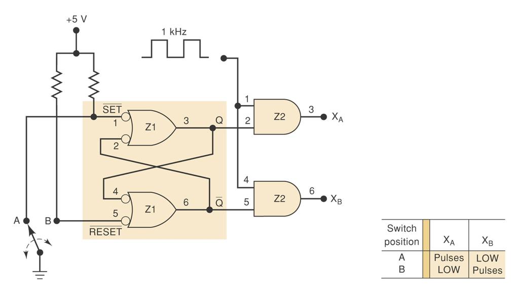
4 Troubleshooting Case Study Ex. 5-5) Describe & analyze the circuit in Fig. 5-3 Ex. 5-6) What are the possible faults(refer to Tab. 5-) Possible faults(switch position A에서 Fault : =이여야함 )» Internal open at Z- : 이입력되지않음 SET=RESET=» Component failure in NAND gate Z» Internally shorted to ground at Z-3, Z-4, and Z2-2» Node externally shorted to ground 5-4 Digital Pulses Pulse A signal switches from a normal inactive state to the opposite (active) state, then the signal returns to its inactive state. Positive pulse Performs its intended function when it goes HIGH : Fig. 5-4(a) Negative pulse Performs its intended function when it goes LOW : Fig. 5-4(b) Rise time t r / Fall time t f The time it takes the voltage to change between % and 9% Refer to Fig. 5-4(a), (b)
5 5-5 Fig. 5-3 : Example 5-5 and 5-6
6 5-6 Leading edge The transition at the beginning of the pulse Trailing edge The transition at the end of the pulse Pulse width tw The time between the points when the leading and trailing edges are at 5% Ex. 5-7) Draw a scaled drawing of the RD pulse. : Fig Clock Signals and Clocked F/Fs Async/Synchronous System Asynchronous System : The output of logic circuits can change state any time Synchronous System : The exact times at which any output can change states are determined by a signal commonly called the clock» Synchronous circuits are easier to design and troubleshoot because the circuit outputs can change only at specific instants of time. Clock Signal = rectangular pulse train or square wave(fig. 5-6) Positive-Going Transition(PGT), Negative-Going Transition(NGT) The synchronizing action of the clock signals is accomplished through the use of clocked flip-flops
7 5-7
8 5-8 Clocked Flip-Flops : Fig Clocked FFs have a clock input(clk, CK, or CP)» In most clocked FFs, the CLK input is edge-triggered : NGT or PGT 2. Clocked FFs have one or more control inputs» The control inputs will have no effect on until the active clock transition occurs(=synchronous control inputs) 3. In summary,» The control inputs control the WHAT : Output state(data or ) will go to» The clock input determines the WHEN : actually triggers the change Setup and Hold Times : Fig. 5-8 Setup time(5-5 ns)» minimum time that control input must remain at constant value before the transition. Hold time( - ns)» minimum time that control input must not change after the positive transition 5-6 Clocked S-C F/F Clocked S-C F/F Set-Clear F/F Waveform analysis in Fig. 5-9 : positive going edge transition Fig % t s t h Positive clock transition Control Input Clock Input
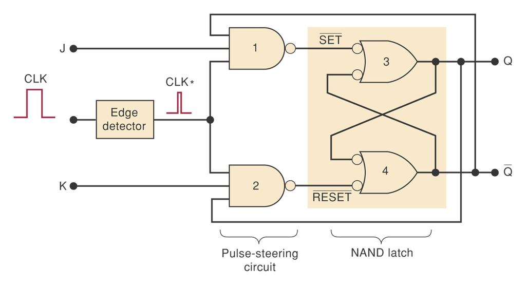
9 5-9 The clock input = Trigger input Negative-going edge transition : Fig. 5-2 Internal circuitry of the edge-triggered S-C F/F Edge-triggered S-C F/F : Fig. 5-2». NAND Latch» 2. Pulse-steering : NAND gate에모두이입력되면 SET/CLEAR= 이되고=/» 3. Edge-detector : Fig Clocked J-K F/F Jack-King F/F Clocked J-K F/F : Fig Toggle Mode : J = K = (S-C F/F 에서는 Invalid) Negative-going edge transition : Fig Internal circuitry of the edge-triggered J-K F/F : Fig =, = 인상태에서 J=K=이입력되면 5-8 Clocked D F/F» NAND 의입력은모두 이고따라서출력은 이되고 =로 Toggle» NAND 2의입력은,, 이고따라서출력은 이되고 =으로 Toggle Clocked D F/F : Fig Data F/F Implementation of the D F/F : Fig Parallel Data Transfer : Fig. 5-28

10 5- PGT NGT

11 5- Fig ns
12 5-2 x
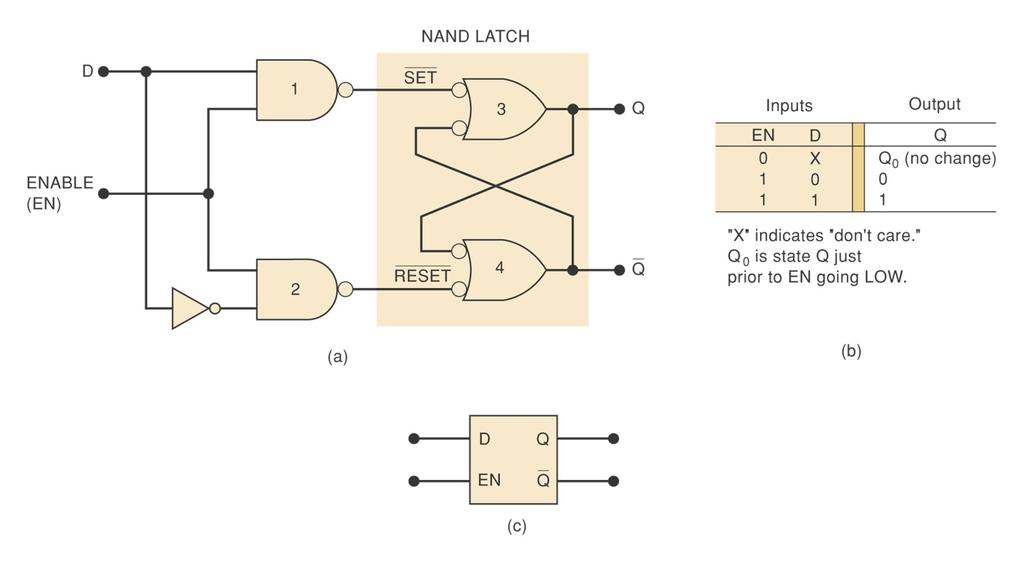
13 D Latch : Transparent Latch D Latch : Fig Edge detector is not used : EN(Enable) input 사용 Ex. 5-8) Determine waveform in Fig Asynchronous Inputs Asynchronous Inputs(= override inputs) Used to set the FF to the or clear the FF to the state at any time, regardless of the conditions at the other inputs Clocked J-K F/F with asynchronous inputs : Fig. 5-3 Designations for Asynchronous Inputs PRE(Preset), CLR(Clear) S D (Direct SET), R D (Direct RESET) Ex. 5-9) Determine the output in Fig D Latch is not Edge Triggered, (Level Triggered) Use the overbar to indicate the active LOW
14 5-4

15 5-5
16 IEEE/ANSI Symbols : deleted in th Ed. A single edge-triggered J-K flip-flop : Fig. 5-33(a) 74LS2 dual edge-triggered J-K flip-flop : Fig. 5-33(b) A single edge-triggered D flip-flop : Fig. 5-34(a) 74HC75 quad D flip-flop common clock and clear : Fig. 5-34(b) 5- F/F Timing Considerations Setup/Hold Time : slide # 5-8 Propagation Delays : Fig (Typ. MAX Few - ns) t PLH : Delay going from LOW to HIGH, t PHL : HIGH to LOW 5% CLK t PLH t PHL
17 5-7 Maximum Clock Frequency : f MAX (Typ. Max 2 to 35 MHz) Clock Pulse HIGH and LOW Times : Fig. 5-34(a) The minimum time duration that the CLK must remain LOW before it goes HIGH t W (L), and HIGH before it returns LOW t W (H) Asynchronous Active Pulse Width : Fig. 5-34(b) The minimum time duration that a PRESET or CLEAR input must be kept in its active state in order to reliably set or clear the FF CLK t W (L) for active-low asynchronous inputs Clock Transition Times Manufacturer usually do not list a maximum transition time requirement Generally less than 5 ns for TTL, and less than 2 ns for CMOS Actual ICs : Tab. 5-2(TTL : 7474, 74LS2, CMOS : 74C74, 74HC2) Ex. 5-) Determine the following from Tab. 5-2 (a) t PLH = 25 ns for 7474, (b) t PHL = 4 ns for 74HC2, (c) t W (L) for 74LS2, active-low CLR input, (d) 7474, Hold time is needed(non-zero hold time), (e) All F/F, Setup time is needed(no non-zero setup time)
18 Potential Timing Problem in FF Circuits Potential Timing Problem : Fig J2 input of 2 will be changing as it receives the same NGT( ). This could lead to an unpredictable response at 2 해결책 : t PHL must be greater than 2 s hold time requirement Hold time 이적다 = CLK 후에도 control input 을계속유지시킬필요없음 Fortunately, all modern edge-triggered FFs have hold time requirements that are 5 ns or less; most have t H = (clock transition 과동시에 control input 이바뀌어도상관이없다 ) For these FFs, situation like that in Fig will not be a problem 가정 : FF s hold time requirement is short enough to respond reliably The FF output will go to a state determined by the logic levels present at its synchronous control inputs just prior to the active clock transition» if we apply this rule to Fig. 5-35, J2 =, K2 = Ex. 5-) Determine the output in Fig Clock transition 의이전입력값을갖는다 - 현재그림은정상동작 - CLK 입력전에 = 이며, CLK 입력과동시에 J2 = 이고따라서 2 = CLK 입력과동시에 J2 에는 () 이유지되어야하지만 J = K = 에따라 Toggle 되어 CLK 입력과동시에곧바로 J2 = 이되어 J2 의 Hold time 을만족시킬수없다
19 5-9 t PHL must be greater than 2 s hold time requirement Fig FF Applications Unclocked FFs Switch debouncing(ex. 5-2), Event storage(ex. 5-4) Clocked FFs We will briefly introduce the more common applications in the following sections
20 FF Synchronization Asynchronous signal input FF Synchronization A human operator s actuating input switch at some random time A FF can be used to synchronize the effect of an asynchronous input Partial Pulse : Fig (Ex. 5-2)» The operator actuates or releases the switch are essentially random, This can produce partial clock pulses at output X A method for preventing the appearance of partial pulses : Fig (Ex. 5-2) 5-5 Detecting an Input Sequence Detecting an Input Sequence : Fig An output is to be activated only when the inputs are activated in a certain sequence» HIGH output only if A goes HIGH and then B goes HIGH some time later 5-6 Data Storage and Transfer Register A data(binary number, BCD number,..) are generally stored in groups of FFs called registers
21 5-2
22 5-22 Data Transfer The data transfer involves the transfer of data from one FF or register to another The logic value stored in FF A is transferred to FF B upon the NGT of the TRANSFER pulse Synchronous data transfer : Fig. 5-4 Asynchronous data transfer : Fig. 5-4 next slide» Transfer Enable = : PRE=CLR=, 통상적인 FF으로동작» Transfer Enable = : A= 이면 B=, A= 이면 B= Parallel Data Transfer : Fig The contents of X, X2, and X3 are transferred simultaneously into Y, Y2, and Y3(Upon application of the PGT of the TRANSFER pulse) Parallel transfer does not change the contents of source register 5-7 Serial Data Transfer : Shift Registers Shift Register : Fig next slide A group of FFs arranged so that the binary numbers stored in the FFs are shifted from one FF to the next for every clock pulse Hold Time Requirement In shift register, the FFs must have a very small or zero hold time requirement Sec. 5-2 Timing Problem 과동일

23 5-23 Enable Disable Asynchronous data transfer : Fig. 5-4
24 5-24 Shift Register : Fig. 5-43
25 5-25 Serial Transfer between Registers : Fig Ex. 5-3) The contents of each FF after sixth shift pulse in Fig. 5-44? The registers are filled up with zeros(zero inserted) Shift-Left Operation 역으로배치 (Shift 방향에따른장단점은없으며, 응용특성에따라선택 ) Parallel versus Serial Transfer Parallel transfer : Speed 여러개의 Transmission wire 필요» All of the information is transferred simultaneously upon the occurrence of a single transfer command pulse Serial transfer : economy and simplicity» The complete transfer of N bits requires N clock pulses 5-8 Frequency Division and Counting 3 bit binary counter : Fig The FFs change state(toggle) whenever the pulses are applied Each FF divides the frequency of its input by 2 Counting Operation : Fig. 5-46(State Table) State Transition Diagram : Fig Graphical representation of state table» Circle(state), Line(transition), I/O(input/output) N 개 FF 은 /2 N 까지분주가능 / clock
26 5-26 MOD Number MOD Number indicates the number of states» N Flip-flops = 2 N different state, and count up to 2 N - Ex. 5-4) What will be the state after 3 pulses( 현재는 ) in Fig Ex. 5-5) 6 Flip-flop arrangement of Fig Microcomputer Application Transfer binary data of internal register to external register X : Fig ) Place the binary number onto its data output lines 2) Place the proper address code on its address output lines 3) Generate the clock pulse CP(Write signal) Ex. 5-6) a) What is address decode logic? : b) address code = 일때 X =? : X will not change( 그대로 ) 5-2 Schmitt-Trigger Devices Schmitt-Trigger Inverter : Fig Schmitt-trigger type of input is designed to accept slow-change signals and produce an oscillationfree output 표시 : Fig. 5-49(b) STATE V T- V T+ VOLT
27 One-Shot (=Monostable Multivibrator) One-Shot uasi-stable State One-Shot : Fig. 5-5(a) ) Once triggered by trigger input(t), = Opposite state 2) remains for a fixed period of time t p (Determined by t p =.69RC) 3) After a time t p, the OS outputs return to their resting state( ) stable t p 보통 에서 Non-retriggerable One-Shot : Fig. 5-5(b) Retriggerable One-Shot : Fig. 5-5 Actual Devices : Fig /22 :» Single/Dual non-retriggerable one-shot 7422/23 :» Single/Dual retriggerable one-shot Vcc * R INT : optional For output pulse width stability
28 Clock Generator Circuits Multivibrator Bi-stable multivibrator : Flip-flops have two stable state Mono-stable multivibrator : One-shots have one stable state( ) Astable = Free-running multivibrator : no stable state = uasi-stable State Schmitt-Trigger Oscillator : Fig Timer Used as an Astable Multivibrator : Fig Ex. 5-7) Calculate the frequency and the duty cycle of the 555 timer Ex. 5-8) Calculate RA and RB (less than 5%) Crystal-Controlled Clock Generators Output frequency = Crystal s resonant frequency Clock Generator Circuit : khz 8 MHz» Using TTL inverter : R = 3-5 Ohm, 최대 2 MHz» Using CMOS inverter : R = K Ohm, 최대 MHz 5-23 Troubleshooting FF circuits Open Inputs : Ex. 5-9 ( Fig ) K 가 Open 되어 J = K = 로 Toggle 됨 (TTL open = ) * R depends on the type of crystal used and its frequency (Graph 로제공됨 )
29 5-29 Shorted Outputs : Ex. 5-2 ( Fig ) Rule out D(Z2-2) 에 이입력되며, 따라서 (Z2-5) = 이어야정상 Possible Circuit Faults» Z2-5 or Z-4 is internally shorted to Vcc» Z2-5 or Z-4 is externally shorted to Vcc» Z2-4 is internally or externally shorted to GROUND(Preset : = )» Z2 internal failure In case of Z2 internal failure» ) Check Z2 s Vcc and GROUND : O.K.» 2) Unsolder Z2, and Check it s amplitude, frequency, pulse width, and transition times (by using oscilloscope) : O.K.» 3) Replace it with new one, but the new chip behaves in exactly the same way» 4) Finally he detects a solder bridge between pins 6 and 7 of Z2» 5) Remove the solder bridge and then the circuit functions correctly Explain how this fault produced the operation observed» The and outputs are internally cross-coupled so that the level on one will affect the other» A constant LOW at would keep a LOW at one input of NAND gate so that would have to stay HIGH regardless of the J or K 현재는 = Both outputs should be checked for faults, even those that are not connected to other devices SET CLEAR

30 5-3 Solder bridge
31 5-3 Clock Skew A clock signal arrives at the CLK inputs of different FFs at different times(propagation delay 가원인 ) The skew can cause a FF to go to a wrong state : Fig. 5-57» 2 는 CLOCK 에서 = 이입력되어계속 2= 이되어야함 ( 그러나그림에서는 CLOCK 2 이후에 2= 이되어오동작 ) 해결방법» Problems caused by clock skew can be eliminated by equalizing the delays(the active transition arrives at each FF at approximately the same time) 각각의 Clock Input 에서의 Propagation Delay 를계산
32 5-32

33 Sequential Circuits in PLDs Using Schematic Entry * Altera s uartus II development system software allows the designer the option of describing the desired circuit using schematics. uartus provides component libraries that contain flip-flop and latch devices that can be used to create the schematics. These libraries are named primitives(dff, jkff..), maxplus2(macrofunction), and megafunction(lpm=library of Parameterized Modules) The megafunction library contains various high-level modules that can be used to create logic designs(lpm_ff, LPM_LATCH, and LPM_SHIFTREG..) Exam. 5-2 : Compare the operation of a level-enabled D latch and edge-trigered D flip-flop D latch and D flip-flop uartus schematic : Fig D latch and D flip-flop simulation report : Fig. 5-59

34 5-34 Exam. 5-22: Construct a register that consists of four D flip-flop using the LPM_FF megafunction. Input signals for Exam 5-22 : Fig. 5-6 MegaWizard Manager set up dialogs for Exam 5-22 : Fig. 5-6 Schematic for a 4-bit register using an LPM_FF megafunction: Fig Functional simulation results for Exam 5-22 : Fig. 5-63
35 Sequential Circuits Using HDL Three input/output modes : Fig Behavioral description of an SR latch : Fig Exam NAND latch using AHDL : Fig NAND latch using VHDL : Fig D latch : Fig AHDL : variable q LATCH primitive (connection: q.ena=enable, q.d=din)» Tab. 5-3 Altera primitive port identifiers VHDL : description (PROCESS) Edge-Triggered Devices JK FF using AHDL : Fig. 5-68, Fig standard JK FF is a fundamental part of sequential logic circuits called a logic primitive.- Tab Input only : D 2. Output only : 3. Output with feedback : use logic primitives defined in library files to describe FF operation. JK FF using VHDL. Library component : Fig. 5-7 and Fig. 5-7 next slide 2. explicitly describe logic circuit operation in the code : Fig VARIABLE ff :JKFF;
36 5-36 Library Components ( VHDL only ). Graphic representation using a component : Fig. 5-7(a)» Used again and again (exactly what IC manufacturers do)» VHDL component declaration : Fig. 5-7(b) 2. JK FF component from the library in VHDL is used to create a circuit equivalent to the graphic design of Fig. 5-7(a) : Fig. 5-7 Library define : ieee std_logic and altera components Placing the following line at the top of your design file ( refer to Fig. 5-7 ). LIBRARY ieee; define std_logic USE ieee.std_logic_64.all LIBRARY altera; standard component USE altera.maxplus2.all Simulation of the JK FF : Fig Verifying Fig (AHDL) and Fig (VHDL) HDL Circuits with Multiple Components MOD-8 ripple counter / 3 bits Binary Counter : Fig ( = Fig ) ADHL Ripple-up Counter : Fig VHDL Ripple-up Counter : Fig No library is used, new neg_jk component define, describe explicitly
Chapter 5 Flip-Flops and Related Devices
 Chapter 5 Flip-Flops and Related Devices Chapter 5 Objectives Selected areas covered in this chapter: Constructing/analyzing operation of latch flip-flops made from NAND or NOR gates. Differences of synchronous/asynchronous
Introduction. NAND Gate Latch. Digital Logic Design 1 FLIP-FLOP. Digital Logic Design 1
 2007 Introduction BK TP.HCM FLIP-FLOP So far we have seen Combinational Logic The output(s) depends only on the current values of the input variables Here we will look at Sequential Logic circuits The
FLIP-FLOPS AND RELATED DEVICES
 C H A P T E R 5 FLIP-FLOPS AND RELATED DEVICES OUTLINE 5- NAND Gate Latch 5-2 NOR Gate Latch 5-3 Troubleshooting Case Study 5-4 Digital Pulses 5-5 Clock Signals and Clocked Flip-Flops 5-6 Clocked S-R Flip-Flop
Flip-Flops and Related Devices. Wen-Hung Liao, Ph.D. 4/11/2001
 Flip-Flops and Related Devices Wen-Hung Liao, Ph.D. 4/11/2001 Objectives Recognize the various IEEE/ANSI flip-flop symbols. Use state transition diagrams to describe counter operation. Use flip-flops in
Chapter 7 Counters and Registers
 Chapter 7 Counters and Registers Chapter 7 Objectives Selected areas covered in this chapter: Operation & characteristics of synchronous and asynchronous counters. Analyzing and evaluating various types
Digital Fundamentals: A Systems Approach
 Digital Fundamentals: A Systems Approach Latches, Flip-Flops, and Timers Chapter 6 Traffic Signal Control Traffic Signal Control: State Diagram Traffic Signal Control: Block Diagram Traffic Signal Control:
The NOR latch is similar to the NAND latch
 5-2 NOR Gate Latch The NOR latch is similar to the NAND latch except that the Q and Q outputs are reversed. The set and clear inputs are active high, that is, the output will change when the input is pulsed
EET2411 DIGITAL ELECTRONICS
 5-8 Clocked D Flip-FlopFlop One data input. The output changes to the value of the input at either the positive going or negative going clock trigger. May be implemented with a J-K FF by tying the J input
Logic Design. Flip Flops, Registers and Counters
 Logic Design Flip Flops, Registers and Counters Introduction Combinational circuits: value of each output depends only on the values of inputs Sequential Circuits: values of outputs depend on inputs and
Experiment 8 Introduction to Latches and Flip-Flops and registers
 Experiment 8 Introduction to Latches and Flip-Flops and registers Introduction: The logic circuits that have been used until now were combinational logic circuits since the output of the device depends
CHAPTER 1 LATCHES & FLIP-FLOPS
 CHAPTER 1 LATCHES & FLIP-FLOPS 1 Outcome After learning this chapter, student should be able to; Recognize the difference between latches and flipflops Analyze the operation of the flip flop Draw the output
PGT104 Digital Electronics. PGT104 Digital Electronics
 1 Part 5 Latches, Flip-flop and Timers isclaimer: Most of the contents (if not all) are extracted from resources available for igital Fundamentals 10 th Edition 2 Latches A latch is a temporary storage
SEQUENTIAL LOGIC. Satish Chandra Assistant Professor Department of Physics P P N College, Kanpur
 SEQUENTIAL LOGIC Satish Chandra Assistant Professor Department of Physics P P N College, Kanpur www.satish0402.weebly.com OSCILLATORS Oscillators is an amplifier which derives its input from output. Oscillators
More on Flip-Flops Digital Design and Computer Architecture: ARM Edition 2015 Chapter 3 <98> 98
 More on Flip-Flops Digital Design and Computer Architecture: ARM Edition 2015 Chapter 3 98 Review: Bit Storage SR latch S (set) Q R (reset) Level-sensitive SR latch S S1 C R R1 Q D C S R D latch Q
Chapter 2. Digital Circuits
 Chapter 2. Digital Circuits Logic gates Flip-flops FF registers IC registers Data bus Encoders/Decoders Multiplexers Troubleshooting digital circuits Most contents of this chapter were covered in 88-217
Flip-Flops. Because of this the state of the latch may keep changing in circuits with feedback as long as the clock pulse remains active.
 Flip-Flops Objectives The objectives of this lesson are to study: 1. Latches versus Flip-Flops 2. Master-Slave Flip-Flops 3. Timing Analysis of Master-Slave Flip-Flops 4. Different Types of Master-Slave
PRE J. Figure 25.1a J-K flip-flop with Asynchronous Preset and Clear inputs
 Asynchronous Preset and Clear Inputs The S-R, J-K and D inputs are known as synchronous inputs because the outputs change when appropriate input values are applied at the inputs and a clock signal is applied
Chapter 6. Flip-Flops and Simple Flip-Flop Applications
 Chapter 6 Flip-Flops and Simple Flip-Flop Applications Basic bistable element It is a circuit having two stable conditions (states). It can be used to store binary symbols. J. C. Huang, 2004 Digital Logic
LATCHES & FLIP-FLOP. Chapter 7
 LATCHES & FLIP-FLOP Chapter 7 INTRODUCTION Latch and flip flops are categorized as bistable devices which have two stable states,called SET and RESET. They can retain either of this states indefinitely
EKT 121/4 ELEKTRONIK DIGIT 1
 EKT 121/4 ELEKTRONIK DIGIT 1 Kolej Universiti Kejuruteraan Utara Malaysia Bistable Storage Devices and Related Devices Introduction Latches and flip-flops are the basic single-bit memory elements used
Sequential Logic Basics
 Sequential Logic Basics Unlike Combinational Logic circuits that change state depending upon the actual signals being applied to their inputs at that time, Sequential Logic circuits have some form of inherent
Digital Fundamentals
 igital Fundamentals Tenth Edition Floyd Chapter 7 Modified by Yuttapong Jiraraksopakun Floyd, igital Fundamentals, 10 th 2008 Pearson Education ENE, KMUTT ed 2009 Summary Latches A latch is a temporary
UNIT-3: SEQUENTIAL LOGIC CIRCUITS
 UNIT-3: SEQUENTIAL LOGIC CIRCUITS STRUCTURE 3. Objectives 3. Introduction 3.2 Sequential Logic Circuits 3.2. NAND Latch 3.2.2 RS Flip-Flop 3.2.3 D Flip-Flop 3.2.4 JK Flip-Flop 3.2.5 Edge Triggered RS Flip-Flop
MUHAMMAD NAEEM LATIF MCS 3 RD SEMESTER KHANEWAL
 1. A stage in a shift register consists of (a) a latch (b) a flip-flop (c) a byte of storage (d) from bits of storage 2. To serially shift a byte of data into a shift register, there must be (a) one click
Logic Gates, Timers, Flip-Flops & Counters. Subhasish Chandra Assistant Professor Department of Physics Institute of Forensic Science, Nagpur
 Logic Gates, Timers, Flip-Flops & Counters Subhasish Chandra Assistant Professor Department of Physics Institute of Forensic Science, Nagpur Logic Gates Transistor NOT Gate Let I C be the collector current.
Digital Fundamentals. Lab 5 Latches & Flip-Flops CETT Name: Date:
 Richland College School of Engineering & Technology Rev. 0 B. Donham Rev. 1 (7/2003) J. Horne Rev. 2 (1/2008) J. Bradbury Rev. 3 (7/2015) J. Bradbury Digital Fundamentals CETT 1425 Lab 5 Latches & Flip-Flops
Report on 4-bit Counter design Report- 1, 2. Report on D- Flipflop. Course project for ECE533
 Report on 4-bit Counter design Report- 1, 2. Report on D- Flipflop Course project for ECE533 I. Objective: REPORT-I The objective of this project is to design a 4-bit counter and implement it into a chip
Chapter 4. Logic Design
 Chapter 4 Logic Design 4.1 Introduction. In previous Chapter we studied gates and combinational circuits, which made by gates (AND, OR, NOT etc.). That can be represented by circuit diagram, truth table
Digital Fundamentals 11/2/2017. Summary. Summary. Floyd. Chapter 7. Latches
 igital Fundamentals Tenth Edition Floyd hapter 7 2009 Pearson Education, Upper 2008 Pearson Saddle iver, Education N 07458. All ights eserved A latch is a temporary storage device that has two stable states
Digital Circuits I and II Nov. 17, 1999
 Physics 623 Digital Circuits I and II Nov. 17, 1999 Digital Circuits I 1 Purpose To introduce the basic principles of digital circuitry. To understand the small signal response of various gates and circuits
Rangkaian Sekuensial. Flip-flop
 Rangkaian Sekuensial Rangkaian Sekuensial Flip-flop Combinational versus Sequential Functions Logic functions are categorized as being either combinational (sometimes referred to as combinatorial) or sequential.
UNIT III. Combinational Circuit- Block Diagram. Sequential Circuit- Block Diagram
 UNIT III INTRODUCTION In combinational logic circuits, the outputs at any instant of time depend only on the input signals present at that time. For a change in input, the output occurs immediately. Combinational
EMT 125 Digital Electronic Principles I CHAPTER 6 : FLIP-FLOP
 EMT 125 Digital Electronic Principles I CHAPTER 6 : FLIP-FLOP 1 Chapter Overview Latches Gated Latches Edge-triggered flip-flops Master-slave flip-flops Flip-flop operating characteristics Flip-flop applications
Chapter 4: One-Shots, Counters, and Clocks
 Chapter 4: One-Shots, Counters, and Clocks I. The Monostable Multivibrator (One-Shot) The timing pulse is one of the most common elements of laboratory electronics. Pulses can control logical sequences
The outputs are formed by a combinational logic function of the inputs to the circuit or the values stored in the flip-flops (or both).
.") 1 The outputs are formed by a combinational logic function of the inputs to the circuit or the values stored in the flip-flops (or both). The value that is stored in a flip-flop when the clock pulse occurs
1 The outputs are formed by a combinational logic function of the inputs to the circuit or the values stored in the flip-flops (or both). The value that is stored in a flip-flop when the clock pulse occurs
Chapter 5 Synchronous Sequential Logic
 Chapter 5 Synchronous Sequential Logic Chih-Tsun Huang ( 黃稚存 ) http://nthucad.cs.nthu.edu.tw/~cthuang/ Department of Computer Science National Tsing Hua University Outline Introduction Storage Elements:
YEDITEPE UNIVERSITY DEPARTMENT OF COMPUTER ENGINEERING. EXPERIMENT VIII: FLIP-FLOPS, COUNTERS 2014 Fall
 YEDITEPE UNIVERSITY DEPARTMENT OF COMPUTER ENGINEERING EXPERIMENT VIII: FLIP-FLOPS, COUNTERS 2014 Fall Objective: - Dealing with the operation of simple sequential devices. Learning invalid condition in
3 Flip-Flops. The latch is a logic block that has 2 stable states (0) or (1). The RS latch can be forced to hold a 1 when the Set line is asserted.
 or (1). The RS latch can be forced to hold a 1 when the Set line is asserted.") 3 Flip-Flops Flip-flops and latches are digital memory circuits that can remain in the state in which they were set even after the input signals have been removed. This means that the circuits have a memory
3 Flip-Flops Flip-flops and latches are digital memory circuits that can remain in the state in which they were set even after the input signals have been removed. This means that the circuits have a memory
Chapter 5: Synchronous Sequential Logic
 Chapter 5: Synchronous Sequential Logic NCNU_2016_DD_5_1 Digital systems may contain memory for storing information. Combinational circuits contains no memory elements the outputs depends only on the inputs
Vignana Bharathi Institute of Technology UNIT 4 DLD
 DLD UNIT IV Synchronous Sequential Circuits, Latches, Flip-flops, analysis of clocked sequential circuits, Registers, Shift registers, Ripple counters, Synchronous counters, other counters. Asynchronous
Digital Logic Design Sequential Circuits. Dr. Basem ElHalawany
 Digital Logic Design Sequential Circuits Dr. Basem ElHalawany Combinational vs Sequential inputs X Combinational Circuits outputs Z A combinational circuit: At any time, outputs depends only on inputs
IT T35 Digital system desigm y - ii /s - iii
 UNIT - III Sequential Logic I Sequential circuits: latches flip flops analysis of clocked sequential circuits state reduction and assignments Registers and Counters: Registers shift registers ripple counters
Module -5 Sequential Logic Design
 Module -5 Sequential Logic Design 5.1. Motivation: In digital circuit theory, sequential logic is a type of logic circuit whose output depends not only on the present value of its input signals but on
Synchronous Sequential Logic
 Synchronous Sequential Logic Ranga Rodrigo August 2, 2009 1 Behavioral Modeling Behavioral modeling represents digital circuits at a functional and algorithmic level. It is used mostly to describe sequential
INTRODUCTION TO SEQUENTIAL CIRCUITS
 NOTE: Explanation Refer Class Notes Digital Circuits(15EECC203) INTRODUCTION TO SEQUENTIAL CIRCUITS by Nagaraj Vannal, Asst.Professor, School of Electronics Engineering, K.L.E. Technological University,
MC9211 Computer Organization
 MC9211 Computer Organization Unit 2 : Combinational and Sequential Circuits Lesson2 : Sequential Circuits (KSB) (MCA) (2009-12/ODD) (2009-10/1 A&B) Coverage Lesson2 Outlines the formal procedures for the
D Latch (Transparent Latch)
") D Latch (Transparent Latch) -One way to eliminate the undesirable condition of the indeterminate state in the SR latch is to ensure that inputs S and R are never equal to 1 at the same time. This is done
D Latch (Transparent Latch) -One way to eliminate the undesirable condition of the indeterminate state in the SR latch is to ensure that inputs S and R are never equal to 1 at the same time. This is done
Digital Design, Kyung Hee Univ. Chapter 5. Synchronous Sequential Logic
 Chapter 5. Synchronous Sequential Logic 1 5.1 Introduction Electronic products: ability to send, receive, store, retrieve, and process information in binary format Dependence on past values of inputs Sequential
Unit 11. Latches and Flip-Flops
 Unit 11 Latches and Flip-Flops 1 Combinational Circuits A combinational circuit consists of logic gates whose outputs, at any time, are determined by combining the values of the inputs. For n input variables,
Review of Flip-Flop. Divya Aggarwal. Student, Department of Physics and Astro-Physics, University of Delhi, New Delhi. their state.
 pp. 4-9 Krishi Sanskriti Publications http://www.krishisanskriti.org/jbaer.html Review of Flip-Flop Divya Aggarwal Student, Department of Physics and Astro-Physics, University of Delhi, New Delhi Abstract:
Review of digital electronics. Storage units Sequential circuits Counters Shifters
 Review of digital electronics Storage units Sequential circuits ounters Shifters ounting in Binary A counter can form the same pattern of 0 s and 1 s with logic levels. The first stage in the counter represents
Combinational vs Sequential
 Combinational vs Sequential inputs X Combinational Circuits outputs Z A combinational circuit: At any time, outputs depends only on inputs Changing inputs changes outputs No regard for previous inputs
MODULE 3. Combinational & Sequential logic
 MODULE 3 Combinational & Sequential logic Combinational Logic Introduction Logic circuit may be classified into two categories. Combinational logic circuits 2. Sequential logic circuits A combinational
Introduction to Sequential Circuits
 Introduction to Sequential Circuits COE 202 Digital Logic Design Dr. Muhamed Mudawar King Fahd University of Petroleum and Minerals Presentation Outline Introduction to Sequential Circuits Synchronous
Name Of The Experiment: Sequential circuit design Latch, Flip-flop and Registers
 EEE 304 Experiment No. 07 Name Of The Experiment: Sequential circuit design Latch, Flip-flop and Registers Important: Submit your Prelab at the beginning of the lab. Prelab 1: Construct a S-R Latch and
DIGITAL SYSTEM FUNDAMENTALS (ECE421) DIGITAL ELECTRONICS FUNDAMENTAL (ECE422) COUNTERS
 DIGITAL ELECTRONICS FUNDAMENTAL (ECE422) COUNTERS") COURSE / CODE DIGITAL SYSTEM FUNDAMENTALS (ECE421) DIGITAL ELECTRONICS FUNDAMENTAL (ECE422) COUNTERS One common requirement in digital circuits is counting, both forward and backward. Digital clocks and
COURSE / CODE DIGITAL SYSTEM FUNDAMENTALS (ECE421) DIGITAL ELECTRONICS FUNDAMENTAL (ECE422) COUNTERS One common requirement in digital circuits is counting, both forward and backward. Digital clocks and
Name: Date: Suggested Reading Chapter 7, Digital Systems, Principals and Applications; Tocci
 Richland College Engineering Technology Rev. 0 B. Donham Rev. 1 (7/2003) J. Horne Rev. 2 (1/2008) J. Bradbury Digital Fundamentals CETT 1425 Lab 7 Asynchronous Ripple Counters Name: Date: Objectives: To
Asynchronous (Ripple) Counters
 Counters") Circuits for counting events are frequently used in computers and other digital systems. Since a counter circuit must remember its past states, it has to possess memory. The chapter about flip-flops introduced
Circuits for counting events are frequently used in computers and other digital systems. Since a counter circuit must remember its past states, it has to possess memory. The chapter about flip-flops introduced
ELCT201: DIGITAL LOGIC DESIGN
 ELCT201: DIGITAL LOGIC DESIGN Dr. Eng. Haitham Omran, haitham.omran@guc.edu.eg Dr. Eng. Wassim Alexan, wassim.joseph@guc.edu.eg Lecture 6 Following the slides of Dr. Ahmed H. Madian ذو الحجة 1438 ه Winter
MODU LE DAY. Class-A, B, AB and C amplifiers - basic concepts, power, efficiency Basic concepts of Feedback and Oscillation. Day 1
 DAY MODU LE TOPIC QUESTIONS Day 1 Day 2 Day 3 Day 4 I Class-A, B, AB and C amplifiers - basic concepts, power, efficiency Basic concepts of Feedback and Oscillation Phase Shift Wein Bridge oscillators.
CHAPTER 4: Logic Circuits
 CHAPTER 4: Logic Circuits II. Sequential Circuits Combinational circuits o The outputs depend only on the current input values o It uses only logic gates, decoders, multiplexers, ALUs Sequential circuits
EKT 121/4 ELEKTRONIK DIGIT 1
 EKT 2/4 ELEKTRONIK DIGIT Kolej Universiti Kejuruteraan Utara Malaysia Sequential Logic Circuits - COUNTERS - LATCHES (review) S-R R Latch S-R R Latch Active-LOW input INPUTS OUTPUTS S R Q Q COMMENTS Q
5: Sequential Logic Latches & Flip-flops
 5: Sequential Logic Latches & Flip-flops Introduction Memory Elements Pulse-Triggered Latch S-R Latch Gated S-R Latch Gated D Latch Edge-Triggered Flip-flops S-R Flip-flop D Flip-flop J-K Flip-flop T Flip-flop
CHW 261: Logic Design
 CHW 26: Logic Design Instructors: Prof. Hala Zayed Dr. Ahmed Shalaby http://www.bu.edu.eg/staff/halazayed4 http://bu.edu.eg/staff/ahmedshalaby4# Slide Digital Fundamentals CHAPTER 7 Latches, Flip-Flops
Physics 323. Experiment # 10 - Digital Circuits
 Physics 323 Experiment # 10 - Digital Circuits Purpose This is a brief introduction to digital (logic) circuits using both combinational and sequential logic. The basic building blocks will be the Transistor
Switching Theory And Logic Design UNIT-IV SEQUENTIAL LOGIC CIRCUITS
 Switching Theory And Logic Design UNIT-IV SEQUENTIAL LOGIC CIRCUITS Sequential circuits Classification of sequential circuits: Sequential circuits may be classified as two types. 1. Synchronous sequential
RS flip-flop using NOR gate
 RS flip-flop using NOR gate Triggering and triggering methods Triggering : Applying train of pulses, to set or reset the memory cell is known as Triggering. Triggering methods:- There are basically two
Today 3/8/11 Lecture 8 Sequential Logic, Clocks, and Displays
 Today 3/8/ Lecture 8 Sequential Logic, Clocks, and Displays Flip Flops and Ripple Counters One Shots and Timers LED Displays, Decoders, and Drivers Homework XXXX Reading H&H sections on sequential logic
Fig1-1 2-bit asynchronous counter
 Digital electronics 1-Sequential circuit counters Such a group of flip- flops is a counter. The number of flip-flops used and the way in which they are connected determine the number of states and also
Sequential Logic Circuits
 Sequential Logic Circuits By Dr. M. Hebaishy Digital Logic Design Ch- Rem.!) Types of Logic Circuits Combinational Logic Memoryless Outputs determined by current values of inputs Sequential Logic Has memory
Lecture 8: Sequential Logic
 Lecture 8: Sequential Logic Last lecture discussed how we can use digital electronics to do combinatorial logic we designed circuits that gave an immediate output when presented with a given set of inputs
NH 67, Karur Trichy Highways, Puliyur C.F, Karur District UNIT-III SEQUENTIAL CIRCUITS
 NH 67, Karur Trichy Highways, Puliyur C.F, 639 114 Karur District DEPARTMENT OF ELETRONICS AND COMMUNICATION ENGINEERING COURSE NOTES SUBJECT: DIGITAL ELECTRONICS CLASS: II YEAR ECE SUBJECT CODE: EC2203
Sequential Logic. E&CE 223 Digital Circuits and Systems (A. Kennings) Page 1
 Page 1") Sequential Logic E&CE 223 igital Circuits and Systems (A. Kennings) Page 1 Sequential Circuits Have considered only combinational circuits in which circuit outputs are determined entirely by current circuit
Sequential Logic E&CE 223 igital Circuits and Systems (A. Kennings) Page 1 Sequential Circuits Have considered only combinational circuits in which circuit outputs are determined entirely by current circuit
CHAPTER 4: Logic Circuits
 CHAPTER 4: Logic Circuits II. Sequential Circuits Combinational circuits o The outputs depend only on the current input values o It uses only logic gates, decoders, multiplexers, ALUs Sequential circuits
HDL & High Level Synthesize (EEET 2035) Laboratory II Sequential Circuits with VHDL: DFF, Counter, TFF and Timer
 Laboratory II Sequential Circuits with VHDL: DFF, Counter, TFF and Timer") 1 P a g e HDL & High Level Synthesize (EEET 2035) Laboratory II Sequential Circuits with VHDL: DFF, Counter, TFF and Timer Objectives: Develop the behavioural style VHDL code for D-Flip Flop using gated,
1 P a g e HDL & High Level Synthesize (EEET 2035) Laboratory II Sequential Circuits with VHDL: DFF, Counter, TFF and Timer Objectives: Develop the behavioural style VHDL code for D-Flip Flop using gated,
Counters
 Counters A counter is the most versatile and useful subsystems in the digital system. A counter driven by a clock can be used to count the number of clock cycles. Since clock pulses occur at known intervals,
CHAPTER 6 COUNTERS & REGISTERS
 CHAPTER 6 COUNTERS & REGISTERS 6.1 Asynchronous Counter 6.2 Synchronous Counter 6.3 State Machine 6.4 Basic Shift Register 6.5 Serial In/Serial Out Shift Register 6.6 Serial In/Parallel Out Shift Register
Electrical & Computer Engineering ECE 491. Introduction to VLSI. Report 1
 Electrical & Computer Engineering ECE 491 Introduction to VLSI Report 1 Marva` Morrow INTRODUCTION Flip-flops are synchronous bistable devices (multivibrator) that operate as memory elements. A bistable
Experiment # 9. Clock generator circuits & Counters. Digital Design LAB
 Digital Design LAB Islamic University Gaza Engineering Faculty Department of Computer Engineering Fall 2012 ECOM 2112: Digital Design LAB Eng: Ahmed M. Ayash Experiment # 9 Clock generator circuits & Counters
PHYSICS 5620 LAB 9 Basic Digital Circuits and Flip-Flops
 PHYSICS 5620 LAB 9 Basic Digital Circuits and Flip-Flops Objective Construct a two-bit binary decoder. Study multiplexers (MUX) and demultiplexers (DEMUX). Construct an RS flip-flop from discrete gates.
Final Exam review: chapter 4 and 5. Supplement 3 and 4
 Final Exam review: chapter 4 and 5. Supplement 3 and 4 1. A new type of synchronous flip-flop has the following characteristic table. Find the corresponding excitation table with don t cares used as much
Logic and Computer Design Fundamentals. Chapter 7. Registers and Counters
 Logic and Computer Design Fundamentals Chapter 7 Registers and Counters Registers Register a collection of binary storage elements In theory, a register is sequential logic which can be defined by a state
ECE 263 Digital Systems, Fall 2015
 ECE 263 Digital Systems, Fall 2015 REVIEW: FINALS MEMORY ROM, PROM, EPROM, EEPROM, FLASH RAM, DRAM, SRAM Design of a memory cell 1. Draw circuits and write 2 differences and 2 similarities between DRAM
Digital Fundamentals: A Systems Approach
 Digital Fundamentals: A Systems Approach Counters Chapter 8 A System: Digital Clock Digital Clock: Counter Logic Diagram Digital Clock: Hours Counter & Decoders Finite State Machines Moore machine: One
Design and Simulation of a Digital CMOS Synchronous 4-bit Up-Counter with Set and Reset
 Design and Simulation of a Digital CMOS Synchronous 4-bit Up-Counter with Set and Reset Course Number: ECE 533 Spring 2013 University of Tennessee Knoxville Instructor: Dr. Syed Kamrul Islam Prepared by
EEE2135 Digital Logic Design Chapter 6. Latches/Flip-Flops and Registers/Counters 서강대학교 전자공학과
 EEE235 Digital Logic Design Chapter 6. Latches/Flip-Flops and Registers/Counters 서강대학교 전자공학과 . Delay and Latches ) Signal Storage a. as voltage level static memory b. as charges dynamic memory 2) Delays
Counter dan Register
 Counter dan Register Introduction Circuits for counting events are frequently used in computers and other digital systems. Since a counter circuit must remember its past states, it has to possess memory.
Chapter 9 Introduction to Sequential Logic
 Chapter 9 Introduction to Sequential Logic Chapter Objectives Upon successful completion of this chapter, you will be able to: Explain the difference between combinational and sequential circuits. Define
Sequential Circuits. Output depends only and immediately on the inputs Have no memory (dependence on past values of the inputs)
") Sequential Circuits Combinational circuits Output depends only and immediately on the inputs Have no memory (dependence on past values of the inputs) Sequential circuits Combination circuits with memory
Sequential Circuits Combinational circuits Output depends only and immediately on the inputs Have no memory (dependence on past values of the inputs) Sequential circuits Combination circuits with memory
DIGITAL ELECTRONICS MCQs
 DIGITAL ELECTRONICS MCQs 1. A 8-bit serial in / parallel out shift register contains the value 8, clock signal(s) will be required to shift the value completely out of the register. A. 1 B. 2 C. 4 D. 8
Other Flip-Flops. Lecture 27 1
 Other Flip-Flops Other types of flip-flops can be constructed by using the D flip-flop and external logic. Two flip-flops less widely used in the design of digital systems are the JK and T flip-flops.
Unit 9 Latches and Flip-Flops. Dept. of Electrical and Computer Eng., NCTU 1
 Unit 9 Latches and Flip-Flops Dept. of Electrical and Computer Eng., NCTU 1 9.1 Introduction Dept. of Electrical and Computer Eng., NCTU 2 What is the characteristic of sequential circuits in contrast
DIGITAL CIRCUIT COMBINATORIAL LOGIC
 DIGITAL CIRCUIT COMBINATORIAL LOGIC Logic levels: one zero true false high low CMOS logic levels: 1 => 0.7 V DD 0.4 V DD = noise margin 0 =< 0.3 V DD Positive logic: high = 1 = true low = 0 = false Negative
Figure 30.1a Timing diagram of the divide by 60 minutes/seconds counter
 Digital Clock The timing diagram figure 30.1a shows the time interval t 6 to t 11 and t 19 to t 21. At time interval t 9 the units counter counts to 1001 (9) which is the terminal count of the 74x160 decade
ESE 570 STATIC SEQUENTIAL CMOS LOGIC CELLS. Kenneth R. Laker, University of Pennsylvania, updated 25Mar15
 ESE 570 STATIC SEQUENTIAL CMOS LOGIC CELLS 1 Classes of Logic Circuits two stable op. pts. Latch level triggered. Flip-Flop edge triggered. one stable op. pt. One-shot single pulse output no stable op.
PESIT Bangalore South Campus
 SOLUTIONS TO INTERNAL ASSESSMENT TEST 3 Date : 8/11/2016 Max Marks: 40 Subject & Code : Analog and Digital Electronics (15CS32) Section: III A and B Name of faculty: Deepti.C Time : 11:30 am-1:00 pm Note:
Sequential Logic and Clocked Circuits
 Sequential Logic and Clocked Circuits Clock or Timing Device Input Variables State or Memory Element Combinational Logic Elements From combinational logic, we move on to sequential logic. Sequential logic
Sequential circuits. Same input can produce different output. Logic circuit. William Sandqvist
 Sequential circuits Same input can produce different output Logic circuit If the same input may produce different output signal, we have a sequential logic circuit. It must then have an internal memory
Feedback Sequential Circuits
 Feedback Sequential Circuits sequential circuit output depends on 1. current inputs 2. past sequence of inputs current state feedback sequential circuit uses ordinary gates and feedback loops to create
Topics of Discussion
 Digital Circuits II VHDL for Digital System Design Practical Considerations References: 1) Text Book: Digital Electronics, 9 th editon, by William Kleitz, published by Pearson Spring 2015 Paul I-Hai Lin,