~ 50, ,000 ~ $500K
|
|
|
- Coral Lang
- 5 years ago
- Views:
Transcription

1 Mask Replication The lifetime of a mask is anticipated to be ~ 50, ,000 imprints An e-beam written master mask will cost ~ $500K If you wanted to print 1M wafers, you would spend ~ $500M on masks Go share that strategy with a fab manager!!! The solution: create a Master Template that can easily be replicated Master Daughter approach Good news! You can use an imprinter to make the Daughter Templates
2 Do Mask Replication Tools Exist? Canon is also supplying mask replication tools to the industry FPA-1100 NR2 Mask Replication Tool Target specifications Throughput shots/hour 4 CD Uniformity nm 0.8 Image Placement Accuracy nm 1.0 Particle pcs/replica NR2 shipped in early 2017

3 Replication Example: Semiconductor 28nm 32nm 48nm 28nm a) Master Imprint 32nm 48nm b) Replica Mask
4 Replication and Image Placement Courtesy DNP During replication, all the usual parameters need to be controlled, in addition to just feature resolution Defectivity Critical dimension uniformity Image placement The data below indicates that final image placement can be as low as 2.5nm 2x nm Target 2015 Defectivity (pcs/cm 2 ) Replica Image Placement X : 2.00nm Y : 2.48nm CD Uniformity (3σ, nm) Image Placement (nm, 3s)
5 What s Left? I can write the mask I can etch the mask I can replicate the mask And I ve satisfied requirements for CDU, IP and defectivity I m done, right??? NO!! Masks must be perfect. No defects can exist in a critical area of the mask. As a result, the mask must be Inspected Repaired Imprint lithography is challenged by the fact that it is a 1x technology. This makes inspection and repair more difficult
 (un-contacted poly) 45 40 36 32 28 25 22 20 Defect size, patterned")
![template (nm) [V] 35 30 30 20 20 20 20 10 Optical Inspection - Mask KLA-Tencor: Reflection/Transmission Mode](/docs-images/81/83205148/images/6-2.jpg "6xx Electron Beam Inspection - Wafer Die-to-Die KLA-Tencor es35 HMI escan315 Die-to-Database NGR2100 es35")
6 Inspection Methods Year of Production 2008 * DRAM ½ pitch (nm) (contacted) Flash ½ pitch (nm) (un-contacted poly) Defect size, patterned template (nm) [V] Optical Inspection - Mask KLA-Tencor: Reflection/Transmission Mode 6xx Electron Beam Inspection - Wafer Die-to-Die KLA-Tencor es35 HMI escan315 Die-to-Database NGR2100 es35 escan315


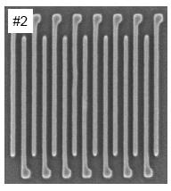
7 Claymore: 32nm Programmed defect layout SRAM M1 All sections (32nm, 40nm, and 48nm) have the same corner marks and unit cell step distances X = 2um, Y = 3um 48nm section 40nm section Pillararray Line / space SRAM M1 Pillar array 32 nm 40nm and 48nm feature types are the same design with different dummy shrinks. 32nm section Line / space SRAM M1 Pillar array 228um Line / space M1 Contact L/S 162um


8 Defect locations Vertical Mouse Bite Horizontal Programmed defects sizes are arrayed every 7 unit cells horizontally Programmed defect types are arrayed every other unit cell vertically Three repeats of each set Separation between PD Sizes 14um Other features types have a similar array of defects 32nm section Line space features Vertical Separation between PD types Extensions 6 m Horizontal Biggest Labeled 12 to 1 Smallest


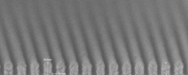
9 Programmed Defects for 32nm Patterns Programmed defects start at 4nm and increase in increments of 4nm up to 48nm M1 4x32nm 32x32nm 32x48nm L/S Contact

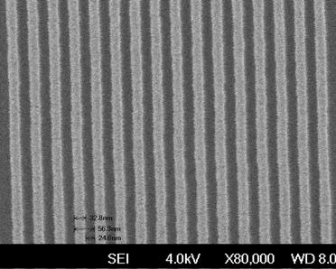
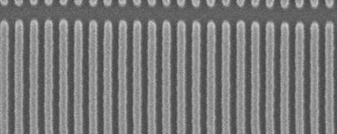
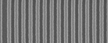
10 Mask and Imprint Analysis SEMs of the Mask were captured with a Holon EMU-270A SEM 1.5 nm resolution at 1.0 kv when applying aberration correction. Low vacuum and charge control enable high quality imaging on fused silica masks. Images of the imprints taken with a JEOL JSM-6340F field emission cold cathode SEM 1.2 nm resolution capability at 15 kv and 2.5nm at 1 kv.


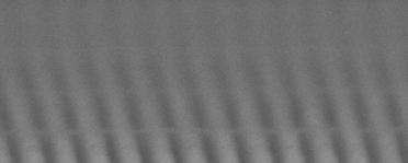
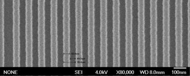
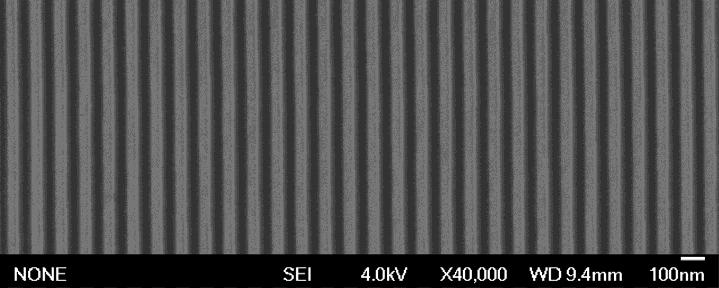
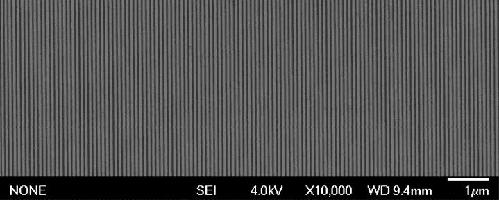
11 32 nm Half Pitch Lines 20nm Mask Imprint


12 PD measured area evaluation process DAFC Defect Analysis for the Financially Challenged Smoothing & Threshold segmentation Image A - Image B Image A Image Shift by pitch Image B Count white pixels and convert to area 2349 nm 2
13 Measured area compared to data size Mid-line extension Shrinking Pillar Measured PD area (nm^2) Measured PD area (nm^2) Imprint Template Data Size (nm^2) Imprint Template Data Size (nm^2)


14 Electron beam inspection systems KLA-Tencor es35 Die-to-die Image contrast inspection Pixel size: 15, 20, 25nm Landing energy 1750V Data rate 50mpps Hermes Microvision escan 315 Die-to-die Image contrast inspection Pixel size: 10, 15nm Landing energy: 2000V Data rate 100mpps NGR 2100 Die-to-database Fast CD inspection Pixel size: 3nm Landing energy 2600V Data rate 50mpps
15 Programmed defect pixel progression Programmed Defects nm (6nm) y-loc (um) Setup errors 40nm (5nm) Big 32nm (4nm) Small x-loc (um) PD_Loc PD_Loc 15nm PD_Loc Pixel 20nm PD_Loc Pixel 25nm Pixel
 100% 80% 60% 40% 20% 0% 32nm Features 15nm Pixel Inspection 1")
 (nm^2) Shrinking Pillar pillar SRAM_mid-line Ext")
16 80% capture rate examples The sensitivity range is 10 to 18nm for an 80% capture rate Capture Probability (%) 100% 80% 60% 40% 20% 0% 32nm Features 15nm Pixel Inspection 1 327nm^2 ~10nm PD nm^2 ~18nm PD Measure Data PD Size area (nm) (nm^2) Shrinking Pillar pillar SRAM_mid-line Ext ext 1 2
17 escan 315: e-beam wafer inspection 32nm HP Metal-1 VM HM VE HE VM HM VE HE VM HM VE HE nm Parameters: 100 MPPS 2000V 3nA Pillar Lines VM HM VE HE VM HM VE HE VM HM VE HE VM HM VE HE VM HM VE HE VM HM VE HE 15nm pixel 10nm pixel
18 Captured Programmed Defects: 10nm Pixel Programmed defects: 8nm 12nm Metal-1 Pillars Lines Mousebite 8nm H Mousebite 8nm H Mousebite 12nm Line Shortening 8nm V Mousebite 8nm V Mousebite 12nm Mid Extension 8nm H Extension 8nm H Extension 12nm Line Extension 8nm V Extension 8nm V Extension 12nm


19 KLA-T 6xx Optical Inspection Results Because the background noise is low, it is possible to discern the defect without resolving the 32nm pattern. The KLA-T 6xx platform works in both Transmitted and Reflected light modes. Transmitted and Reflected Light capture different types of defects. Having both modes essential for capturing critical defects. In these examples, one defect in the 32nm half pitch pattern has signal in transmitted and one in reflected mode. Def #1 Def #2 Inspection of 32nm half pitch patterns Difference Reference PD Cell Transmitted Transmitted Reflected Reflected

20 Modulation vs. Programmed defect size Modulation tracks well with the measured defect size in the mask Sensitivity is on the order of 32nm Thresholds can be optimized to increase sensitivity Measured defect size vs. coded defect size Modulation vs. defect size during 6xx inspection Measured PD area PD (nm^2) area (nm 2 ) Modulation Imprint Template Data Size (nm^2) 2 ) Defect size (nm)


21 Infrastructure: Template Repair RaveLLC Nawotec Nanomachining system E-beam Deposition/Etch


22 Repair Examples After repair on a RaveLLC 650nm system Before repair Quartz Line Quartz defect After AFM repair 300 nm defect 50 nm defect 50 nm trench

23 Zeiss: MeRiT MG E-beam Mask Repair


24 Repairs: After Imprint 40nm 32nm
25 So is this this technology really going to work?


26 Emerging Market Applications J-FIL TM nanopatterning advantages can serve a variety of markets Semiconductor ICs Hard Disk Drives J-FIL s low cost, high resolution patterning enables increase memory capacity at lower cost per bit Drives resolution and cost of ownership for both CMOS and magnetic memory Emerging Applications Displays Solar Batteries Nano-Bio J-FIL enables a broad range of other market opportunities with low cost, high resolution, and large substrate area patterning Efficiency Cost Brightness Efficiency Capacity Faster Recharge Drug Delivery Targeting And Efficacy


 150mm")

27 Full Wafer/Disk Imprint Process Thin Template Imprio 1100 (Photonic Crystals) 150mm Diameter Patterned Media Template Imprio HD7000 (Patterned Media)


28 Hard Drives Hard disk drives operate by storing bits of information on a disk coated with a magnetically influenced film Magnetic media These things have been working for years. What s the problem?
29
30 Why Imprint Lithography for Patterned Media? Let s compare the Information storage roadmap against the well established ITRS Roadmap for integrated circuits Half Pitch nm Next Generation Lithography 193i no resolution EUV $$$, timing for 1Tb EBDW Low throughput UV-IL right combination MPU DRAM Flash Storage Year 1Tb/in 2 The Storage Roadmap is much more aggressive than the ITRS Roadmap High volume optical tools will not be available in time The price of an EUV printing tool is prohibitive (~$50-75M) $90-100M $ M Electron beam writers have the resolution, but not the throughput Imprint offers the best combination of cost, throughput Canon Nanotechnologies, and resolution Inc.


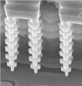
31 High Density Template Fabrication for PM ZEP520 Cr Conventional Method for defining small features E-beam Exposure Cl 2 /O 2 Fluorine based chemistry 6025 Quartz Resist applied to <15 nm of Cr Expose/develop e-beam resist, descum Etch chrome, strip resist Etch quartz, Strip chrome Lift-off Process Alternative methods include: PMMA or ZEP520A lift-off High Resolution HSQ resist Ion beam Lithography Image resist Deposit Cr Lift-off Etch Glass Strip Cr


32 Template Mastering with Rotary E-beam Electron Gun Fabrication of Master Templates for Patterned Media requires high resolution patterning over large areas Sub-50 nm resolution Very low pattern distortion Patterns are concentric lines, arcs, and dot arrays Master template Rotating Spindle Stage Linear Stage Rotational speed: ~ 100 to 3000 rpm Direction: CW or CCW Linear translation in one radial direction


 Quartz")
33 Example: BPM 25nm Half Pitch E-beam write CR Lift-off 25nm half-pitch (250 Gb/in 2 ) Quartz etch Imprint
34 Master Template Fabrication for 1Tb and beyond For Bit Patterned Media (BPM), a 1Tb Master requires a half pitch of nm! While it may be possible to resolve these feature types with a Gaussian beam pattern generator, there are several problems that you will need to overcome Pattern placement of the individual bits and write errors Write time! (7 days at a minimum) An alternative approach is to combine the best attributes of e-beam writing and self assembly Directed Self Assembly


35 Diblock copolymer materials undergo phase separation to form morphologies with short-range order The morphology and phase dimensions are controlled by the chemical composition Processing is simple and cheap, but no long-range order Polymer molecule Uniform film Polymer film Spheres Cylinders Lamellae Canon Inc.


36 Examples: Short-range order From Joy Cheng, IBM Almaden Polymer solution is spincoated on an unpatterned substrate and then annealed for several minutes. PS-b-PMMA Cylinders ~1 micron Uniform feature size and pitch, but no long-range order. (Likely okay for PV applications) Lamellae ~1 micron


37 Directed Self Assembly To achieve long range order, we can use the e-beam writer to guide the placement of the block copolymer Pattern Rectification Density Multiplication Half pitch = 13.5nm

38 Another DSA Example


39 Template Inspection Candela X-Beam Optical Surface Analyzer Multi-channel inspection of optical properties Scattered light dark field Reflected light bright field, reflectometry Phase shift thin film measurements This work: Candela 6120: disk substrates Candela CS20: templates Circumferential Laser Scattered light detector Radial Laser = 408 nm Combination phase and specular detector = 408 nm Polarizer Rotating spindle stage

? How do we track defectivity?")
40 Identifying Defects on Templates and Disks Template Imprint A Imprint B Specular Inspection There are 3 critical defects that need to be tracked: template, particle, non-fill How do we identify each defect type (defect classification)? How do we track defectivity? - From template to disk - From disk to disk

41 Defect Source Analysis Defect Count Total inspected area: ~ 29 cm 2 Total defectivity: ~ 2.4 def/cm 2


42 Liquid Crystal Display Panel Fabrication LCD displays are ubiquitous: LCD Panel Components


43 Nanoscale Patterning Can Improve Many Critical Components in Displays J-FIL TM can offer improved technologies at lower cost that impacts approximately 50% of liquid crystal display Bill of Materials (BoM).
")

44 LithoFlex 350 TM SYSTEM CONFIGURATION LithoFlex 350 Plate-to-Roll (P2R) or Roll-to-Plate (R2P) Template Substrates: P2R < 300mm glass or silicon wafer R2P < 350mm width web Automated or manual template loading Automatic protective film particle control UV cure (365nm) light source PERFORMANCE Sub-50 nanometer feature resolution Throughput >1 meter per minute Position accuracy of 600 microns (3 ) Alignment Option Available Print width: 300mm maximum TECHNOLOGY Jet and Flash TM imprint technology IntelliJet TM resist jetting dispensing system

45 Plate to Roll (P2R) imprinting P2R imprinting uses patterned rigid substrates: As an example, a 300mm wafer can be used as the working template Can be patterned several different ways: - Photolithography - Imprint Lithography - Electron beam Lithography - Photo or E-beam/DSA


46 J-FIL Results Protective film removed 350mm web with protective film Pattern close-up


47 Test Pattern SEM images Both micron size and nanoscale patterns can be imprinted within the same field Micron scale pattern 450nm test pattern


48 Nanoscale imprinting 50nm half pitch grating


49 Wire Grid Polarizers Two methods for fabricating Wire Grid Polarizers(WGPs): Very low cost Al Resist Very High Performance Template Glass Substrate Resist Residual layer Al Imprint Al WGP


50 Etched WGP Results Performance is driven by many factors Defectivity Pitch Duty Cycle Aspect Ratio Al quality Integrated Transmittance : ~44% Extinction ratio at 550nm: ~50K
51 Final Thoughts X-ray Lithography 1X proximity-based technology using a membrane-based mask Ion Beam Lithography 1X and projection technology using a stencil-based mask SCALPEL Projection electron lithography using a thin membrane mask PrXL IBL SCALPEL 1. I worked on all three mask technologies 2. From a manufacturing perspective, all three are now dead 3. All three died, in part, from a lack of mask infrastructure
52 Acknowledgments CNT and Molecular Imprints Ecron Thompson, Gerard Schmid, Mike Miller, Kosta Selinidis, Ian McMackin, Cindy Brooks, Gary Doyle, Gaddi Haase, Kang Luo, Lovejeet Singh, David Curran DNP Shiho Sasaki, Nobuhito Toyama, Masaaki Kurihara, and Naoya Hayashi Motorola Bill Dauksher, Kevin Nordquist, Kathy Gehoski, Ngoc Le, Eric Ainley, Steve Smith KLA-Tencor Mark McCord Vistec-Semiconductor Tim Groves, Mike Butler, Eric Tapley, Olaf Fortagne Photronics, Toppan Photomask, IMS Chips, NGR, LBNL, RaveLLC, Zeiss, NuFlare, Mentor Graphics, HMI This work was partially funded by: DARPA (N C-8011, N ) and NIST-ATP
53 References To learn more about Jet and Flash Imprint Lithography, go to:
54 Appendix Applications Photonic Crystals Contacts Memory Dual Damascene Micro Lens Arrays SAW Devices


55 An Example: Photonic Crystal 80nm HP Example: Photonic Crystal Array Pattern Transfer After Imprint After Planarization After Dry Develop After Cr/Glass etch


56 The Complete S-FIL Process: Contacts Template: 80 nm dense pillars Imprinted Etch Barrier Etched 80 nm contacts


57 Hoya: 30nm IBM Memory Template Imprint Si Etch X-Section Ox Si BOx


58 Dual Damascene metal levels via levels Template by Toppan Replication on Imprio TM 55, Willson et al. at UT.


59 Micro Lens Arrays Background: Added to a digital camera s CMOS/CCD image chip to improve optical collection efficiency Challenge: Patterning of high packing density aspheric lens arrays requiring no etching Template Imprinted Lens Array


60 SAW Device Fabrication Step 1. Create Template Step 2. Imprint, etch the aluminum IDT, and remove the resist Input Output The patterned aluminum (light grey) is 40 nm thick X 130 nm wide, and the substrate material (dark grey) is LiNbO 3. Template Note the line uniformity and the absence of line edge roughness in the final pattern.
Nano-Imprint Lithography Infrastructure: Imprint Templates
 Nano-Imprint Lithography Infrastructure: Imprint Templates John Maltabes Photronics, Inc Austin, TX 1 Questions to keep in mind Imprint template manufacturability Resolution Can you get sub30nm images?
Inspection of 32nm imprinted patterns with an advanced e-beam inspection system
 Inspection of 32nm imprinted patterns with an advanced e-beam inspection system Hong Xiao, Long (Eric) Ma, Fei Wang, Yan Zhao, and Jack Jau Hermes Microvision, Inc., 1762 Automation Parkway, San Jose,
Inspection of Imprint Lithography Patterns for Semiconductor and Patterned Media
 Inspection of Imprint Lithography Patterns for Semiconductor and Patterned Media Douglas J. Resnick, Gaddi Haase, Lovejeet Singh, David Curran, Gerard M. Schmid, Kang Luo, Cindy Brooks, Kosta Selinidis,
PROGRESS OF UV-NIL TEMPLATE MAKING
 PROGRESS OF UV-NIL TEMPLATE MAKING Takaaki Hiraka, Jun Mizuochi, Yuko Nakanishi, Satoshi Yusa, Shiho Sasaki, Yasutaka Morikawa, Hiroshi Mohri, and Naoya Hayashi Electronic Device Laboratory, Dai Nippon
UV Nanoimprint Tool and Process Technology. S.V. Sreenivasan December 13 th, 2007
 UV Nanoimprint Tool and Process Technology S.V. Sreenivasan December 13 th, 2007 Agenda Introduction Need tool and process technology that can address: Patterning and CD control Alignment and Overlay Defect
Defect Reduction for Semiconductor Memory Applications Using Jet And Flash Imprint Lithography
 Defect Reduction for Semiconductor Memory Applications Using Jet And Flash Imprint Lithography Zhengmao Ye, Kang Luo, Xiaoming Lu, Brian Fletcher, Weijun Liu, Frank Xu, Dwayne LaBrake, Douglas Resnick,
The Transition to Patterned Media in Hard Disk Drives
 The Transition to Patterned Media in Hard Disk Drives The Evolution of Jet and Flash Imprint Lithography for Patterned Media DISKCON San Jose Sept 24 rd, 2009 Paul Hofemann, Vice President, HDD Future
The Challenges in Making NIL Master Templates
 The Challenges in Making NIL Master Templates Naoya Hayashi Dai Nippon Printing Co., Ltd. A Member of the ebeam Initiative 2011 Dai Nippon Printing Co.,Ltd. All Rights Reserved. OUTLINE Recent Progress
Fabrication of Step and Flash TM Imprint Lithography Templates Using Commercial Mask Processes
 Fabrication of Step and Flash TM Imprint Lithography Templates Using Commercial Mask Processes Ecron Thompson, Peter Rhyins, Ron Voisin, S.V. Sreenivasan *, Patrick Martin Molecular Imprints, Inc., 1807C
Controlling Linewidth Roughness in Step and Flash Imprint Lithography
 Controlling Linewidth Roughness in Step and Flash Imprint Lithography Gerard M. Schmid a, Niyaz Khusnatdinov a, Cynthia B. Brooks a, Dwayne LaBrake a, Ecron Thompson a, Douglas J. Resnick a *, Jordan Owens
Advances in Roll-to-Roll Imprint Lithography for Display Applications Using Self Aligned Imprint Lithography. John G Maltabes HP Labs
 Advances in Roll-to-Roll Imprint Lithography for Display Applications Using Self Aligned Imprint Lithography John G Maltabes HP Labs Outline Introduction Roll to Roll Challenges and Benefits HP Labs Roll
Readiness and Challenges of EUV Mask
 Panel Discussion: EUVL HVM Insertion and Scaling Readiness and Challenges of EUV Mask Takashi Kamo Toshiba Corporation Semiconductor & Storage Products Company Contents [1] Introduction [2] EUV Mask Defect
Flexible Electronics Production Deployment on FPD Standards: Plastic Displays & Integrated Circuits. Stanislav Loboda R&D engineer
 Flexible Electronics Production Deployment on FPD Standards: Plastic Displays & Integrated Circuits Stanislav Loboda R&D engineer The world-first small-volume contract manufacturing for plastic TFT-arrays
Self-Aligned Double Patterning for 3xnm Flash Production
 Self-Aligned Double Patterning for 3xnm Flash Production Chris Ngai Dir of Process Engineering & Lithography Maydan Technology Center Group Applied Materials, Inc. July 16 th, 2008 Overview Double Patterning
Abstract. Keywords INTRODUCTION. Electron beam has been increasingly used for defect inspection in IC chip
 Abstract Based on failure analysis data the estimated failure mechanism in capacitor like device structures was simulated on wafer in Front End of Line. In the study the optimal process step for electron
Recent results of Multi-beam mask writer MBM-1000
 Recent results of Multi-beam mask writer MBM-1000 Hiroshi Matsumoto, Hiroshi Yamashita, Hideo Inoue, Kenji Ohtoshi, Hirokazu Yamada Member of the ebeam Initiative 1 NFT s mask writer roadmap 2016 Device
New Worlds for Polymers: Organic Transistors, Light Emitting Diodes, and Optical Waveguides Ed Chandross
 New Worlds for Polymers: Organic Transistors, Light Emitting Diodes, and Optical Waveguides Ed Chandross Materials Chemistry, LLC 1 Polymers in the Electronic Industry Enabling Materials Active Materials?
Semiconductors Displays Semiconductor Manufacturing and Inspection Equipment Scientific Instruments
 Semiconductors Displays Semiconductor Manufacturing and Inspection Equipment Scientific Instruments Electronics 110-nm CMOS ASIC HDL4P Series with High-speed I/O Interfaces Hitachi has released the high-performance
Approaching Zero Etch Bias at Cr Etch Process
 Approaching Zero Etch Bias at Cr Etch Process Pavel Nesladek a ; Norbert Falk b ; Andreas Wiswesser a ; Renee Koch b ; Björn Sass a a Advanced Mask Technology Center, Rähnitzer Allee 9; 01109 Dresden,
Advanced Display Manufacturing Technology
 Advanced Display Manufacturing Technology John Busch Vice President, New Business Development Display and Flexible Technology Group September 28, 2017 Safe Harbor This presentation contains forward-looking
Photomask BACUS The international technical group of SPIE dedicated to the advancement of photomask technology.
 Photomask BACUS The international technical group of SPIE dedicated to the advancement of photomask technology. June 2011 Volume 27, Issue 6 Paper 7970-8 Progress in Mask Replication using Jet and Flash
Auto classification and simulation of mask defects using SEM and CAD images
 Auto classification and simulation of mask defects using SEM and CAD images Tung Yaw Kang, Hsin Chang Lee Taiwan Semiconductor Manufacturing Company, Ltd. 25, Li Hsin Road, Hsinchu Science Park, Hsinchu
Wafer defects can t hide from
 WAFER DEFECTS Article published in Issue 3 2016 Wafer defects can t hide from Park Systems Atomic Force Microscopy (AFM) leader Park Systems has simplified 300mm silicon wafer defect review by automating
Parts of dicing machines for scribing or scoring semiconductor wafers , , , , ,
 US-Rev3 26 March 1997 With respect to any product described in or for Attachment B to the Annex to the Ministerial Declaration on Trade in Information Technology Products (WT/MIN(96)/16), to the extent
Lossless Compression Algorithms for Direct- Write Lithography Systems
 Lossless Compression Algorithms for Direct- Write Lithography Systems Hsin-I Liu Video and Image Processing Lab Department of Electrical Engineering and Computer Science University of California at Berkeley
SEMICONDUCTOR TECHNOLOGY -CMOS-
 SEMICONDUCTOR TECHNOLOGY -CMOS- Fire Tom Wada What is semiconductor and LSIs Huge number of transistors can be integrated in a small Si chip. The size of the chip is roughly the size of nails. Currently,
Electron Beam Technology
 Electron Beam Technology Speed up! High Performance Electron Beam Lithography dedicated electron beam lithography To bridge cutting-edge research and nanofabrication, a dedicated nanolithography solution
Characterization and improvement of unpatterned wafer defect review on SEMs
 Characterization and improvement of unpatterned wafer defect review on SEMs Alan S. Parkes *, Zane Marek ** JEOL USA, Inc. 11 Dearborn Road, Peabody, MA 01960 ABSTRACT Defect Scatter Analysis (DSA) provides
SEMICONDUCTOR TECHNOLOGY -CMOS-
 SEMICONDUCTOR TECHNOLOGY -CMOS- Fire Tom Wada 2011/12/19 1 What is semiconductor and LSIs Huge number of transistors can be integrated in a small Si chip. The size of the chip is roughly the size of nails.
Introduction and recent results of Multi-beam mask writer MBM-1000
 Introduction and recent results of Multi-beam mask writer MBM-1000 Hiroshi Matsumoto, Yasuo Kato, Munehiro Ogasawara, Hirokazu Yamada February 23 rd, 2016 Member of the ebeam Initiative NFT s mask writer
1. Publishable summary
 1. Publishable summary 1.1. Project objectives. The target of the project is to develop a highly reliable high brightness conformable low cost scalable display for demanding applications such as their
Wafer Thinning and Thru-Silicon Vias
 Wafer Thinning and Thru-Silicon Vias The Path to Wafer Level Packaging jreche@trusi.com Summary A new dry etching technology Atmospheric Downstream Plasma (ADP) Etch Applications to Packaging Wafer Thinning
Development of OLED Lighting Applications Using Phosphorescent Emission System
 Development of OLED Lighting Applications Using Phosphorescent Emission System Kazuhiro Oikawa R&D Department OLED Lighting Business Center KONICA MINOLTA ADVANCED LAYERS, INC. October 10, 2012 Outline
Multi-Shaped E-Beam Technology for Mask Writing
 Multi-Shaped E-Beam Technology for Mask Writing Juergen Gramss a, Arnd Stoeckel a, Ulf Weidenmueller a, Hans-Joachim Doering a, Martin Bloecker b, Martin Sczyrba b, Michael Finken b, Timo Wandel b, Detlef
Screen investigations for low energetic electron beams at PITZ
 1 Screen investigations for low energetic electron beams at PITZ S. Rimjaem, J. Bähr, H.J. Grabosch, M. Groß Contents Review of PITZ setup Screens and beam profile monitors at PITZ Test results Summary
The hybrid photon detectors for the LHCb-RICH counters
 7 th International Conference on Advanced Technology and Particle Physics The hybrid photon detectors for the LHCb-RICH counters Maria Girone, CERN and Imperial College on behalf of the LHCb-RICH group
IN-VISION All rights reserved. IN-VISION GmbH. B2B DLP Light Engine and Optical Solutions
 IN-VISION 2017. All rights reserved. IN-VISION GmbH B2B DLP Light Engine and Optical Solutions Company Long-term experience in development and manufacturing of high-end optical projection lens assemblies
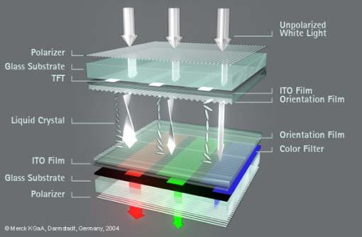
Liquid Crystal Display (LCD)
") Liquid Crystal Display (LCD) When coming into contact with grooved surface in a fixed direction, liquid crystal molecules line up parallelly along the grooves. When coming into contact with grooved surface
Liquid Crystal Display (LCD) When coming into contact with grooved surface in a fixed direction, liquid crystal molecules line up parallelly along the grooves. When coming into contact with grooved surface
EUV Mask and Wafer Defectivity: Strategy and Evaluation for Full Die Defect Inspection
 EUV Mask and Wafer Defectivity: Strategy and Evaluation for Full Die Defect Inspection Ravi Bonam 1, Hung-Yu Tien 2, Acer Chou 2, Luciana Meli 1, Scott Halle 1, Ivy Wu 2, Xiaoxia Huang 2, Chris Lei 2,
Advancements in Acoustic Micro-Imaging Tuesday October 11th, 2016
 Central Texas Electronics Association Advancements in Acoustic Micro-Imaging Tuesday October 11th, 2016 A review of the latest advancements in Acoustic Micro-Imaging for the non-destructive inspection
SPATIAL LIGHT MODULATORS
 SPATIAL LIGHT MODULATORS Reflective XY Series Phase and Amplitude 512x512 A spatial light modulator (SLM) is an electrically programmable device that modulates light according to a fixed spatial (pixel)
INSTRUMENT CATHODE-RAY TUBE
 INSTRUMENT CATHODE-RAY TUBE 14 cm diagonal rectangular flat face domed mesh post-deflection acceleration improved spot quality for character readout high precision by internal permanent magnetic correction
AMOLED Manufacturing Process Report SAMPLE
 AMOLED Manufacturing Process Report SAMPLE 2018 AMOLED Manufacturing Process Report The report analyzes the structure and manufacturing process by dividing AMOLED into small & medium-sized rigid OLED,
Supplementary Figure 1. OLEDs/polymer thin film before and after peeled off from silicon substrate. (a) OLEDs/polymer film fabricated on the Si
 OLEDs/polymer film fabricated on the Si") Supplementary Figure 1. OLEDs/polymer thin film before and after peeled off from silicon substrate. (a) OLEDs/polymer film fabricated on the Si substrate. (b) Free-standing OLEDs/polymer film peeled off
Supplementary Figure 1. OLEDs/polymer thin film before and after peeled off from silicon substrate. (a) OLEDs/polymer film fabricated on the Si substrate. (b) Free-standing OLEDs/polymer film peeled off
LEP400 Etch Depth Monitor Real-time, in-situ plasma etch depth monitoring and end point control plus co-linear wafer vision system
 LEP400 Etch Depth Monitor Real-time, in-situ plasma etch depth monitoring and end point control plus co-linear wafer vision system Base Configuration Etch Depth Monitoring LEP400 Recessed Window Plasma
Content. Core Technology (Short introduction) LCMO (Light Controlled Molecular Orientation) technology
 LCMO (Light Controlled Molecular Orientation) technology") Content Core Technology (Short introduction) LCMO (Light Controlled Molecular Orientation) technology LCMO Patterned Films for Light management : Applications Examples LCMO- Photo Patterned Retarders LCMO-
Content Core Technology (Short introduction) LCMO (Light Controlled Molecular Orientation) technology LCMO Patterned Films for Light management : Applications Examples LCMO- Photo Patterned Retarders LCMO-
PROCESS TECHNOLOGIES FOR ADVANCED ORGANIC ELECTRONIC DEVICES: MICRODISPLAYS, LIGHTING AND SOLAR CELLS
 PROCESS TECHNOLOGIES FOR ADVANCED ORGANIC ELECTRONIC DEVICES: MICRODISPLAYS, LIGHTING AND SOLAR CELLS Dr. Christian May Fraunhofer IPMS - Center for Organic Materials and Electronic Devices Dresden COMEDD
projectors, head mounted displays in virtual or augmented reality use, electronic viewfinders
 Beatrice Beyer Figure 1. (OLED) microdisplay with a screen diagonal of 16 mm. Figure 2. CMOS cross section with OLED on top. Usually as small as fingernails, but of very high resolution Optical system
ABSTRACT. Keywords: 3D NAND, FLASH memory, Channel hole, Yield enhancement, Defect inspection, Defect reduction DISCUSSION
 Yield enhancement of 3D flash devices through broadband brightfield inspection of the channel hole process module Jung-Youl Lee a, Il-Seok Seo a, Seong-Min Ma a, Hyeon-Soo Kim a, Jin-Woong Kim a DoOh Kim
Spatial Light Modulators XY Series
 Spatial Light Modulators XY Series Phase and Amplitude 512x512 and 256x256 A spatial light modulator (SLM) is an electrically programmable device that modulates light according to a fixed spatial (pixel)
Sep 09, APPLICATION NOTE 1193 Electronic Displays Comparison
 Sep 09, 2002 APPLICATION NOTE 1193 Electronic s Comparison Abstract: This note compares advantages and disadvantages of Cathode Ray Tubes, Electro-Luminescent, Flip- Dot, Incandescent Light Bulbs, Liquid
Methodology for Trench Capacitor Etch Optimization using Voltage Contrast Inspection and Special Processing
 Methodology for Trench Capacitor Etch Optimization using Voltage Contrast Inspection and Special Processing 1 Oliver D. Patterson, 1 Xing J. Zhou, 1 Rohit S. Takalkar, 1 Katherine V. Hawkins, 1 Eric H.
These are used for producing a narrow and sharply focus beam of electrons.
 CATHOD RAY TUBE (CRT) A CRT is an electronic tube designed to display electrical data. The basic CRT consists of four major components. 1. Electron Gun 2. Focussing & Accelerating Anodes 3. Horizontal
MTI-2100 FOTONIC SENSOR. High resolution, non-contact. measurement of vibration. and displacement
 A worldwide leader in precision measurement solutions MTI-2100 FOTONIC SENSOR High resolution, non-contact measurement of vibration and displacement MTI-2100 Fotonic TM Sensor Unmatched Resolution and
An Overview of the Performance Envelope of Digital Micromirror Device (DMD) Based Projection Display Systems
 Based Projection Display Systems") An Overview of the Performance Envelope of Digital Micromirror Device (DMD) Based Projection Display Systems Dr. Jeffrey B. Sampsell Texas Instruments Digital projection display systems based on the DMD
An Overview of the Performance Envelope of Digital Micromirror Device (DMD) Based Projection Display Systems Dr. Jeffrey B. Sampsell Texas Instruments Digital projection display systems based on the DMD
DIRECT DRIVE ROTARY TABLES SRT SERIES
 DIRECT DRIVE ROTARY TABLES SRT SERIES Key features: Direct drive Large center aperture Brushless motor design Precision bearing system Integrated position feedback Built-in thermal sensors ServoRing rotary
Display Technologies CMSC 435. Slides based on Dr. Luebke s slides
 Display Technologies CMSC 435 Slides based on Dr. Luebke s slides Recap: Transforms Basic 2D Transforms: Scaling, Shearing, Rotation, Reflection, Composition of 2D Transforms Basic 3D Transforms: Rotation,
Lecture Flat Panel Display Devices
 Lecture 1 6.976 Flat Panel Display Devices Outline Overview of 6.976 Overview Flat Panel Display Devices Course website http://hackman.mit.edu Reading Assignment: Article by Alt and Noda, IBM Journal of
Automation in Semiconductor Manufacturing IEDM, San Francisco, 1982 Keynote Speech
 Automation in Semiconductor Manufacturing IEDM, San Francisco, 1982 Keynote Speech Commentary Alongside ISSCC, IEDM is the most traditional academic conference in the semiconductor field, and it is held
Development of Ultra-High-Density (UHD) Silicon Photomultipliers with improved Detection Efficiency
 Silicon Photomultipliers with improved Detection Efficiency") Development of Ultra-High-Density (UHD) Silicon Photomultipliers with improved Detection Efficiency Fabio Acerbi, Alberto Gola, Giovanni Paternoster, Claudio Piemonte, Nicola Zorzi http://iris.fbk.eu/silicon-photomultipliers
Development of Ultra-High-Density (UHD) Silicon Photomultipliers with improved Detection Efficiency Fabio Acerbi, Alberto Gola, Giovanni Paternoster, Claudio Piemonte, Nicola Zorzi http://iris.fbk.eu/silicon-photomultipliers
The Silicon Pixel Detector (SPD) for the ALICE Experiment
 for the ALICE Experiment") The Silicon Pixel Detector (SPD) for the ALICE Experiment V. Manzari/INFN Bari, Italy for the SPD Project in the ALICE Experiment INFN and Università Bari, Comenius University Bratislava, INFN and Università
The Silicon Pixel Detector (SPD) for the ALICE Experiment V. Manzari/INFN Bari, Italy for the SPD Project in the ALICE Experiment INFN and Università Bari, Comenius University Bratislava, INFN and Università
Screens; media that use additive primaries
 Image display Display is the final stage in the image processing pipeline: Continuous scenes are acquired and digitally processed. The display process essentially converts the discrete image back to continuous
Advanced WLP Platform for High-Performance MEMS. Presented by Dean Spicer, Director of Engineering
 Advanced WLP Platform for High-Performance MEMS Presented by Dean Spicer, Director of Engineering 1 May 11 th, 2016 1 Outline 1. Application Drivers for High Performance MEMS Sensors 2. Approaches to Achieving
Joint Development of Ultra-Bright, Inorganic EL Light-Emitting Materials. November 2, 2005 KURARAY CO., LTD.
 Joint Development of Ultra-Bright, Inorganic EL Light-Emitting Materials November 2, 2005 KURARAY CO., LTD. Sales Trends of Display-related Products (Kuraray (standalone)) FY1994 FY1999 FY2004 Sales Ratio
L14 - Video. L14: Spring 2005 Introductory Digital Systems Laboratory
 L14 - Video Slides 2-10 courtesy of Tayo Akinwande Take the graduate course, 6.973 consult Prof. Akinwande Some modifications of these slides by D. E. Troxel 1 How Do Displays Work? Electronic display
High ResolutionCross Strip Anodes for Photon Counting detectors
 High ResolutionCross Strip Anodes for Photon Counting detectors Oswald H.W. Siegmund, Anton S. Tremsin, Robert Abiad, J. Hull and John V. Vallerga Space Sciences Laboratory University of California Berkeley,
HC9000D. Color : Midnight Black
 HOME CINEMA HC9000D NUEVO HC9000D 2 HC9000D - Videoproyector 0,61" 3-SXRD (16:9 Panorámico) - Resolución Full HD 1920x1080 con visión 3D - Luminosidad 1100 ANSI Lumens - Contraste 150.000:1 - Ratio de
Phosphorescent OLED Technologies: The Next Wave. Plastic Electronics Conference Oct 9, 2012
 Phosphorescent OLED Technologies: The Next Wave Plastic Electronics Conference Oct 9, 2012 UDC Company Focus IP innovator, technology developer, patent licensor and materials supplier for the rapidly growing
AIXTRON in EXCILIGHT project
 AIXTRON SE AIXTRON in EXCILIGHT project Gintautas Simkus ABOUT AIXTRON 2 Who we are Headquarter based in Herzogenrath, Germany Worldwide presence with 14 sales/representatives offices and production facilities
Display Technologies. Corning: The Technology Behind the Glass
 Display Technologies Corning: The Technology Behind the Glass Dr. David Chen Director, Application Engineering and Asia Commercial Technology Taiwan Corning Display Technologies Taiwan June 13, 2008 Forward
An Overview of OLED Display Technology
 page:1 An Overview of OLED Display Technology Homer Antoniadis OSRAM Opto Semiconductors Inc. San Jose, CA page:2 Outline! OLED device structure and operation! OLED materials (polymers and small molecules)!
Overcoming Challenges in 3D NAND Volume Manufacturing
 Overcoming Challenges in 3D NAND Volume Manufacturing Thorsten Lill Vice President, Etch Emerging Technologies and Systems Flash Memory Summit 2017, Santa Clara 2017 Lam Research Corp. Flash Memory Summit
2.2. VIDEO DISPLAY DEVICES
 Introduction to Computer Graphics (CS602) Lecture 02 Graphics Systems 2.1. Introduction of Graphics Systems With the massive development in the field of computer graphics a broad range of graphics hardware
INSTRUMENT CATHODE-RAY TUBE
 Instrument cathode-ray tube D14-363GY/123 INSTRUMENT CATHODE-RAY TUBE mono accelerator 14 cm diagonal rectangular flat face internal graticule low power quick heating cathode high brightness, long-life
Technology White Paper Plasma Displays. NEC Technologies Visual Systems Division
 Technology White Paper Plasma Displays NEC Technologies Visual Systems Division May 1998 1 What is a Color Plasma Display Panel? The term Plasma refers to a flat panel display technology that utilizes
High-resolution screens have become a mainstay on modern smartphones. Initial. Displays 3.1 LCD
 3 Displays Figure 3.1. The University of Texas at Austin s Stallion Tiled Display, made up of 75 Dell 3007WPF LCDs with a total resolution of 307 megapixels (38400 8000 pixels) High-resolution screens
Display Systems. Viewing Images Rochester Institute of Technology
 Display Systems Viewing Images 1999 Rochester Institute of Technology In This Section... We will explore how display systems work. Cathode Ray Tube Television Computer Monitor Flat Panel Display Liquid
Scanner PERENITY 5K The best complete scanning solution for Archives
 V-I Technical characteristics HIGHLIGHTS Multi format: 35/S35-16/S16-8/S8, 28-17.5-9.5 5K / 4K / 2K / HD Sprocketless laser detection Picture stabilization through the perforation analysis High-power LED
CNT FIELD EMISSION CATHODE CATALOG. XinRay Systems Inc. April 2014
 CNT FIELD EMISSION CATHODE CATALOG April 2014 Version 1 1 TABLE OF CONTENTS: 1. ABBREVIATIONS... 2 2. INTRODUCTION... 3 3. PRODUCT AT A GLANCE... 6 4. CARBON NANOTUBE (CNT) CATHODE INFORMATION CHART*...
FLEX2017 June, Monterey, USA Dr Mike Cowin, CMO, SmartKem.
 FLEX2017 June, Monterey, USA Dr Mike Cowin, CMO, SmartKem. FLEX2017 June, Monterey, USA Dr Mike Cowin, CMO, SmartKem. EU H2020 FLEXTRANs Grant Objectives A 24 month project (started September 2016) (Grant
Because Innovation Matters
 Because Innovation Matters Silicon Systems Group Toru Watanabe President, Applied Materials, Japan Semicon Japan November 30, 2010 Safe Harbor This presentation contains forward-looking statements, including
Connection for filtered air
 BeamWatch Non-contact, Focus Spot Size and Position monitor for high power YAG, Diode and Fiber lasers Instantly measure focus spot size Dynamically measure focal plane location during start-up From 1kW
New Rotary Magnetron Magnet Bar Improves Target Utilization and Deposition Uniformity
 Society of Vacuum Coaters 2013 Technical Conference Presentation New Rotary Magnetron Magnet Bar Improves Target Utilization and Deposition Uniformity John Madocks & Phong Ngo, General Plasma Inc., 546
Pressure sensor. Surface Micromachining. Residual stress gradients. Class of clean rooms. Clean Room. Surface micromachining
 Pressure sensor Surface Micromachining Deposit sacrificial layer Si PSG By HF Poly by XeF2 Pattern anchors Deposit/pattern structural layer Etch sacrificial layer Surface micromachining Structure sacrificial
CMPE 466 COMPUTER GRAPHICS
 1 CMPE 466 COMPUTER GRAPHICS Chapter 2 Computer Graphics Hardware Instructor: D. Arifler Material based on - Computer Graphics with OpenGL, Fourth Edition by Donald Hearn, M. Pauline Baker, and Warren
Innovative Rotary Encoders Deliver Durability and Precision without Tradeoffs. By: Jeff Smoot, CUI Inc
 Innovative Rotary Encoders Deliver Durability and Precision without Tradeoffs By: Jeff Smoot, CUI Inc Rotary encoders provide critical information about the position of motor shafts and thus also their
LCD MODULE SPECIFICATION
 TECHNOLOGY CO., LTD. LCD MODULE SPECIFICATION Model : MI0220IT-1 Revision Engineering Date Our Reference DOCUMENT REVISION HISTORY DOCUMENT REVISION DATE DESCRIPTION FROM TO A 2008.03.10 First Release.
Digital Light Processing
 A Seminar report On Digital Light Processing Submitted in partial fulfillment of the requirement for the award of degree of Bachelor of Technology in Computer Science SUBMITTED TO: www.studymafia.org SUBMITTED
Mono STN Display Module
 Mono STN Display Module Product Specification Part No. YMS-12864-15CFCBDGL 128 x 64 STN Blue mode Display For more information, please visit www.andersdx.com or email info@andersdx.com Version 1.0 S FOR
Next Generation of Poly-Si TFT Technology: Material Improvements and Novel Device Architectures for System-On-Panel (SOP)
") Next Generation of Poly-Si TFT Technology: Material Improvements and Novel Device Architectures for System-On-Panel (SOP) Tolis Voutsas* Paul Schuele* Bert Crowder* Pooran Joshi* Robert Sposili* Hidayat
Next Generation of Poly-Si TFT Technology: Material Improvements and Novel Device Architectures for System-On-Panel (SOP) Tolis Voutsas* Paul Schuele* Bert Crowder* Pooran Joshi* Robert Sposili* Hidayat
Cathode Studies at FLASH: CW and Pulsed QE measurements
 Cathode Studies at FLASH: CW and Pulsed QE measurements L. Monaco, D. Sertore, P. Michelato S. Lederer, S. Schreiber Work supported by the European Community (contract number RII3-CT-2004-506008) 1/27
ABSTRACT 1 INTRODUCTION
 Novel lithography technique using an ASML Stepper/Scanner for the manufacture of display devices in MEMS world ASML US, Inc Special Applications, 6580 Via Del Oro San Jose, CA 95119 Keith Best, Pankaj
24. Scaling, Economics, SOI Technology
 24. Scaling, Economics, SOI Technology Jacob Abraham Department of Electrical and Computer Engineering The University of Texas at Austin VLSI Design Fall 2017 December 4, 2017 ECE Department, University
Micro-machining of transparent materials with. nano, pico and femtosecond lasers
 Micro-machining of transparent materials with nano, pico and femtosecond lasers - a review M.R.H. Knowles Oxford Lasers Ltd., Unit 8, Moorbrook Park, Didcot, Oxon OX11 7HP. 1. Motivation Applications &
EE C247B ME C218 Introduction to MEMS Design Spring 2017
 EE C247B ME C218 Introduction to MEMS Design Spring 2017 Prof. Clark T.-C. Nguyen Dept. of Electrical Engineering & Computer Sciences University of California at Berkeley Berkeley, CA 94720 Lecture Module
PTIK UNNES. Lecture 02. Conceptual Model for Computer Graphics and Graphics Hardware Issues
 E3024031 KOMPUTER GRAFIK E3024032 PRAKTIK KOMPUTER GRAFIK PTIK UNNES Lecture 02 Conceptual Model for Computer Graphics and Graphics Hardware Issues 2014 Learning Objectives After carefully listening this
EUV Blank Inspection
 EUV Blank Inspection J.H. Peters* a, C. Tonk a, D. Spriegel b, Hak-Seung Han c, Wonil Cho c, Stefan Wurm d a Advanced Mask Technology Center, Raehnitzer Allee 9, 01109 Dresden, Germany; b Siemens AG, Corporate
EQUIPMENT COATING SYSTEMS FOR THIN-FILM PV THIN-FILM PHOTOVOLTAICS. SCALA VISS PIA nova GC120VCR XENIA
 THIN-FILM PHOTOVOLTAICS EQUIPMENT COATING SYSTEMS FOR THIN-FILM PV SCALA VISS PIA nova GC120VCR XENIA OUR STORY. OUR EXPERIENCE. RANGE OF APPLICATIONS VON ARDENNE provides advanced PVD coating equipment
Layout Analysis Analog Block
 Layout Analysis Analog Block Sample Report Analysis from an HD Video/Audio SoC For any additional technical needs concerning semiconductor and electronics technology, please call Sales at Chipworks. 3685
An Alternative Architecture for High Performance Display R. W. Corrigan, B. R. Lang, D.A. LeHoty, P.A. Alioshin Silicon Light Machines, Sunnyvale, CA
 R. W. Corrigan, B. R. Lang, D.A. LeHoty, P.A. Alioshin Silicon Light Machines, Sunnyvale, CA Abstract The Grating Light Valve (GLV ) technology is being used in an innovative system architecture to create