Elwin Cabrera May 11, 2016 DIGITAL CLOCK. ECE271/CSC222 Final Project Report
|
|
|
- Ashlyn Hodge
- 5 years ago
- Views:
Transcription

1 Elwin Cabrera May 11, 2016 DIGITAL CLOCK ECE271/CSC222 Final Project Report

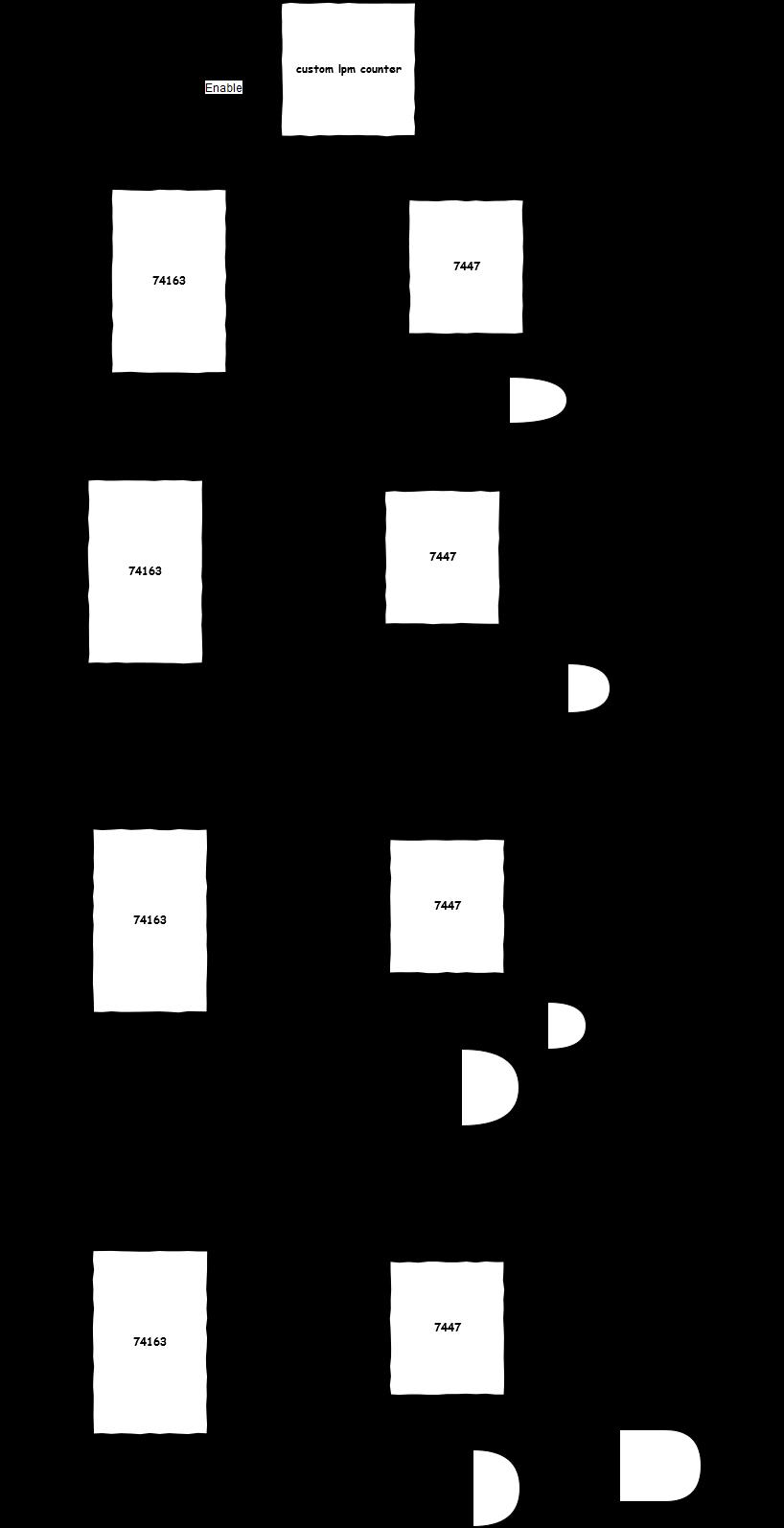
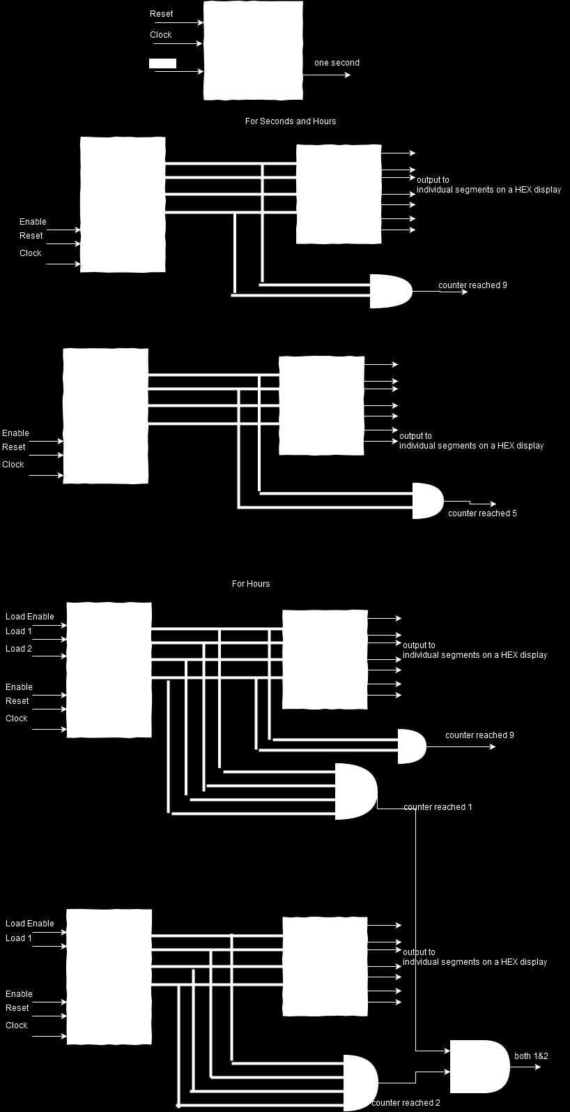
2 Problem Specification: For our CSC222/ECE271 final, we had to design a digital clock. We had to use Quartus and design a control unit and data unit using a block schematic. We had to get to the clock to work like a normal clock counting the hours, minutes, and seconds, as well as keep tracking of AM/PM. We also had to encode a reset into the clock which would reset the clock to 12:00.00 after pressing a key. Requirement Specification: We used Quartus as our program holding all our information and what we worked on inside of it. To test our program we would run it in Quartus, then plug in our FPGA's to see if the clock would visibly run correctly. To program the clock we used a number of different operations. In our data unit, we used: one big LPM counter, six counters, seven 7447 BCD to 7 segment decoders, one toggle flip flop, and glue logic using an, or, and not gates. In our control unit, we used: nine states, transitions between every state, and inputs and outputs for every state. Design Spec: I. Data unit: For the Data Unit we used one custom counter that was an up counter, with a modulus count of 49,999,999. We did this because our clock is 50Mhz and it takes 50,000,000 clock cycles for a second to pass and we want to know when exactly it reached one second not when one second has passed so we took away one clock cycle to the modulus. The custom counter we made has inputs reset, enable, and clock and only one output. The enable input of our custom counter is used for enabling the counter to start counting, and our reset input of the counter is used to tell the counter to reset itself and start counting again and the output of the counter just tells us when it s a second (it goes high every second). Both inputs of our custom counter is then fed to an output of our control unit so the control unit can tell when the counter should be enabled or reset. In addition to a custom counter we also used some other counter components found in the Quartus software (the counter). For each of the seconds and the minute s section we had these counters having only three inputs and for outputs. The inputs were the enable, clock, and the reset which was an active low so we had to not them in order to make them function how we want it. The enable is for enabling the counter and telling it if we want it to start counting and the reset is for resetting the counter to start counting again from one clock cycle again and all of the counters including the custom counter were connected by the same clock. Both these inputs were fed to the outputs of our control unit so we can manage the enables and resets of the counter individual counters. The four outputs for each counter are connected to a binary coded decimal to seven segment display decoder that displays what binary number the counter is outputting in to the decoder. We used a total of


3 six of these counters and six of the decoders two for the seconds two for the minutes and two for the hours. We used a binary coded decimal to seven segment display decoder (7447 decoder in Quartus). The decoder takes four inputs and takes in binary values and displays it in decimal format, we have these outputs going to each segment of a HEX display on the Altera board we tested our design in. we also decided to make one of the HEX to always display a dash line. For the AM and PM we used a toggle flip flop. This flip flop had only three inputs and one output. The inputs were the enable, clear, and the clock. The enable enables the output which was outputted to a single segment in a HEX display so it can switch from A to P, and the reset is to reset back to its original state which is A. Because we only need to enable one HEX for the display to switch from A to P we also had to disable the bottom HEX to always be off. We put this all these components together to make our data path, we also made separate outputs with glue logic to indicate when the outputs were supposed to reset. For example we had the outputs from our connected to a two input and gate telling the system that its nine seconds and the same thing for 50seconds we did this for both our minutes and our seconds so we can send that signal to our control unit so the counter to be reset. However, our hours were different since a regular 12hour format clock resets after 12 back to one, we had to use glue logic with a four input and gate indicating when it was an individual counter reached 2 and the same thing for when it reached 1. Also, since we wanted our clock to reset after 12 we loaded in binary bits of 1 to one counter and 1 and 2 another so we can specify in our control unit that we want those values loaded in when it s past 12 and then reset every counter except the counter. Each output of our control unit is connected to an input to our data path and every output of our data path is connected to an input of our control unit, we had this
4 implementation because we wanted the control unit to have control over when to reset and enable the clock. Below is a picture of our data path implementation: (NOTE: all of these components are connected by one clock)
5

6 II. Control unit: Our initial state for our control unit is our reset state. When we flip the switch, it turns the clock on to start counting. If we turn the switch off then back on, it resets everything, and enables the clock to load in 12 and reset to AM. The reset transitions to the counting state when the switch is turned on, and no equal to a count of one second. Boolean for our reset state: The counting state works with the LPM counter, enabling the clock to start counting. It also controls everything, telling the program where, when, and under what circumstances to transition. The counting state can transition to any state, except returning to the reset, which takes precedence. The first state counting transitions to is Secs09. Secs09 is the ones place for seconds. The output for counting to go to Secs09, is when the counter is equal to one second, but not equal to ten. When in this state, it enables second_one, the ones place for seconds, to count up and resets the count. After one clock cycle, it transitions back to counting. Boolean for our Sces09 state: Secs50 is the tens place for seconds. The output required to transition here is when the count is equal to nine seconds in the one place and one second resulting in ten seconds. Here, the ones place for seconds is reset back to zero, as well as the count, and it enables second_tens, the tens place for seconds, to count up one. After one clock cycle, it transitions back to counting. Boolean for Secs 50 state: Mins09 is the ones place for minutes. The output for counting to go to Mins09 is when the clock is equal to fifty seconds, nine seconds, and a count of one second, but not equal to ten minutes. In this state, both the ones and tens place for seconds are reset, as well as the count. In this state it enables the minutes_one, the ones places for minutes, to count up one. After one clock cycle, it transitions back to
7 counting. Boolean for Mins09 state: The next state counting transitions to is Mins50. It transitions when the clock is equal to nine minutes, fifty seconds, nine seconds and a count of one second, but not equal to one hour. In this state, the ones place for minutes is reset, both the tens and ones place for seconds are reset, and the count is reset. Minutes_ten, the tens place for minutes, is enabled to count up one. After one clock cycle, it transitions back to counting. Boolean for our Mins50 state: Hours09 is the ones place for hours. The output for counting to go to Hours09, is when the counter is equal to fifty minutes, nine minutes, fifty seconds, nine seconds, and a count of one second, equaling one hour, but not equal to ten hours. When in this state, both the ones and tens place for minutes are reset, both the ones and tens place for seconds are reset. The hours_one is enabled, the ones place for hours, counting up one. After one clock cycle, it transitions back to counting. Boolean for our Hours09 state: The output for counting going to go to Hours10, is when the counter is equal to nine hours, fifty minutes, nine minutes, fifty seconds, nine seconds, and a count of one second, equaling ten hours, but not equal to twelve hours. When in this state, the ones place in hours is reset, both the ones and tens place for minutes are reset, both the ones and tens place for seconds are reset. The hours_ten is enabled, the tens place for hours, counting up one. After one clock cycle, it transitions back to counting. Boolean for our Hours10 state: Our last state is Hours12. Hours12 is when hours is equal to twelve. The output for counting to go to Hours12, is when the counter is equal to twelve minutes, fifty minutes, nine minutes, fifty seconds, nine seconds, and a count of one second, equaling thirteen hours. When in this state, the ones place for hours is reset, both the ones and tens place for minutes are reset, both the ones and tens place for seconds are reset. It then resets back down to one hour with zero minutes and seconds, loading a one into the hours place. After one clock cycle, it transitions back to counting. Boolean for our Hours12 state: Below is a picture of our input table


8 Below is a picture of our output table We decided to use counter components found in Quartus, because they were easier to implement. The hardest part to figure out for us was to get the clock to reset back down to 1:00.00 when the count reached 12: We overcame this problem by employing a load to our hours counter and setting it to load to 1 hour when it reached 12:59:59 Working on designing a clock has been an interesting, fun, learning experience. While it has been difficult, we are glad that we got to go through the experience and see our work in action. We both put a lot of work into the entirety of the project. For the most part we both worked on everything together
Asynchronous (Ripple) Counters
 Counters") Circuits for counting events are frequently used in computers and other digital systems. Since a counter circuit must remember its past states, it has to possess memory. The chapter about flip-flops introduced
Circuits for counting events are frequently used in computers and other digital systems. Since a counter circuit must remember its past states, it has to possess memory. The chapter about flip-flops introduced
1. Convert the decimal number to binary, octal, and hexadecimal.
 1. Convert the decimal number 435.64 to binary, octal, and hexadecimal. 2. Part A. Convert the circuit below into NAND gates. Insert or remove inverters as necessary. Part B. What is the propagation delay
UNIVERSITI TEKNOLOGI MALAYSIA
 SULIT Faculty of Computing UNIVERSITI TEKNOLOGI MALAYSIA FINAL EXAMINATION SEMESTER I, 2016 / 2017 SUBJECT CODE : SUBJECT NAME : SECTION : TIME : DATE/DAY : VENUES : INSTRUCTIONS : Answer all questions
Counter dan Register
 Counter dan Register Introduction Circuits for counting events are frequently used in computers and other digital systems. Since a counter circuit must remember its past states, it has to possess memory.
ASYNCHRONOUS COUNTER CIRCUITS
 ASYNCHRONOUS COUNTER CIRCUITS Asynchronous counters do not have a common clock that controls all the Hipflop stages. The control clock is input into the first stage, or the LSB stage of the counter. The
Laboratory Exercise 7
 Laboratory Exercise 7 Finite State Machines This is an exercise in using finite state machines. Part I We wish to implement a finite state machine (FSM) that recognizes two specific sequences of applied
CSCB58 - Lab 4. Prelab /3 Part I (in-lab) /1 Part II (in-lab) /1 Part III (in-lab) /2 TOTAL /8
 /1 Part II (in-lab) /1 Part III (in-lab) /2 TOTAL /8") CSCB58 - Lab 4 Clocks and Counters Learning Objectives The purpose of this lab is to learn how to create counters and to be able to control when operations occur when the actual clock rate is much faster.
CSCB58 - Lab 4 Clocks and Counters Learning Objectives The purpose of this lab is to learn how to create counters and to be able to control when operations occur when the actual clock rate is much faster.
Figure 30.1a Timing diagram of the divide by 60 minutes/seconds counter
 Digital Clock The timing diagram figure 30.1a shows the time interval t 6 to t 11 and t 19 to t 21. At time interval t 9 the units counter counts to 1001 (9) which is the terminal count of the 74x160 decade
CHAPTER 4 RESULTS & DISCUSSION
 CHAPTER 4 RESULTS & DISCUSSION 3.2 Introduction This project aims to prove that Modified Baugh-Wooley Two s Complement Signed Multiplier is one of the high speed multipliers. The schematic of the multiplier
1. a) For the circuit shown in figure 1.1, draw a truth table showing the output Q for all combinations of inputs A, B and C. [4] Figure 1.
![1. a) For the circuit shown in figure 1.1, draw a truth table showing the output Q for all combinations of inputs A, B and C. [4] Figure 1.](/thumbs/88/117492374.jpg "1. a) For the circuit shown in figure 1.1, draw a truth table showing the output Q for all combinations of inputs A, B and C. [4] Figure 1.") [Question 1 is compulsory] 1. a) For the circuit shown in figure 1.1, draw a truth table showing the output Q for all combinations of inputs A, B and C. Figure 1.1 b) Minimize the following Boolean functions:
[Question 1 is compulsory] 1. a) For the circuit shown in figure 1.1, draw a truth table showing the output Q for all combinations of inputs A, B and C. Figure 1.1 b) Minimize the following Boolean functions:
Counters
 Counters A counter is the most versatile and useful subsystems in the digital system. A counter driven by a clock can be used to count the number of clock cycles. Since clock pulses occur at known intervals,
Review : 2 Release Date : 2019 Last Amendment : 2013 Course Code : SKEE 2742 Procedure Number : PK-UTM-FKE-(0)-10
-10") School Course Name : : ELECTRICAL ENGINEERING 2 ND YEAR ELECTRONIC DESIGN LAB Review : 2 Release Date : 2019 Last Amendment : 2013 Course Code : SKEE 2742 Procedure Number : PK-UTM-FKE-(0)-10 School of
School Course Name : : ELECTRICAL ENGINEERING 2 ND YEAR ELECTRONIC DESIGN LAB Review : 2 Release Date : 2019 Last Amendment : 2013 Course Code : SKEE 2742 Procedure Number : PK-UTM-FKE-(0)-10 School of
Digital Electronics II 2016 Imperial College London Page 1 of 8
 Information for Candidates: The following notation is used in this paper: 1. Unless explicitly indicated otherwise, digital circuits are drawn with their inputs on the left and their outputs on the right.
Chapter 3: Sequential Logic Systems
 Chapter 3: Sequential Logic Systems 1. The S-R Latch Learning Objectives: At the end of this topic you should be able to: design a Set-Reset latch based on NAND gates; complete a sequential truth table
Lab #12: 4-Bit Arithmetic Logic Unit (ALU)
") Lab #12: 4-Bit Arithmetic Logic Unit (ALU) ECE/COE 0501 Date of Experiment: 4/3/2017 Report Written: 4/5/2017 Submission Date: 4/10/2017 Nicholas Haver nicholas.haver@pitt.edu 1 H a v e r PURPOSE The purpose
Lab #12: 4-Bit Arithmetic Logic Unit (ALU) ECE/COE 0501 Date of Experiment: 4/3/2017 Report Written: 4/5/2017 Submission Date: 4/10/2017 Nicholas Haver nicholas.haver@pitt.edu 1 H a v e r PURPOSE The purpose
2. Counter Stages or Bits output bits least significant bit (LSB) most significant bit (MSB) 3. Frequency Division 4. Asynchronous Counters
 most significant bit (MSB) 3. Frequency Division 4. Asynchronous Counters") 2. Counter Stages or Bits The number of output bits of a counter is equal to the flip-flop stages of the counter. A MOD-2 n counter requires n stages or flip-flops in order to produce a count sequence
2. Counter Stages or Bits The number of output bits of a counter is equal to the flip-flop stages of the counter. A MOD-2 n counter requires n stages or flip-flops in order to produce a count sequence
Lab #11: Register Files
 Lab #11: Register Files ECE/COE 0501 Date of Experiment: 3/20/2017 Report Written: 3/22/2017 Submission Date: 3/27/2017 Nicholas Haver nicholas.haver@pitt.edu 1 H a v e r PURPOSE The purpose of this lab
EECS 270 Midterm 2 Exam Closed book portion Fall 2014
 EECS 270 Midterm 2 Exam Closed book portion Fall 2014 Name: unique name: Sign the honor code: I have neither given nor received aid on this exam nor observed anyone else doing so. Scores: Page # Points
Today 3/8/11 Lecture 8 Sequential Logic, Clocks, and Displays
 Today 3/8/ Lecture 8 Sequential Logic, Clocks, and Displays Flip Flops and Ripple Counters One Shots and Timers LED Displays, Decoders, and Drivers Homework XXXX Reading H&H sections on sequential logic
Digital Fundamentals: A Systems Approach
 Digital Fundamentals: A Systems Approach Counters Chapter 8 A System: Digital Clock Digital Clock: Counter Logic Diagram Digital Clock: Hours Counter & Decoders Finite State Machines Moore machine: One
Advanced Devices. Registers Counters Multiplexers Decoders Adders. CSC258 Lecture Slides Steve Engels, 2006 Slide 1 of 20
 Advanced Devices Using a combination of gates and flip-flops, we can construct more sophisticated logical devices. These devices, while more complex, are still considered fundamental to basic logic design.
The basic logic gates are the inverter (or NOT gate), the AND gate, the OR gate and the exclusive-or gate (XOR). If you put an inverter in front of
, the AND gate, the OR gate and the exclusive-or gate (XOR). If you put an inverter in front of") 1 The basic logic gates are the inverter (or NOT gate), the AND gate, the OR gate and the exclusive-or gate (XOR). If you put an inverter in front of the AND gate, you get the NAND gate etc. 2 One of the
1 The basic logic gates are the inverter (or NOT gate), the AND gate, the OR gate and the exclusive-or gate (XOR). If you put an inverter in front of the AND gate, you get the NAND gate etc. 2 One of the
MUHAMMAD NAEEM LATIF MCS 3 RD SEMESTER KHANEWAL
 1. A stage in a shift register consists of (a) a latch (b) a flip-flop (c) a byte of storage (d) from bits of storage 2. To serially shift a byte of data into a shift register, there must be (a) one click
Rensselaer Polytechnic Institute Computer Hardware Design ECSE Report. Lab Three Xilinx Richards Controller and Logic Analyzer Laboratory
 RPI Rensselaer Polytechnic Institute Computer Hardware Design ECSE 4770 Report Lab Three Xilinx Richards Controller and Logic Analyzer Laboratory Name: Walter Dearing Group: Brad Stephenson David Bang
NORTHWESTERN UNIVERSITY TECHNOLOGICAL INSTITUTE
 NORTHWESTERN UNIVERSITY TECHNOLOGICL INSTITUTE ECE 270 Experiment #8 DIGITL CIRCUITS Prelab 1. Draw the truth table for the S-R Flip-Flop as shown in the textbook. Draw the truth table for Figure 7. 2.
Chapter 7 Counters and Registers
 Chapter 7 Counters and Registers Chapter 7 Objectives Selected areas covered in this chapter: Operation & characteristics of synchronous and asynchronous counters. Analyzing and evaluating various types
HDL & High Level Synthesize (EEET 2035) Laboratory II Sequential Circuits with VHDL: DFF, Counter, TFF and Timer
 Laboratory II Sequential Circuits with VHDL: DFF, Counter, TFF and Timer") 1 P a g e HDL & High Level Synthesize (EEET 2035) Laboratory II Sequential Circuits with VHDL: DFF, Counter, TFF and Timer Objectives: Develop the behavioural style VHDL code for D-Flip Flop using gated,
1 P a g e HDL & High Level Synthesize (EEET 2035) Laboratory II Sequential Circuits with VHDL: DFF, Counter, TFF and Timer Objectives: Develop the behavioural style VHDL code for D-Flip Flop using gated,
Experiment 8 Introduction to Latches and Flip-Flops and registers
 Experiment 8 Introduction to Latches and Flip-Flops and registers Introduction: The logic circuits that have been used until now were combinational logic circuits since the output of the device depends
Laboratory Exercise 6
 Laboratory Exercise 6 The purpose of this exercise is to investigate latches, flip-flops, and counters. Part I Altera FPGAs include flip-flops that are available for implementing a user s circuit. We will
Laboratory Exercise 7
 Laboratory Exercise 7 Finite State Machines This is an exercise in using finite state machines. Part I We wish to implement a finite state machine (FSM) that recognizes two specific sequences of applied
Registers and Counters
 Registers and Counters Clocked sequential circuit = F/Fs and combinational gates Register Group of flip-flops (share a common clock and capable of storing one bit of information) Consist of a group of
Contents Circuits... 1
 Contents Circuits... 1 Categories of Circuits... 1 Description of the operations of circuits... 2 Classification of Combinational Logic... 2 1. Adder... 3 2. Decoder:... 3 Memory Address Decoder... 5 Encoder...
Department of Electrical and Computer Engineering Mid-Term Examination Winter 2012
 1 McGill University Faculty of Engineering ECSE-221B Introduction to Computer Engineering Department of Electrical and Computer Engineering Mid-Term Examination Winter 2012 Examiner: Rola Harmouche Date:
YEDITEPE UNIVERSITY DEPARTMENT OF COMPUTER ENGINEERING. EXPERIMENT VIII: FLIP-FLOPS, COUNTERS 2014 Fall
 YEDITEPE UNIVERSITY DEPARTMENT OF COMPUTER ENGINEERING EXPERIMENT VIII: FLIP-FLOPS, COUNTERS 2014 Fall Objective: - Dealing with the operation of simple sequential devices. Learning invalid condition in
Reaction Game Kit MitchElectronics 2019
 Reaction Game Kit MitchElectronics 2019 www.mitchelectronics.co.uk CONTENTS Schematic 3 How It Works 4 Materials 6 Construction 8 Important Information 9 Page 2 SCHEMATIC Page 3 SCHEMATIC EXPLANATION The
Computer Systems Architecture
 Computer Systems Architecture Fundamentals Of Digital Logic 1 Our Goal Understand Fundamentals and basics Concepts How computers work at the lowest level Avoid whenever possible Complexity Implementation
Registers and Counters
 Registers and Counters Clocked sequential circuit = F/Fs and combinational gates Register Group of flip-flops (share a common clock and capable of storing one bit of information) Consist of a group of
EKT 121/4 ELEKTRONIK DIGIT 1
 EKT 2/4 ELEKTRONIK DIGIT Kolej Universiti Kejuruteraan Utara Malaysia Sequential Logic Circuits - COUNTERS - LATCHES (review) S-R R Latch S-R R Latch Active-LOW input INPUTS OUTPUTS S R Q Q COMMENTS Q
The reduction in the number of flip-flops in a sequential circuit is referred to as the state-reduction problem.
 State Reduction The reduction in the number of flip-flops in a sequential circuit is referred to as the state-reduction problem. State-reduction algorithms are concerned with procedures for reducing the
Latches, Flip-Flops, and Registers. Dr. Ouiem Bchir
 Latches, Flip-Flops, and Registers (Chapter #7) Dr. Ouiem Bchir The slides included herein were taken from the materials accompanying Fundamentals of Logic Design, 6 th Edition, by Roth and Kinney. Sequential
California State University, Bakersfield Computer & Electrical Engineering & Computer Science ECE 3220: Digital Design with VHDL Laboratory 7
 California State University, Bakersfield Computer & Electrical Engineering & Computer Science ECE 322: Digital Design with VHDL Laboratory 7 Rational: The purpose of this lab is to become familiar in using
Electrical and Telecommunications Engineering Technology_TCET3122/TC520. NEW YORK CITY COLLEGE OF TECHNOLOGY The City University of New York
 NEW YORK CITY COLLEGE OF TECHNOLOGY The City University of New York DEPARTMENT: SUBJECT CODE AND TITLE: COURSE DESCRIPTION: REQUIRED: Electrical and Telecommunications Engineering Technology TCET 3122/TC
problem maximum score 1 28pts 2 10pts 3 10pts 4 15pts 5 14pts 6 12pts 7 11pts total 100pts
 University of California at Berkeley College of Engineering Department of Electrical Engineering and Computer Sciences EECS150 J. Wawrzynek Spring 2002 4/5/02 Midterm Exam II Name: Solutions ID number:
CPE 200L LABORATORY 3: SEQUENTIAL LOGIC CIRCUITS UNIVERSITY OF NEVADA, LAS VEGAS GOALS: BACKGROUND: SR FLIP-FLOP/LATCH
 CPE 200L LABORATORY 3: SEUENTIAL LOGIC CIRCUITS DEPARTMENT OF ELECTRICAL AND COMPUTER ENGINEERING UNIVERSITY OF NEVADA, LAS VEGAS GOALS: Learn to use Function Generator and Oscilloscope on the breadboard.
Lesson 12. Advanced Digital Integrated Circuits Flip-Flops, Counters, Decoders, Displays
 Lesson 12 Sierra College CIE-01 Jim Weir 530.272.2203 jweir43@gmail.com www.rstengineering.com/sierra Advanced Digital Integrated Circuits Flip-Flops, Counters, Decoders, Displays Flip-Flops: True name
Logic. Andrew Mark Allen March 4, 2012
 Logic Andrew Mark Allen - 05370299 March 4, 2012 Abstract NAND gates and inverters were used to construct several different logic gates whose operations were investigate under various inputs. Then the
EE292: Fundamentals of ECE
 EE292: Fundamentals of ECE Fall 2012 TTh 10:00-11:15 SEB 1242 Lecture 23 121120 http://www.ee.unlv.edu/~b1morris/ee292/ 2 Outline Review Combinatorial Logic Sequential Logic 3 Combinatorial Logic Circuits
Module -5 Sequential Logic Design
 Module -5 Sequential Logic Design 5.1. Motivation: In digital circuit theory, sequential logic is a type of logic circuit whose output depends not only on the present value of its input signals but on
MODULE 3. Combinational & Sequential logic
 MODULE 3 Combinational & Sequential logic Combinational Logic Introduction Logic circuit may be classified into two categories. Combinational logic circuits 2. Sequential logic circuits A combinational
Digital Logic Design ENEE x. Lecture 19
 Digital Logic Design ENEE 244-010x Lecture 19 Announcements Homework 8 due on Monday, 11/23. Agenda Last time: Timing Considerations (6.3) Master-Slave Flip-Flops (6.4) This time: Edge-Triggered Flip-Flops
STATIC RANDOM-ACCESS MEMORY
 STATIC RANDOM-ACCESS MEMORY by VITO KLAUDIO OCTOBER 10, 2015 CSC343 FALL 2015 PROF. IZIDOR GERTNER Table of contents 1. Objective... pg. 2 2. Functionality and Simulations... pg. 4 2.1 SR-LATCH... pg.
Sequential Digital Design. Laboratory Manual. Experiment #7. Counters
 The Islamic University of Gaza Engineering Faculty Department of Computer Engineering Spring 2018 ECOM 2022 Khaleel I. Shaheen Sequential Digital Design Laboratory Manual Experiment #7 Counters Objectives
Flip-Flops and Sequential Circuit Design
 Flip-Flops and Sequential Circuit Design ECE 52 Summer 29 Reading ssignment Brown and Vranesic 7 Flip-Flops, Registers, Counters and a Simple Processor 7.5 T Flip-Flop 7.5. Configurable Flip-Flops 7.6
Introduction. Serial In - Serial Out Shift Registers (SISO)
") Introduction Shift registers are a type of sequential logic circuit, mainly for storage of digital data. They are a group of flip-flops connected in a chain so that the output from one flip-flop becomes
Introduction Shift registers are a type of sequential logic circuit, mainly for storage of digital data. They are a group of flip-flops connected in a chain so that the output from one flip-flop becomes
Laboratory Exercise 3
 Laboratory Exercise 3 Latches, Flip-flops, and egisters The purpose of this exercise is to investigate latches, flip-flops, and registers. Part I Altera FPGAs include flip-flops that are available for
Digital Networks and Systems Laboratory 2 Basic Digital Building Blocks Time 4 hours
 Digital Networks and Systems Laboratory 2 Basic Digital Building Blocks Time 4 hours Aim To investigate the basic digital circuit building blocks constructed from combinatorial logic or dedicated Integrated
Sequential Logic Notes
 Sequential Logic Notes Andrew H. Fagg igital logic circuits composed of components such as AN, OR and NOT gates and that do not contain loops are what we refer to as stateless. In other words, the output
cs281: Introduction to Computer Systems Lab07 - Sequential Circuits II: Ant Brain
 cs281: Introduction to Computer Systems Lab07 - Sequential Circuits II: Ant Brain 1 Problem Statement Obtain the file ant.tar from the class webpage. After you untar this file in an empty directory, you
Chapter. Synchronous Sequential Circuits
 Chapter 5 Synchronous Sequential Circuits Logic Circuits- Review Logic Circuits 2 Combinational Circuits Consists of logic gates whose outputs are determined from the current combination of inputs. Performs
Introduction to Microprocessor & Digital Logic
 ME262 Introduction to Microprocessor & Digital Logic (Sequential Logic) Summer 2 Sequential Logic Definition The output(s) of a sequential circuit depends d on the current and past states of the inputs,
PHYSICS 5620 LAB 9 Basic Digital Circuits and Flip-Flops
 PHYSICS 5620 LAB 9 Basic Digital Circuits and Flip-Flops Objective Construct a two-bit binary decoder. Study multiplexers (MUX) and demultiplexers (DEMUX). Construct an RS flip-flop from discrete gates.
LSN 12 Shift Registers
 LSN 12 Shift Registers Department of Engineering Technology LSN 12 Shift Registers Digital circuits with data storage and data movement functions Storage capacity is the total number of bits of digital
Logic Design Viva Question Bank Compiled By Channveer Patil
 Logic Design Viva Question Bank Compiled By Channveer Patil Title of the Practical: Verify the truth table of logic gates AND, OR, NOT, NAND and NOR gates/ Design Basic Gates Using NAND/NOR gates. Q.1
Chapter 11 State Machine Design
 Chapter State Machine Design CHAPTER OBJECTIVES Upon successful completion of this chapter, you will be able to: Describe the components of a state machine. Distinguish between Moore and Mealy implementations
Vignana Bharathi Institute of Technology UNIT 4 DLD
 DLD UNIT IV Synchronous Sequential Circuits, Latches, Flip-flops, analysis of clocked sequential circuits, Registers, Shift registers, Ripple counters, Synchronous counters, other counters. Asynchronous
Lab #5: Design Example: Keypad Scanner and Encoder - Part 1 (120 pts)
") Nate Pihlstrom, npihlstr@uccs.edu Lab #5: Design Example: Keypad Scanner and Encoder - Part 1 (120 pts) Objective The objective of lab assignments 5 through 9 are to systematically design and implement
Nate Pihlstrom, npihlstr@uccs.edu Lab #5: Design Example: Keypad Scanner and Encoder - Part 1 (120 pts) Objective The objective of lab assignments 5 through 9 are to systematically design and implement
Flip-flops, like logic gates are defined by their truth table. Flip-flops are controlled by an external clock pulse. C
 P517/617 Lec10, P1 eview from last week: Flip-Flops: asic counting unit in computer counters shift registers memory Example: S flip-flop or eset-set flip-flop Flip-flops, like logic gates are defined by
University of Pennsylvania Department of Electrical and Systems Engineering. Digital Design Laboratory. Lab8 Calculator
 University of Pennsylvania Department of Electrical and Systems Engineering Digital Design Laboratory Purpose Lab Calculator The purpose of this lab is: 1. To get familiar with the use of shift registers
MAHARASHTRA STATE BOARD OF TECHNICAL EDUCATION (Autonomous) (ISO/IEC Certified) WINTER 2018 EXAMINATION MODEL ANSWER
 (ISO/IEC Certified) WINTER 2018 EXAMINATION MODEL ANSWER") Important Instructions to examiners: 1) The answers should be examined by key words and not as word-to-word as given in themodel answer scheme. 2) The model answer and the answer written by candidate may
Important Instructions to examiners: 1) The answers should be examined by key words and not as word-to-word as given in themodel answer scheme. 2) The model answer and the answer written by candidate may
NH 67, Karur Trichy Highways, Puliyur C.F, Karur District UNIT-III SEQUENTIAL CIRCUITS
 NH 67, Karur Trichy Highways, Puliyur C.F, 639 114 Karur District DEPARTMENT OF ELETRONICS AND COMMUNICATION ENGINEERING COURSE NOTES SUBJECT: DIGITAL ELECTRONICS CLASS: II YEAR ECE SUBJECT CODE: EC2203
MODULAR DIGITAL ELECTRONICS TRAINING SYSTEM
 MODULAR DIGITAL ELECTRONICS TRAINING SYSTEM MDETS UCTECH's Modular Digital Electronics Training System is a modular course covering the fundamentals, concepts, theory and applications of digital electronics.
BISHOP ANSTEY HIGH SCHOOL & TRINITY COLLEGE EAST SIXTH FORM CXC CAPE PHYSICS, UNIT 2 Ms. S. S. CALBIO NOTES lesson #39
 BISHOP ANSTEY HIGH SCHOOL & TRINITY COLLEGE EAST SIXTH FORM CXC CAPE PHYSICS, UNIT 2 Ms. S. S. CALBIO NOTES lesson #39 Objectives: Students should be able to Thursday 21 st January 2016 @ 10:45 am Module
SEMESTER ONE EXAMINATIONS 2002
 SEMESTER ONE EXAMINATIONS 2002 EE101 Digital Electronics Solutions Question 1. An assembly line has 3 failsafe sensors and 1 emergency shutdown switch. The Line should keep moving unless any of the following
Activity Sequential Logic: An Overview
 Activity 1.3.2 Sequential Logic: An Overview Introduction Along with combinational logic, sequential logic is a fundamental building block of digital electronics. The output values of sequential logic
CHAPTER 4: Logic Circuits
 CHAPTER 4: Logic Circuits II. Sequential Circuits Combinational circuits o The outputs depend only on the current input values o It uses only logic gates, decoders, multiplexers, ALUs Sequential circuits
Experiment (6) 2- to 4 Decoder. Figure 8.1 Block Diagram of 2-to-4 Decoder 0 X X
 2- to 4 Decoder. Figure 8.1 Block Diagram of 2-to-4 Decoder 0 X X") 8. Objectives : Experiment (6) Decoders / Encoders To study the basic operation and design of both decoder and encoder circuits. To describe the concept of active low and active-high logic signals. To
8. Objectives : Experiment (6) Decoders / Encoders To study the basic operation and design of both decoder and encoder circuits. To describe the concept of active low and active-high logic signals. To
Lab 13: FPGA Circuit Realization Ian Callahan
 Callahan 1 Lab 13: FPGA Circuit Realization Ian Callahan (ipc8@pitt.edu) Purpose The goal of this lab was to implement the circuit description from Lab 12 and implement it on a Field Programmable Gate
Debugging of Verilog Hardware Designs on Altera s DE-Series Boards. 1 Introduction. For Quartus Prime 15.1
 Debugging of Verilog Hardware Designs on Altera s DE-Series Boards For Quartus Prime 15.1 1 Introduction This tutorial presents some basic debugging concepts that can be helpful in creating Verilog designs
TRAINING KITS ON DIGITAL ELECTRONIC EXPERIMENTS. Verify Truth table for TTL IC s AND, NOT, & NAND GATES
 TRAINING KITS ON DIGITAL ELECTRONIC EXPERIMENTS CEE 2800 Basic Logic Gates using TTL IC's (7 in 1) To verify the truth table For TTL AND, OR. NOT, NAND,NOR, EX-OR, & EX-NOR Gates. Instrument comprises
Lecture 8: Sequential Logic
 Lecture 8: Sequential Logic Last lecture discussed how we can use digital electronics to do combinatorial logic we designed circuits that gave an immediate output when presented with a given set of inputs
Logic Devices for Interfacing, The 8085 MPU Lecture 4
 Logic Devices for Interfacing, The 8085 MPU Lecture 4 1 Logic Devices for Interfacing Tri-State devices Buffer Bidirectional Buffer Decoder Encoder D Flip Flop :Latch and Clocked 2 Tri-state Logic Outputs
UNIT-3: SEQUENTIAL LOGIC CIRCUITS
 UNIT-3: SEQUENTIAL LOGIC CIRCUITS STRUCTURE 3. Objectives 3. Introduction 3.2 Sequential Logic Circuits 3.2. NAND Latch 3.2.2 RS Flip-Flop 3.2.3 D Flip-Flop 3.2.4 JK Flip-Flop 3.2.5 Edge Triggered RS Flip-Flop
Experiment # 9. Clock generator circuits & Counters. Digital Design LAB
 Digital Design LAB Islamic University Gaza Engineering Faculty Department of Computer Engineering Fall 2012 ECOM 2112: Digital Design LAB Eng: Ahmed M. Ayash Experiment # 9 Clock generator circuits & Counters
Chapter 4. Logic Design
 Chapter 4 Logic Design 4.1 Introduction. In previous Chapter we studied gates and combinational circuits, which made by gates (AND, OR, NOT etc.). That can be represented by circuit diagram, truth table
UNIT IV. Sequential circuit
 UNIT IV Sequential circuit Introduction In the previous session, we said that the output of a combinational circuit depends solely upon the input. The implication is that combinational circuits have no
Laboratory 1 - Introduction to Digital Electronics and Lab Equipment (Logic Analyzers, Digital Oscilloscope, and FPGA-based Labkit)
") Massachusetts Institute of Technology Department of Electrical Engineering and Computer Science 6. - Introductory Digital Systems Laboratory (Spring 006) Laboratory - Introduction to Digital Electronics
Massachusetts Institute of Technology Department of Electrical Engineering and Computer Science 6. - Introductory Digital Systems Laboratory (Spring 006) Laboratory - Introduction to Digital Electronics
Course Administration
 EE 224: INTRODUCTION TO DIGITAL CIRCUITS & COMPUTER DESIGN Lecture 5: Sequential Logic - 2 Analysis of Clocked Sequential Systems 4/2/2 Avinash Kodi, kodi@ohio.edu Course Administration 2 Hw 2 due on today
Introduction to Sequential Circuits
 Introduction to Sequential Circuits COE 202 Digital Logic Design Dr. Muhamed Mudawar King Fahd University of Petroleum and Minerals Presentation Outline Introduction to Sequential Circuits Synchronous
Solution to Digital Logic )What is the magnitude comparator? Design a logic circuit for 4 bit magnitude comparator and explain it,
What is the magnitude comparator? Design a logic circuit for 4 bit magnitude comparator and explain it,") Solution to Digital Logic -2067 Solution to digital logic 2067 1.)What is the magnitude comparator? Design a logic circuit for 4 bit magnitude comparator and explain it, A Magnitude comparator is a combinational
Solution to Digital Logic -2067 Solution to digital logic 2067 1.)What is the magnitude comparator? Design a logic circuit for 4 bit magnitude comparator and explain it, A Magnitude comparator is a combinational
Minnesota State College Southeast
 ELEC 2211: Digital Electronics II A. COURSE DESCRIPTION Credits: 4 Lecture Hours/Week: 2 Lab Hours/Week: 4 OJT Hours/Week: *.* Prerequisites: None Corequisites: None MnTC Goals: None Minnesota State College
Universidad Carlos III de Madrid Digital Electronics Exercises
 1. Complete the chronogram for the circuit given in the figure. inst7 NOT A INPUT VCC AND2 inst5 DFF D PRN Q CLRN inst XOR inst2 TFF PRN T Q CLRN inst8 OUTPUT OUTPUT Q Q1 CLK INPUT VCC CLEARN INPUT VCC
Task 4_B. Decoder for DCF-77 Radio Clock Receiver
 Embedded Processor Lab (EIT-EMS-546-L-4) Task 4_B FB Elektrotechnik und Informationstechnik Prof. Dr.-Ing. Norbert Wehn Dozent: Uwe Wasenmüller Raum 12-213, wa@eit.uni-kl.de Task 4_B Decoder for DCF-77
Other Flip-Flops. Lecture 27 1
 Other Flip-Flops Other types of flip-flops can be constructed by using the D flip-flop and external logic. Two flip-flops less widely used in the design of digital systems are the JK and T flip-flops.
Find the equivalent decimal value for the given value Other number system to decimal ( Sample)
") VELAMMAL COLLEGE OF ENGINEERING AND TECHNOLOGY, MADURAI 65 009 Department of Information Technology Model Exam-II-Question bank PART A (Answer for all Questions) (8 X = 6) K CO Marks Find the equivalent
VELAMMAL COLLEGE OF ENGINEERING AND TECHNOLOGY, MADURAI 65 009 Department of Information Technology Model Exam-II-Question bank PART A (Answer for all Questions) (8 X = 6) K CO Marks Find the equivalent
Unit 11. Latches and Flip-Flops
 Unit 11 Latches and Flip-Flops 1 Combinational Circuits A combinational circuit consists of logic gates whose outputs, at any time, are determined by combining the values of the inputs. For n input variables,
ECE 263 Digital Systems, Fall 2015
 ECE 263 Digital Systems, Fall 2015 REVIEW: FINALS MEMORY ROM, PROM, EPROM, EEPROM, FLASH RAM, DRAM, SRAM Design of a memory cell 1. Draw circuits and write 2 differences and 2 similarities between DRAM
Debugging of VHDL Hardware Designs on Altera s DE2 Boards
 Debugging of VHDL Hardware Designs on Altera s DE2 Boards This tutorial presents some basic debugging concepts that can be helpful in creating VHDL designs for implementation on Altera s DE2 boards. It
ME 515 Mechatronics. Introduction to Digital Electronics
 ME 55 Mechatronics /5/26 ME 55 Mechatronics Digital Electronics Asanga Ratnaweera Department of Faculty of Engineering University of Peradeniya Tel: 8239 (3627) Email: asangar@pdn.ac.lk Introduction to
CHAPTER 4: Logic Circuits
 CHAPTER 4: Logic Circuits II. Sequential Circuits Combinational circuits o The outputs depend only on the current input values o It uses only logic gates, decoders, multiplexers, ALUs Sequential circuits
Section 6.8 Synthesis of Sequential Logic Page 1 of 8
 Section 6.8 Synthesis of Sequential Logic Page of 8 6.8 Synthesis of Sequential Logic Steps:. Given a description (usually in words), develop the state diagram. 2. Convert the state diagram to a next-state