Digital Logic Design ENEE x. Lecture 19
|
|
|
- Evangeline Warren
- 6 years ago
- Views:
Transcription
1 Digital Logic Design ENEE x Lecture 19
2 Announcements Homework 8 due on Monday, 11/23.
3 Agenda Last time: Timing Considerations (6.3) Master-Slave Flip-Flops (6.4) This time: Edge-Triggered Flip-Flops (6.5) Characteristic Equations (6.6) Registers (6.7) Counters ( )
4 Edge-Triggered Flip-Flops In basic master-slave flip-flops, master is enabled during the entire period the control input is 1. This can result in 0 s and 1 s catching. To avoid this, signals on information lines are restricted from changing during the time the master is enabled. Also a delay in the output since master s state is established during the positive edge and transferred to the slave on the negative edge of clock. Edge-triggered flip-flops use just one of the edges of the clock signal. This is referred to as the triggering edge. Response to triggering edge at the output of the flip-flop is almost immediate (depends only on propagation delay times). Once triggering occurs, flip-flop is unresponsive to information input changes until the next triggering edge.
5 Edge-Triggered Flip-Flops S R Latch 1. C = 0. Regardless of input at D, outputs of gates 2,3 are 1. So S = R = 1. State of latch is held. 2. Assume D = 0: Output of gate 4 is 1, output of gate 1 is 0. When C goes to 1: all inputs to gate 3 are 1, output changes to 0. Output of gate 2 remains at 1 since output of gate 1 is 0. So S = 1, R = 0. Output of gate 3 (0) is fed to input of gate 4. Output of gate 4, gate 1 not affected by changes to D. 3. Assume C = 0, D = 1. Outputs of gates 2,3, are 1. Output of gate 4 is 0, output of gate 1 is 1. When C goes to 1: output of gate 2 is 0, output of gate 3 remains at 1. So S = 0, R = 1. Output from gate 2 is input to gates 1, 3 so their outputs remain at 1. Changes in D have no affect on state of flip-flop while C = 1.
6 Edge-Triggered Flip-Flops

7 Timing Diagram During setup and hold times t su, t h with respect to the triggering edge of the clock, D input must not change.
8 Positive-Edge Triggered T-Flip-Flop
9 Characteristic Equations Next state table: Shows the value of the next state of the flip-flop for each combination of values to the present state of the flip-flops and their information lines. The algebraic description of the next-state table of a flip-flop is called the characteristic equation of the flip-flop. Obtained by constructing the K-map for Q + in terms of the present state and information input variables.

10 Next State Tables
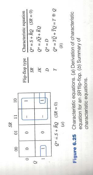
11 Characteristic Equations
12 Registers A collection of flip-flops taken as an entity. Function: Hold information within a digital system so that it is available to the logic elements during the computing process. Each combination of stored information is known as the state or content of the register. Shift register: Registers that are capable of moving information upon the occurrence of a clock-signal. Unidirectional bidirectional
13 Registers Two basic ways in which information can be entered/outputted Parallel: All 0/1 symbols handled simultaneously. Require as many lines as symbols being transferred. Serial: Involves the symbol-by-symbol availability of information in a time sequence. Four possible ways registers can transfer information: Serial-in/serial-out Serial-in/parallel-out Parallel-in/parallel-out Parallel-in/serial-out
14 Serial-in, Serial-out, Unidirectional Shift Register

15 Serial-in, Parallel-out Unidirectional Shift Register
16 Parallel-in, Parallel-out Unidirectional Shift Register

17 Universal Shift Register A bidirectional shift register. Capable of shifting contents either left or right depending upon the signals present on appropriate control input lines. Universal shift register: Depending on the signal values on the select lines of the multiplexers, the register can retain its current state, shift right, shift left or be loaded in parallel. Each operation is the result of a positive edge on the clock line.
18 Counters An example of a register. Primary purpose is to produce a specified output pattern sequence. Also called a pattern generator Each stored 0/1 combination is called the state of the counter. The total number of states is called its modulus. If a counter has m distinct states then it is called a mod-m counter. The order in which states appear is referred to as its counting sequence. Depicted by a directed graph called a state diagram.
19 State Diagram of a Counter S i denotes one of the states of the counter. Arrows in the graph denote the order in which the states occur.
20 Binary Ripple Counters Counters whose counting sequence corresponds to that of the binary numbers are called binary counters. Modulus is 2 n, where n is the number of flipflops in the counter. Binary up-counter, binary down-counter

21 4-bit Binary Ripple Counter Recall positive edge-triggered T-Flip-Flop. Each positive transition from logic-0 to logic-1 causes the flip-flop to toggle.

22 4-bit Binary Ripple Counter
23 4-bit Binary Ripple Counter Known as a ripple counter since a change in the state of the Q i 1 flip-flop is used to toggle the Q i flip-flop. The effect of a count pulse must ripple through the counter. Ripple counters also referred to as asynchronous counters. Propagation Delay There is a propagation delay between the input and output of a flip-flop. Rippling behavior affects the overall time delay between the occurrence of a count pulse and when the stabilized count appears at the output terminals. Worst Case? Going from to since toggle signals must propagate through the entire length of the counter. For n-stage binary ripple counter, the worst case time is n t pd, where t pd is the propagation delay time associated with each flip-flop.
24 Synchronous Binary Counters All flip-flops change simultaneously after the appropriate propagation delay associated with a single flip-flop. Count pulses are applied directly to the control inputs, C, of all the clocked flip-flops. All flip-flops change simultaneously after the appropriate propagation delay associated with a single flip-flop.
25 Synchronous Binary Counters The and gate preceding each input T detects if all lower-order bits are in 1-state. If yes, toggles on positive clock edge. Drawback: And gates have many inputs. Output of AND gate preceding the ith flip flop consists of the inputs fo the and-gate preceding the i 1 st flip-flop and the output Q i 1.
26 Mod-m Counter Use a mod-2 n counter as a mod-m counter. Load an initial binary number prior to the counting operation. Counter structure is modified to allow for parallel loading. JK flip-flops are used instead of T flip-flops. Two enable signals: Load enable: Allows parallel loading of data inputs D 0, D 1, D 2, D 3 Count enable: allows for counting.
27 Mod-m Counter JK flip-flops are used. Two enable signals: One to allow parallel loading of the data inputs D 0, D 1, D 2, D 3 and a second for counting. Operations synchronized with positive edges of the count pulses. The load function takes precedence over the count function (due to NOT-gate connected to the load enable line).
28 Mod-10 Counter
Chapter 6. Flip-Flops and Simple Flip-Flop Applications
 Chapter 6 Flip-Flops and Simple Flip-Flop Applications Basic bistable element It is a circuit having two stable conditions (states). It can be used to store binary symbols. J. C. Huang, 2004 Digital Logic
Experiment 8 Introduction to Latches and Flip-Flops and registers
 Experiment 8 Introduction to Latches and Flip-Flops and registers Introduction: The logic circuits that have been used until now were combinational logic circuits since the output of the device depends
Counters
 Counters A counter is the most versatile and useful subsystems in the digital system. A counter driven by a clock can be used to count the number of clock cycles. Since clock pulses occur at known intervals,
Counter dan Register
 Counter dan Register Introduction Circuits for counting events are frequently used in computers and other digital systems. Since a counter circuit must remember its past states, it has to possess memory.
D Latch (Transparent Latch)
") D Latch (Transparent Latch) -One way to eliminate the undesirable condition of the indeterminate state in the SR latch is to ensure that inputs S and R are never equal to 1 at the same time. This is done
D Latch (Transparent Latch) -One way to eliminate the undesirable condition of the indeterminate state in the SR latch is to ensure that inputs S and R are never equal to 1 at the same time. This is done
Asynchronous (Ripple) Counters
 Counters") Circuits for counting events are frequently used in computers and other digital systems. Since a counter circuit must remember its past states, it has to possess memory. The chapter about flip-flops introduced
Circuits for counting events are frequently used in computers and other digital systems. Since a counter circuit must remember its past states, it has to possess memory. The chapter about flip-flops introduced
RS flip-flop using NOR gate
 RS flip-flop using NOR gate Triggering and triggering methods Triggering : Applying train of pulses, to set or reset the memory cell is known as Triggering. Triggering methods:- There are basically two
RS flip-flop using NOR gate
 RS flip-flop using NOR gate Triggering and triggering methods Triggering : Applying train of pulses, to set or reset the memory cell is known as Triggering. Triggering methods:- There are basically two
ASYNCHRONOUS COUNTER CIRCUITS
 ASYNCHRONOUS COUNTER CIRCUITS Asynchronous counters do not have a common clock that controls all the Hipflop stages. The control clock is input into the first stage, or the LSB stage of the counter. The
Lecture 8: Sequential Logic
 Lecture 8: Sequential Logic Last lecture discussed how we can use digital electronics to do combinatorial logic we designed circuits that gave an immediate output when presented with a given set of inputs
Unit 11. Latches and Flip-Flops
 Unit 11 Latches and Flip-Flops 1 Combinational Circuits A combinational circuit consists of logic gates whose outputs, at any time, are determined by combining the values of the inputs. For n input variables,
Logic and Computer Design Fundamentals. Chapter 7. Registers and Counters
 Logic and Computer Design Fundamentals Chapter 7 Registers and Counters Registers Register a collection of binary storage elements In theory, a register is sequential logic which can be defined by a state
CHAPTER1: Digital Logic Circuits
 CS224: Computer Organization S.KHABET CHAPTER1: Digital Logic Circuits 1 Sequential Circuits Introduction Composed of a combinational circuit to which the memory elements are connected to form a feedback
Digital Fundamentals: A Systems Approach
 Digital Fundamentals: A Systems Approach Counters Chapter 8 A System: Digital Clock Digital Clock: Counter Logic Diagram Digital Clock: Hours Counter & Decoders Finite State Machines Moore machine: One
EKT 121/4 ELEKTRONIK DIGIT 1
 EKT 2/4 ELEKTRONIK DIGIT Kolej Universiti Kejuruteraan Utara Malaysia Sequential Logic Circuits - COUNTERS - LATCHES (review) S-R R Latch S-R R Latch Active-LOW input INPUTS OUTPUTS S R Q Q COMMENTS Q
Sequential Logic Counters and Registers
 Sequential Logic ounters and Registers ounters Introduction: ounters Asynchronous (Ripple) ounters Asynchronous ounters with MOD number < 2 n Asynchronous Down ounters ascading Asynchronous ounters svbitec.wordpress.com
UNIT-3: SEQUENTIAL LOGIC CIRCUITS
 UNIT-3: SEQUENTIAL LOGIC CIRCUITS STRUCTURE 3. Objectives 3. Introduction 3.2 Sequential Logic Circuits 3.2. NAND Latch 3.2.2 RS Flip-Flop 3.2.3 D Flip-Flop 3.2.4 JK Flip-Flop 3.2.5 Edge Triggered RS Flip-Flop
Logic Design. Flip Flops, Registers and Counters
 Logic Design Flip Flops, Registers and Counters Introduction Combinational circuits: value of each output depends only on the values of inputs Sequential Circuits: values of outputs depend on inputs and
CHAPTER 6 COUNTERS & REGISTERS
 CHAPTER 6 COUNTERS & REGISTERS 6.1 Asynchronous Counter 6.2 Synchronous Counter 6.3 State Machine 6.4 Basic Shift Register 6.5 Serial In/Serial Out Shift Register 6.6 Serial In/Parallel Out Shift Register
Registers and Counters
 Registers and Counters Clocked sequential circuit = F/Fs and combinational gates Register Group of flip-flops (share a common clock and capable of storing one bit of information) Consist of a group of
Chapter 4. Logic Design
 Chapter 4 Logic Design 4.1 Introduction. In previous Chapter we studied gates and combinational circuits, which made by gates (AND, OR, NOT etc.). That can be represented by circuit diagram, truth table
Universal Asynchronous Receiver- Transmitter (UART)
") Universal Asynchronous Receiver- Transmitter (UART) (UART) Block Diagram Four-Bit Bidirectional Shift Register Shift Register Counters Shift registers can form useful counters by recirculating a pattern
Universal Asynchronous Receiver- Transmitter (UART) (UART) Block Diagram Four-Bit Bidirectional Shift Register Shift Register Counters Shift registers can form useful counters by recirculating a pattern
Computer Organization & Architecture Lecture #5
 Computer Organization & Architecture Lecture #5 Shift Register A shift register is a register in which binary data can be stored and then shifted left or right when a shift signal is applied. Bits shifted
Sri Vidya College of Engineering And Technology. Virudhunagar Department of Electrical and Electronics Engineering
 Sri Vidya College of Engineering And Technology Virudhunagar 626 005 Department of Electrical and Electronics Engineering Year/ Semester/ Class : II/ III/ EEE Academic Year: 2017-2018 Subject Code/ Name:
UNIT III. Combinational Circuit- Block Diagram. Sequential Circuit- Block Diagram
 UNIT III INTRODUCTION In combinational logic circuits, the outputs at any instant of time depend only on the input signals present at that time. For a change in input, the output occurs immediately. Combinational
YEDITEPE UNIVERSITY DEPARTMENT OF COMPUTER ENGINEERING. EXPERIMENT VIII: FLIP-FLOPS, COUNTERS 2014 Fall
 YEDITEPE UNIVERSITY DEPARTMENT OF COMPUTER ENGINEERING EXPERIMENT VIII: FLIP-FLOPS, COUNTERS 2014 Fall Objective: - Dealing with the operation of simple sequential devices. Learning invalid condition in
Lecture 12. Amirali Baniasadi
 CENG 24 Digital Design Lecture 2 Amirali Baniasadi amirali@ece.uvic.ca This Lecture Chapter 6: Registers and Counters 2 Registers Sequential circuits are classified based in their function, e.g., registers.
Review of digital electronics. Storage units Sequential circuits Counters Shifters
 Review of digital electronics Storage units Sequential circuits ounters Shifters ounting in Binary A counter can form the same pattern of 0 s and 1 s with logic levels. The first stage in the counter represents
Vignana Bharathi Institute of Technology UNIT 4 DLD
 DLD UNIT IV Synchronous Sequential Circuits, Latches, Flip-flops, analysis of clocked sequential circuits, Registers, Shift registers, Ripple counters, Synchronous counters, other counters. Asynchronous
SEQUENTIAL LOGIC. Satish Chandra Assistant Professor Department of Physics P P N College, Kanpur
 SEQUENTIAL LOGIC Satish Chandra Assistant Professor Department of Physics P P N College, Kanpur www.satish0402.weebly.com OSCILLATORS Oscillators is an amplifier which derives its input from output. Oscillators
Serial In/Serial Left/Serial Out Operation
 Shift Registers The need to storage binary data was discussed earlier. In digital circuits multi-bit data has to be stored temporarily until it is processed. A flip-flop is able to store a single binary
Analysis of Sequential Circuits
 NOTE: Explanation Refer lass Notes Digital ircuits(15ee23) Analysis of Sequential ircuits by Nagaraj Vannal, Asst.Professor, School of Electronics Engineering,.L.E. Technological University, Hubballi.
Chapter 7 Counters and Registers
 Chapter 7 Counters and Registers Chapter 7 Objectives Selected areas covered in this chapter: Operation & characteristics of synchronous and asynchronous counters. Analyzing and evaluating various types
MC9211 Computer Organization
 MC9211 Computer Organization Unit 2 : Combinational and Sequential Circuits Lesson2 : Sequential Circuits (KSB) (MCA) (2009-12/ODD) (2009-10/1 A&B) Coverage Lesson2 Outlines the formal procedures for the
Registers and Counters
 Registers and Counters Clocked sequential circuit = F/Fs and combinational gates Register Group of flip-flops (share a common clock and capable of storing one bit of information) Consist of a group of
CHAPTER 4: Logic Circuits
 CHAPTER 4: Logic Circuits II. Sequential Circuits Combinational circuits o The outputs depend only on the current input values o It uses only logic gates, decoders, multiplexers, ALUs Sequential circuits
Flip-Flops. Because of this the state of the latch may keep changing in circuits with feedback as long as the clock pulse remains active.
 Flip-Flops Objectives The objectives of this lesson are to study: 1. Latches versus Flip-Flops 2. Master-Slave Flip-Flops 3. Timing Analysis of Master-Slave Flip-Flops 4. Different Types of Master-Slave
Digital Systems Laboratory 3 Counters & Registers Time 4 hours
 Digital Systems Laboratory 3 Counters & Registers Time 4 hours Aim: To investigate the counters and registers constructed from flip-flops. Introduction: In the previous module, you have learnt D, S-R,
Synchronous Sequential Logic
 Synchronous Sequential Logic -A Sequential Circuit consists of a combinational circuit to which storage elements are connected to form a feedback path. The storage elements are devices capable of storing
CHAPTER 4: Logic Circuits
 CHAPTER 4: Logic Circuits II. Sequential Circuits Combinational circuits o The outputs depend only on the current input values o It uses only logic gates, decoders, multiplexers, ALUs Sequential circuits
VTU NOTES QUESTION PAPERS NEWS RESULTS FORUMS Registers
 Registers Registers are a very important digital building block. A data register is used to store binary information appearing at the output of an encoding matrix.shift registers are a type of sequential
ELCT201: DIGITAL LOGIC DESIGN
 ELCT201: DIGITAL LOGIC DESIGN Dr. Eng. Haitham Omran, haitham.omran@guc.edu.eg Dr. Eng. Wassim Alexan, wassim.joseph@guc.edu.eg Lecture 6 Following the slides of Dr. Ahmed H. Madian ذو الحجة 1438 ه Winter
Flip Flop. S-R Flip Flop. Sequential Circuits. Block diagram. Prepared by:- Anwar Bari
 Sequential Circuits The combinational circuit does not use any memory. Hence the previous state of input does not have any effect on the present state of the circuit. But sequential circuit has memory
UNIT IV. Sequential circuit
 UNIT IV Sequential circuit Introduction In the previous session, we said that the output of a combinational circuit depends solely upon the input. The implication is that combinational circuits have no
ELCT201: DIGITAL LOGIC DESIGN
 ELCT201: DIGITAL LOGIC DESIGN Dr. Eng. Haitham Omran, haitham.omran@guc.edu.eg Dr. Eng. Wassim Alexan, wassim.joseph@guc.edu.eg Lecture 7 Following the slides of Dr. Ahmed H. Madian محرم 1439 ه Winter
Logic Design II (17.342) Spring Lecture Outline
 Spring Lecture Outline") Logic Design II (17.342) Spring 2012 Lecture Outline Class # 05 February 23, 2012 Dohn Bowden 1 Today s Lecture Analysis of Clocked Sequential Circuits Chapter 13 2 Course Admin 3 Administrative Admin
Logic Design II (17.342) Spring 2012 Lecture Outline Class # 05 February 23, 2012 Dohn Bowden 1 Today s Lecture Analysis of Clocked Sequential Circuits Chapter 13 2 Course Admin 3 Administrative Admin
Flip-Flops and Related Devices. Wen-Hung Liao, Ph.D. 4/11/2001
 Flip-Flops and Related Devices Wen-Hung Liao, Ph.D. 4/11/2001 Objectives Recognize the various IEEE/ANSI flip-flop symbols. Use state transition diagrams to describe counter operation. Use flip-flops in
(CSC-3501) Lecture 7 (07 Feb 2008) Seung-Jong Park (Jay) CSC S.J. Park. Announcement
 Lecture 7 (07 Feb 2008) Seung-Jong Park (Jay) CSC S.J. Park. Announcement") Seung-Jong Park (Jay) http://www.csc.lsu.edu/~sjpark Computer Architecture (CSC-3501) Lecture 7 (07 Feb 2008) 1 Announcement 2 1 Combinational vs. Sequential Logic Combinational Logic Memoryless Outputs
Seung-Jong Park (Jay) http://www.csc.lsu.edu/~sjpark Computer Architecture (CSC-3501) Lecture 7 (07 Feb 2008) 1 Announcement 2 1 Combinational vs. Sequential Logic Combinational Logic Memoryless Outputs
Digital Circuits ECS 371
 igital Circuits ECS 371 r. Prapun Suksompong prapun@siit.tu.ac.th Lecture 17 Office Hours: BK 3601-7 Monday 9:00-10:30, 1:30-3:30 Tuesday 10:30-11:30 1 Announcement Reading Assignment: Chapter 7: 7-1,
2. Counter Stages or Bits output bits least significant bit (LSB) most significant bit (MSB) 3. Frequency Division 4. Asynchronous Counters
 most significant bit (MSB) 3. Frequency Division 4. Asynchronous Counters") 2. Counter Stages or Bits The number of output bits of a counter is equal to the flip-flop stages of the counter. A MOD-2 n counter requires n stages or flip-flops in order to produce a count sequence
2. Counter Stages or Bits The number of output bits of a counter is equal to the flip-flop stages of the counter. A MOD-2 n counter requires n stages or flip-flops in order to produce a count sequence
NH 67, Karur Trichy Highways, Puliyur C.F, Karur District UNIT-III SEQUENTIAL CIRCUITS
 NH 67, Karur Trichy Highways, Puliyur C.F, 639 114 Karur District DEPARTMENT OF ELETRONICS AND COMMUNICATION ENGINEERING COURSE NOTES SUBJECT: DIGITAL ELECTRONICS CLASS: II YEAR ECE SUBJECT CODE: EC2203
DIGITAL SYSTEM FUNDAMENTALS (ECE421) DIGITAL ELECTRONICS FUNDAMENTAL (ECE422) COUNTERS
 DIGITAL ELECTRONICS FUNDAMENTAL (ECE422) COUNTERS") COURSE / CODE DIGITAL SYSTEM FUNDAMENTALS (ECE421) DIGITAL ELECTRONICS FUNDAMENTAL (ECE422) COUNTERS One common requirement in digital circuits is counting, both forward and backward. Digital clocks and
COURSE / CODE DIGITAL SYSTEM FUNDAMENTALS (ECE421) DIGITAL ELECTRONICS FUNDAMENTAL (ECE422) COUNTERS One common requirement in digital circuits is counting, both forward and backward. Digital clocks and
ECE 341. Lecture # 2
 ECE 341 Lecture # 2 Instructor: Zeshan Chishti zeshan@pdx.edu October 1, 2014 Portland State University Announcements Course website reminder: http://www.ece.pdx.edu/~zeshan/ece341.htm Homework 1: Will
Advanced Devices. Registers Counters Multiplexers Decoders Adders. CSC258 Lecture Slides Steve Engels, 2006 Slide 1 of 20
 Advanced Devices Using a combination of gates and flip-flops, we can construct more sophisticated logical devices. These devices, while more complex, are still considered fundamental to basic logic design.
UNIVERSITI TEKNOLOGI MALAYSIA
 SULIT Faculty of Computing UNIVERSITI TEKNOLOGI MALAYSIA FINAL EXAMINATION SEMESTER I, 2016 / 2017 SUBJECT CODE : SUBJECT NAME : SECTION : TIME : DATE/DAY : VENUES : INSTRUCTIONS : Answer all questions
LSN 12 Shift Registers
 LSN 12 Shift Registers Department of Engineering Technology LSN 12 Shift Registers Digital circuits with data storage and data movement functions Storage capacity is the total number of bits of digital
Digital Design, Kyung Hee Univ. Chapter 5. Synchronous Sequential Logic
 Chapter 5. Synchronous Sequential Logic 1 5.1 Introduction Electronic products: ability to send, receive, store, retrieve, and process information in binary format Dependence on past values of inputs Sequential
IT T35 Digital system desigm y - ii /s - iii
 UNIT - III Sequential Logic I Sequential circuits: latches flip flops analysis of clocked sequential circuits state reduction and assignments Registers and Counters: Registers shift registers ripple counters
Chapter 6 Digital Circuit 6-5 Department of Mechanical Engineering
 MEMS1082 Chapter 6 Digital Circuit 6-5 General digital system D Flip-Flops, The D flip-flop is a modification of the clocked SR flip-flop. The D input goes directly into the S input and the complement
Final Exam review: chapter 4 and 5. Supplement 3 and 4
 Final Exam review: chapter 4 and 5. Supplement 3 and 4 1. A new type of synchronous flip-flop has the following characteristic table. Find the corresponding excitation table with don t cares used as much
Slide 1. Flip-Flops. Cross-NOR SR flip-flop S R Q Q. hold reset set not used. Cross-NAND SR flip-flop S R Q Q. not used reset set hold 1 Q.
 Slide Flip-Flops Cross-NOR SR flip-flop Reset Set Cross-NAND SR flip-flop Reset Set S R reset set not used S R not used reset set 6.7 Digital ogic Slide 2 Clocked evel-triggered NAND SR Flip-Flop S R SR
Logic Design II (17.342) Spring Lecture Outline
 Spring Lecture Outline") Logic Design II (17.342) Spring 2012 Lecture Outline Class # 03 February 09, 2012 Dohn Bowden 1 Today s Lecture Registers and Counters Chapter 12 2 Course Admin 3 Administrative Admin for tonight Syllabus
Logic Design II (17.342) Spring 2012 Lecture Outline Class # 03 February 09, 2012 Dohn Bowden 1 Today s Lecture Registers and Counters Chapter 12 2 Course Admin 3 Administrative Admin for tonight Syllabus
COSC 243. Sequential Logic. COSC 243 (Computer Architecture) Lecture 5 - Sequential Logic 1
 Lecture 5 - Sequential Logic 1") COC 243 equential Logic COC 243 (Computer Architecture) Lecture 5 - equential Logic 1 Overview Last Lecture This Lecture equential logic circuits ource: Chapter 11 (10 th edition) Next Lecture Computer
COC 243 equential Logic COC 243 (Computer Architecture) Lecture 5 - equential Logic 1 Overview Last Lecture This Lecture equential logic circuits ource: Chapter 11 (10 th edition) Next Lecture Computer
More on Flip-Flops Digital Design and Computer Architecture: ARM Edition 2015 Chapter 3 <98> 98
 More on Flip-Flops Digital Design and Computer Architecture: ARM Edition 2015 Chapter 3 98 Review: Bit Storage SR latch S (set) Q R (reset) Level-sensitive SR latch S S1 C R R1 Q D C S R D latch Q
Chapter. Synchronous Sequential Circuits
 Chapter 5 Synchronous Sequential Circuits Logic Circuits- Review Logic Circuits 2 Combinational Circuits Consists of logic gates whose outputs are determined from the current combination of inputs. Performs
EE292: Fundamentals of ECE
 EE292: Fundamentals of ECE Fall 2012 TTh 10:00-11:15 SEB 1242 Lecture 23 121120 http://www.ee.unlv.edu/~b1morris/ee292/ 2 Outline Review Combinatorial Logic Sequential Logic 3 Combinatorial Logic Circuits
EET2411 DIGITAL ELECTRONICS
 5-8 Clocked D Flip-FlopFlop One data input. The output changes to the value of the input at either the positive going or negative going clock trigger. May be implemented with a J-K FF by tying the J input
Sequential Digital Design. Laboratory Manual. Experiment #7. Counters
 The Islamic University of Gaza Engineering Faculty Department of Computer Engineering Spring 2018 ECOM 2022 Khaleel I. Shaheen Sequential Digital Design Laboratory Manual Experiment #7 Counters Objectives
Sequential circuits. Same input can produce different output. Logic circuit. William Sandqvist
 Sequential circuits Same input can produce different output Logic circuit If the same input may produce different output signal, we have a sequential logic circuit. It must then have an internal memory
Switching Theory And Logic Design UNIT-IV SEQUENTIAL LOGIC CIRCUITS
 Switching Theory And Logic Design UNIT-IV SEQUENTIAL LOGIC CIRCUITS Sequential circuits Classification of sequential circuits: Sequential circuits may be classified as two types. 1. Synchronous sequential
 UNIT 1 NUMBER SYSTEMS AND DIGITAL LOGIC FAMILIES 1. Briefly explain the stream lined method of converting binary to decimal number with example. 2. Give the Gray code for the binary number (111) 2. 3.
MODU LE DAY. Class-A, B, AB and C amplifiers - basic concepts, power, efficiency Basic concepts of Feedback and Oscillation. Day 1
 DAY MODU LE TOPIC QUESTIONS Day 1 Day 2 Day 3 Day 4 I Class-A, B, AB and C amplifiers - basic concepts, power, efficiency Basic concepts of Feedback and Oscillation Phase Shift Wein Bridge oscillators.
Introduction. NAND Gate Latch. Digital Logic Design 1 FLIP-FLOP. Digital Logic Design 1
 2007 Introduction BK TP.HCM FLIP-FLOP So far we have seen Combinational Logic The output(s) depends only on the current values of the input variables Here we will look at Sequential Logic circuits The
Chapter 2. Digital Circuits
 Chapter 2. Digital Circuits Logic gates Flip-flops FF registers IC registers Data bus Encoders/Decoders Multiplexers Troubleshooting digital circuits Most contents of this chapter were covered in 88-217
Other Flip-Flops. Lecture 27 1
 Other Flip-Flops Other types of flip-flops can be constructed by using the D flip-flop and external logic. Two flip-flops less widely used in the design of digital systems are the JK and T flip-flops.
DIGITAL CIRCUIT LOGIC UNIT 11: SEQUENTIAL CIRCUITS (LATCHES AND FLIP-FLOPS)
") DIGITAL CIRCUIT LOGIC UNIT 11: SEQUENTIAL CIRCUITS (LATCHES AND FLIP-FLOPS) 1 iclicker Question 16 What should be the MUX inputs to implement the following function? (4 minutes) f A, B, C = m(0,2,5,6,7)
DIGITAL CIRCUIT LOGIC UNIT 11: SEQUENTIAL CIRCUITS (LATCHES AND FLIP-FLOPS) 1 iclicker Question 16 What should be the MUX inputs to implement the following function? (4 minutes) f A, B, C = m(0,2,5,6,7)
CS T34-DIGITAL SYSTEM DESIGN Y2/S3
 UNIT III Sequential Logic: Latches versus Flip Flops SR, D, JK, Master Slave Flip Flops Excitation table Conversion of Flip flops Counters: Asynchronous, synchronous, decade, presettable Shift Registers:
Chapter 8 Sequential Circuits
 Philadelphia University Faculty of Information Technology Department of Computer Science Computer Logic Design By 1 Chapter 8 Sequential Circuits 1 Classification of Combinational Logic 3 Sequential circuits
ELE2120 Digital Circuits and Systems. Tutorial Note 7
 ELE2120 Digital Circuits and Systems Tutorial Note 7 Outline 1. Sequential Circuit 2. Gated SR Latch 3. Gated D-latch 4. Edge-Triggered D Flip-Flop 5. Asynchronous and Synchronous reset Sequential Circuit
Flip-Flops and Sequential Circuit Design
 Flip-Flops and Sequential Circuit Design ECE 52 Summer 29 Reading ssignment Brown and Vranesic 7 Flip-Flops, Registers, Counters and a Simple Processor 7.5 T Flip-Flop 7.5. Configurable Flip-Flops 7.6
Digital Fundamentals
 igital Fundamentals Tenth Edition Floyd Chapter 7 Modified by Yuttapong Jiraraksopakun Floyd, igital Fundamentals, 10 th 2008 Pearson Education ENE, KMUTT ed 2009 Summary Latches A latch is a temporary
Chapter 6 Registers and Counters
 EEA051 - Digital Logic 數位邏輯 Chapter 6 Registers and Counters 吳俊興國立高雄大學資訊工程學系 January 2006 Chapter 6 Registers and Counters 6-1 Registers 6-2 Shift Registers 6-3 Ripple Counters 6-4 Synchronous Counters
Module -5 Sequential Logic Design
 Module -5 Sequential Logic Design 5.1. Motivation: In digital circuit theory, sequential logic is a type of logic circuit whose output depends not only on the present value of its input signals but on
Chapter 5: Synchronous Sequential Logic
 Chapter 5: Synchronous Sequential Logic NCNU_2016_DD_5_1 Digital systems may contain memory for storing information. Combinational circuits contains no memory elements the outputs depends only on the inputs
Part II. Chapter2: Synchronous Sequential Logic
 課程名稱 : 數位系統設計導論 P-/77 Part II Chapter2: Synchronous Sequential Logic 教師 : 郭峻因教授 INSTRUCTOR: Prof. Jiun-In Guo E-mail: jiguo@cs.ccu.edu.tw 課程名稱 : 數位系統設計導論 P-2/77 Special thanks to Prof. CHING-LING SU for
Digital Logic Design Sequential Circuits. Dr. Basem ElHalawany
 Digital Logic Design Sequential Circuits Dr. Basem ElHalawany Combinational vs Sequential inputs X Combinational Circuits outputs Z A combinational circuit: At any time, outputs depends only on inputs
1. Convert the decimal number to binary, octal, and hexadecimal.
 1. Convert the decimal number 435.64 to binary, octal, and hexadecimal. 2. Part A. Convert the circuit below into NAND gates. Insert or remove inverters as necessary. Part B. What is the propagation delay
Chapter 5 Synchronous Sequential Logic
 Chapter 5 Synchronous Sequential Logic Chih-Tsun Huang ( 黃稚存 ) http://nthucad.cs.nthu.edu.tw/~cthuang/ Department of Computer Science National Tsing Hua University Outline Introduction Storage Elements:
Synchronous Sequential Logic
 Synchronous Sequential Logic Ranga Rodrigo August 2, 2009 1 Behavioral Modeling Behavioral modeling represents digital circuits at a functional and algorithmic level. It is used mostly to describe sequential
MODULE 3. Combinational & Sequential logic
 MODULE 3 Combinational & Sequential logic Combinational Logic Introduction Logic circuit may be classified into two categories. Combinational logic circuits 2. Sequential logic circuits A combinational
COE 202: Digital Logic Design Sequential Circuits Part 1. Dr. Ahmad Almulhem ahmadsm AT kfupm Phone: Office:
 COE 202: Digital Logic Design Sequential Circuits Part 1 Dr. Ahmad Almulhem Email: ahmadsm AT kfupm Phone: 860-7554 Office: 22-324 Objectives Sequential Circuits Memory Elements Latches Flip-Flops Combinational
CMSC 313 Preview Slides
 CMSC 33 Preview Slides These are draft slides. The actual slides presented in lecture may be different due to last minute changes, schedule slippage,... UMBC, CMSC33, Richard Chang CMSC
 WWW.STUDENTSFOCUS.COM + Class Subject Code Subject Prepared By Lesson Plan for Time: Lesson. No 1.CONTENT LIST: Introduction to Unit III 2. SKILLS ADDRESSED: Listening I year, 02 sem CS6201 Digital Principles
Sequential Logic. E&CE 223 Digital Circuits and Systems (A. Kennings) Page 1
 Page 1") Sequential Logic E&CE 223 igital Circuits and Systems (A. Kennings) Page 1 Sequential Circuits Have considered only combinational circuits in which circuit outputs are determined entirely by current circuit
Sequential Logic E&CE 223 igital Circuits and Systems (A. Kennings) Page 1 Sequential Circuits Have considered only combinational circuits in which circuit outputs are determined entirely by current circuit
EEE2135 Digital Logic Design Chapter 6. Latches/Flip-Flops and Registers/Counters 서강대학교 전자공학과
 EEE235 Digital Logic Design Chapter 6. Latches/Flip-Flops and Registers/Counters 서강대학교 전자공학과 . Delay and Latches ) Signal Storage a. as voltage level static memory b. as charges dynamic memory 2) Delays
Logic Design Viva Question Bank Compiled By Channveer Patil
 Logic Design Viva Question Bank Compiled By Channveer Patil Title of the Practical: Verify the truth table of logic gates AND, OR, NOT, NAND and NOR gates/ Design Basic Gates Using NAND/NOR gates. Q.1
(Refer Slide Time: 2:00)
") Digital Circuits and Systems Prof. Dr. S. Srinivasan Department of Electrical Engineering Indian Institute of Technology, Madras Lecture #21 Shift Registers (Refer Slide Time: 2:00) We were discussing
Digital Circuits and Systems Prof. Dr. S. Srinivasan Department of Electrical Engineering Indian Institute of Technology, Madras Lecture #21 Shift Registers (Refer Slide Time: 2:00) We were discussing
Engr354: Digital Logic Circuits
 Engr354: igital Circuits Chapter 7 Sequential Elements r. Curtis Nelson Sequential Elements In this chapter you will learn about: circuits that can store information; Basic cells, latches, and flip-flops;
Unit 9 Latches and Flip-Flops. Dept. of Electrical and Computer Eng., NCTU 1
 Unit 9 Latches and Flip-Flops Dept. of Electrical and Computer Eng., NCTU 1 9.1 Introduction Dept. of Electrical and Computer Eng., NCTU 2 What is the characteristic of sequential circuits in contrast
CprE 281: Digital Logic
 CprE 28: Digital Logic Instructor: Alexander Stoytchev http://www.ece.iastate.edu/~alexs/classes/ Registers and Counters CprE 28: Digital Logic Iowa State University, Ames, IA Copyright Alexander Stoytchev