A Simple VGA Interface for the PowerPC 403GCX Evaluation Board
|
|
|
- Godwin Barber
- 6 years ago
- Views:
Transcription
1 A Simple VGA Interface for the PowerPC 403GCX Evaluation Board Jonathan Jones, Undergraduate Department of Computer Science Texas A & M University Completed January 23, 2001
2 Table of Contents I. Abstract II. Hardware Requirements Figure 1. Abstract wiring diagram Table 1. Wire connections Figure 2. Pinouts for connectors and components III. Demonstrating the VGA Interface s Functions Figure 3. Academic building in four shades of gray Figure 4. Three frames to be page-flipped IV. Programming the VGA Interface Table GCX register settings Table 3. VGA interface memory map Table 4. Format of color registers V. Implementation of the VGA Interface Figure 5. Diagram showing functional units, signals Figure 6. State diagram for BUSCTL Figure 7. Timing diagram for memory write cycle Figure 8. State diagram for MEMCTRL Table 5. Descriptions of timing parameters VI. Possible Future Projects VII. References Appendices A. XS40 V1.1 documentation B. PPC 403 EVB expansion interface pinout C. 74ALS245 bus transceivers documentation D MHz clock oscillator documentation E. XStend V1.3 documentation F. VGA signal generation with the XS board G. VHDL source code for VGACORE module H. Documentation for SRAM module I. FPGA design schematics J. IBM 403GCX embedded controller manual K. Photographs 2
3 I. Abstract This report describes the author s implementation of a VGA monitor interface for the PowerPC 403GCX evaluation board. Additional hardware used for the project essentially consists of a Xilinx[1] FPGA, a 32KB SRAM module, a few resistors (forming a simple DAC), and a VGA monitor connector. These components are all included on prototyping boards available from XESS Corp[2]. Because of the limited pinout of the FPGA chosen for the project, three bus transcievers are needed as well. A 24.0 MHz oscillator is used to clock the circuit. The VGA interface implemented allows the display of a 512 by 240 pixel image with four user-definable colors. It also includes a vertical offset register to facilitate hardware scrolling. Programs running on the 403GCX can update the registers and SRAM by using store instructions. II. Hardware Requirements The required hardware components, in addition to the PowerPC 403GCX evaluation board, are the following: 1. One XESS Corp. XS40 prototyping board. The implementation described herein uses a Version 1.1 board, which includes a Xilinx XC4010XL FPGA. Other versions of the XS40 with other FPGAs will work, but may require different jumper settings. Compare your board s documentation with the Version 1.1 jumper settings listed below (in Part III ). If you don t have an XS40 board, you can wire up your own FPGA, SRAM, power supply, and FPGA programming interface according to the XS40 s schematics. (The XS40 s other components are not used.) Complete Documentation for the XS40 V1.1 is included as Appendix A. 2. One XESS Corp. XStend board, which provides the VGA connector and DAC, and provides header pins to make it easier to wire wrap to the XS40 s pins. Versions 1.2 and above of the XS40 include the VGA connector and DAC onboard and make the XStend unnecessary for this application. This implementation was tested using the XStend V1.3; other versions may require different jumper settings. 3. One 24.0 MHz crystal oscillator clocks the circuit on the FPGA. Some versions of the XS40 include a 12.0 MHz oscillator, which 3
4 isn t fast enough for this application. Others include a programmable oscillator which can t be programmed to operate at 24.0 MHz. 4. Three octal bus transcievers. The specific part used for testing this implementation was the SN74ALS245AN from Texas Instruments. If you want to use a slower part, you may have to adjust the number of wait states in the BUSCTL state machine (Part IV). These transcievers isolate the 403GCX s address and data buses from those of the SRAM. If you use an FPGA with a larger pinout, you can eliminate the need for these by connecting all bus lines directly to the FPGA, using separate pins for the SRAM s buses and the 403GCX s buses. 5. One 5V power supply for powering the bus transcievers. The XS40 s power supply does not appear capable of powering them while still enabling the oscillator to provide a clean and consistent signal. 6. A breadboard and wiring to connect everything together and to the PowerPC 403GCX evaluation board s expansion interface. For testing, the following will also be needed: 7. Any VGA monitor. The signals output by the VGA interface are compatible with all VGA monitors. 8. The IBM RISCWatch debugger system. Installation and operation of this system is described in a previous report[3], and further documentation is available on IBM s Web site[4]. It is basically a hardware/software interface to allow a PC to communicate directly with the PowerPC 403GCX through its JTAG testing interface. This allows the 403GCX s I/O Configuration Register (IOCR) and Bank Registers (BRn) to be set, so the 403GCX will know how to access the VGA interface s memory. Then RISCWatch can be used to actually load the data into display memory. Alternatively, you can write a program that sets the registers and fills the video RAM, and load this program using the evaluation board s ROM monitor. 9. A PC connected via its parallel port to the XS40 board. The PC must have XSTOOLs software (available from XESS[2]) for programming the FPGA via the parallel port. For creating.bit files (FPGA program images) you ll need Xilinx Foundation Series software (from Xilinx[1]). The latter is not free, but it is not 4
5 necessary unless you want to modify the FPGA program. If not, just use the.bit file accompanying this document. III. Assembly and Configuration Assembly consists of wiring the hardware components together. Configuration includes adding/removing shunts on the jumpers of the XS40 and XStend boards, and programming the FPGA. Pin assignments for the PowerPC 403GCX evaluation board s expansion interface, for the bus transcievers, and for the 24.0 MHz oscillator are included in Appendices B, C, and D, respectively. Pin assignments for the XS40 (whose pins are exposed by the XStend) can be found in Appendix A. Figure 1 is a wiring diagram showing how the components are connected. Each line represents a set of connections, as detailed in Table 1. Figure 1. Abstract wiring diagram. 403GCX EVB Expansion Interface MX045 A B C H 5V power supply + D J E F G - XStend Board J18 XS40 Board XS40 s parallel port interface to PC s parallel port interface to VGA monitor 9V power supply + - 5
6 Table 1. Wire connections. A B C D Exp Int Exp Int Exp Int MX045 J18 A39 18 A33 18 A B39 17 B33 17 B A31 16 C33 16 C B31 15 A34 15 A10 15 H C31 14 B34 14 B10 14 Exp Int Supply A32 13 C34 13 C10 13 C40 GND B32 12 A35 12 A11 12 C28 GND C32 11 B35 11 B E F G 1 GND J J J18 10 GND V GND GND V GND GND V J J18 Exp Int J18 52 GND B26 7 A26 37 A15 9 A40 8 B26 7 Figure 2. Pinouts for connectors and components. C40 B40 A40 PowerPC 403GCX EVB expansion interface connector C1 B1 A MX045 top view top view J18 (oriented as in Figure 1)

7 For convenience, the pinouts for all the components and connectors are shown in Figure 2. Jumpers on the XS40 and XStend board are used to select certain options and disable various unneeded components. For versions 1.1 and 1.3, respectively, of the boards, the jumpers should be configured as follows. On the XStend board, move all DIP switches to the OFF/OPEN position, and remove shunts from all jumpers except J11. This will disable all the components on the XStend board except the VGA connector and its associated DAC. On the XS40 board, shunt jumpers J4, J5 (if present), J7 (across pins 1 and 2), and J11. Remove the shunts from jumpers J6 and J10. These settings specify, among other things, that the parallel port interface will be used to program the FPGA. See section 1.6 of Appendix A for more information about jumper settings of the XS40 V1.1 board. See Appendix E for information on jumper settings for the XStend V1.3. After doing all the above, all that remains is to program the FPGA with the VGA.BIT file. Do this by using the XSLOAD or GXSLOAD program from the XSTOOLs suite. An image should appear immediately on the screen after programming. (You may have to push the RESET button on the XStend board first.) IV. Demonstrating the VGA Interface s Functions As a first demonstration, run the RISCWatch software and select Command File from the File menu. Then choose the file SCREEN1.CMD that accompanies this document. Execute the script in Normal Mode. The image in Figure 3 should be displayed on the VGA monitor. Figure 3. The Academic Building in four shades of gray. 7
.")
8 This is a 512-by-240-pixel, four-color image. The color registers are loaded with white, black, and two intermediate shades of grey. Now load the command file SCREEN2.CMD in the same manner as before. This script demonstrates the palette shifting and page flipping capabilities of the VGA interface. It first loads three 512-by-85 pixel frames into VGA memory (Figure 4). It then sets the VGA interface s HEIGHT register so that only the topmost 85 lines are displayed. To flip between the frames, it sets the VGA interface s VOFFSET (vertical offset) register to the line number of the first line of each frame. By continually updating the VOFFSET register, simple animation effects are possible. The script also illustrates another simple animation method. By changing the appropriate color register (COLORA, COLORB, COLORC, or COLORD), you can change all the pixels on the display of that color. This allows changing the color of large areas of the screen much faster than would be possible by storing a new value in memory for each pixel. Combining these effects can achieve very annoying results, as the script shows. Figure 4. Three frames to be page-flipped. V. Programming the VGA Interface Preparing the VGA interface for use entails setting two of the 403GCX s internal registers to inform the chip how to communicate with the VGA s memory. These registers are the Input/Output 8
9 Configuration Register (IOCR) and Bank Register 3 (BR3). Table 2 shows values that were tested and verified to work, though they are probably not optimal. See Part VI for an explanation of these register settings. Table GCX register settings. IOCR 0004C402 BR E After these registers are set, the VGA interface is exposed to the programmer for access according to the memory map in Table 3. Data can be stored into the display memory and the VGA interface s internal registers by standard memory write instructions. (It cannot be read, though; this memory is write-only.) Table 3. VGA Interface memory map (addresses in hex). Address(es) Size Field FFF 32KB Display memory FFF 2KB Invisible display memory B VGA interface s internal registers B COLORA register B COLORB register B COLORC register B COLORD register B VOFFSET register B HEIGHT register B (unused) B (unused) The display memory is organized as follows. Each scan line is 512 pixels wide and occupies 128 bytes of memory. This means there are four pixels in each byte of display memory. And that means each pixel is represented by two bits, which can have four possible values. Pixels with values 0, 1, 2, and 3 are colored according to the values of color registers COLORA, COLORB, COLORC, and COLORD, respectively. The first scan line starts at address ; the second starts 128 bytes later at ; and so on. The VOFFSET register holds a value between 0 and 255 allowing the programmer to scroll the screen. A value of 0 is the default, nonscrolled situation. A value of 1 indicates that the VGA interface should start reading from address instead of , effectively scrolling the screen by one scan line. 9
10 The HEIGHT register holds a value between 0 and 240 representing the number of scan lines to be displayed on the screen. A value of 240 is the default and causes the first 30 KB (240 scan lines) of display memory (starting from the address indicated by VOFFSET) to be visible. (The remaining 2 KB of display memory is invisible. ) A value of 120, for example, causes the bottom half of the screen to be blank. Values greater than 240 can be used to add scan lines below the bottom of the usual display area. The HEIGHT and VOFFSET registers can be used together to implement page flipping, as described in Part IV. VOFFSET also helps in the imelementation of text scrolling. The new text can be drawn in the invisible display memory, then scrolled into view by incrementing VOFFSET. The format of the color registers (COLORA, COLORB, COLORC, COLORD) is shown in Table 4. Table 4. Format of color registers. bit 7 (MSB) (LSB) field X X Red 1 Red 0 Green 1 Green 0 Blue 1 Blue 0 This shows that there are four levels of red, four levels of green, and four levels of blue available, for a total of 64 possible colors. This is determined by the limitations of the simple DAC available on the XStend board. The four color registers can be set independently (using byte-wide memory write instructions), so that four colors can be displayed on the screen at one time. See Part IV for an explanation of achieving animaton effects using palette shifting. VI. Implementation of the VGA interface Before beginning this section the reader should familiarize himself with Appendix F, which gives general information on the relevant VGA standard and describes an implementation of a VGA controller using the XS40. The VGACORE module specified therein is the basis, with modifications, for the VGACORE module used in the present application. The major changes applied to the original VGACORE are the following: 1. The original VGACORE only displays 256 pixels in each scan line. This isn t suitable for displaying 80-column text. 512 pixels is 10
11 sufficient (with each text character six pixels wide, and space left over at the margins). However, this requires that the pixel clock speed be doubled. The original VGACORE used the XS40 s onboard 12.0 MHz clock; the new version will require an external 24.0 MHz clock. 2. In the original VGACORE the colors are hard-wired. The new version makes use of four color registers (COLORA, COLORB, COLORC, COLORD; see Part V) to allow the colors to be changed in software. 3. A VOFFSET register was added to allow hardware scrolling to be controlled by software (see Part V). 4. A HEIGHT register was added to allow the number of scan lines in the display to be controlled by software (see Part V). 5. Since the clock speed is doubled, the SRAM is no longer fast enough to yield correct output in the span of a single clock cycle. Therefore the new VGACORE uses pipelining to allow the SRAM three clock cycles to drive its outputs before they are sampled. This change was effected by editing the process labeled I. The conditional if hcnt(1 downto 0)="00" then was changed to if hcnt(1 downto 0)="11" then Since the SRAM s address bus is driven when hcnt= 00, that gives three clock cycles before its outputs are sampled. Of course, this also required tweaking the hsyncb and blank signals to account for the pipelining delay. 6. The VGACORE module is continually reading from SRAM while the electron beams sweep across the screen. Then there is an idle period in which the beams are moved back across the screen to the beginning of the next scan line. Then after all the scan lines have been displayed, there is a much longer idle period while the beams are moved back to the top of the screen. These idle periods are utilized by the new VGACORE, via its memreq signal, to yield control of the SRAM to allow the 403GCX to access it. VGACORE drops memreq to allow the BUSCTL state machine to give control of the 403GCX access to the local address and data buses. 11
12 The VHDL source code for the new VGACORE is shown in Appendix G. To understand how the VGACORE interacts with the rest of the system, consult Figure 5. While painting the pixels on the screen, VGACORE drives the local address bus and reads the local data bus. When VGACORE yields control of the buses, BUSCTL is enabled. BUSCTL then disables the SRAM s outputs, enables the bus transcievers (thereby connecting the 403GCX to the local address and data buses), and enables the MEMCTRL unit. MEMCTRL can then communicate with the 403GCX, through the three handshaking signals shown, to oversee memory writes from the 403GCX to the SRAM and internal registers. When VGACORE is ready to paint the next scan line, it disables BUSCTL, which tri-states the bus transcievers and enables the SRAM s data outputs. MEMCTRL postpones any pending memory accesses until the next time it is READY ADDRESS BUS 403GCX DATA BUS CHIP SELECT WRITE BYTE VGA Monitor RGB SYNC Bus Transcievers ENABLE VGACORE LOCAL ADDRESS BUS LOCAL DATA BUS BUSCTL ENABLE ENABLE ENABLE WRITE ENABLE MEMCTRL REGISTERS SRAM MEMORY MODULE REGISTER VALUES FPGA Figure 5. Diagram showing functional units, data paths, and control signals. 12
13 enabled by BUSCTL. VGACORE uses its MEMREQ output to enable BUSCTL. Examine Figure 6, which shows the state diagram for BUSCTL, a finite state machine. BUSCTL waits in its VGA state until VGACORE deasserts MEMREQ. Then it disables the SRAM s data outputs, and waits in its ZWt1 state for the SRAM s data outputs to reach high impedance. Then BUSCTL enables the external bus transcievers to connect the 403GCX to the local address and data buses. After waiting in BWt for the buses to be driven, it asserts MC_ENABLE, which gives control of the buses to the MEMCTRL module. When VGACORE needs access to memory again, it asserts MEMREQ. BUSCTL immediately deasserts MC_ENABLE, disables the bus transcievers (thus isolating the 403GCX from the local buses), and enables the SRAM s data outputs. The cycle repeats. BUSCTL //diagram ACTIONS RESET CLOCK MEMREQ MC_ENABLE BUF_OEN SRAM_OEN Sreg0 W t RESET= 1 SRAM_OEN <= 1 ; BUF_OEN <= 1 ; MC_ENABLE <= 0 ; VGA /0/ Wt >= 5 MEMREQ = 0 SRAM_OEN <= 1 ; Wt := 0; Wt := W t + 1; ZWt1 /1/ Wt >= 5 BUF_OEN <= 0 ; Wt := 0; W t := Wt + 1; BWt /2/ Wt >= 5 MC_ENABLE <= 1 ; SWt /5/ Wt := W t + 1; Wt >= 5 SRAM_OEN <= 0 ; Wt := 0; ZWt2 /4/ Wt := Wt + 1; MEMREQ = 1 MC_ENABLE <= 0 ; BUF_OEN <= 1 ; Wt := 0; PPC /3/ VGA: Wait while VGACORE is controlling memory. ZWt1: W ait f or the buses to be tri-stated. BWt: W ait f or external buf f ers to driv e the buses. PPC: Allow PPC to control memory until VGACORE raises MEMREQ. ZWt2: W ait f or the buses to be tri-stated. SWt: Wait f or address/data buses to be driv en by VGACORE/SRAM. Figure 6. State diagram for BUSCTL. This is a Mealy machine. Transition conditions are italicized. Transition actions are boxed. A box attached directly to a state is an action that occurs each time the state is entered. Wt is a variable. 13
14 The MEMCTRL module is responsible for processing the memory writes from the 403GCX to the SRAM and to the internal registers. To see how the memory write cycle works, look at Figure 7. To the left of the timing diagram is a brief schematic showing the interconnections and direction of each signal. Figure 7. Timing diagram for PPC SRAM write cycle. PPC FPGA CS PPC WBE READY ADDR DATA ADDR LOCAL DATA LOCAL G OE CS SRAM WE XCVER SRAM t SDXE t XELZ t XP t CSWB t WBWE t WP t WR t RCWH t CWRL t ADCP t WBR t ADH t ADCS t CSWH t WHAD Before memory can be accessed by the PPC 403GCX, the BUSCTL module must connect the 403GCX s address and data buses to those of the SRAM. That means it must deactivate the SRAM s data outputs (using the OE signal) and enable the bus transceivers (with G ). This causes ADDR LOCAL and DATA LOCAL to be driven by the bus transceivers. BUSCTL has entered its PPC state and raised its MC_ENABLE signal, giving the PPC 403GCX access to the SRAM, controlled by the MEMCTRL module. When the PPC 403GCX initiates a memory write, it first drives ADDR and DATA, and then CS PPC ( chip select ) is dropped to indicate that the memory address being written to is within the VGA memory s address range. Finally WBE ( write byte enable ) is dropped to 14
15 indicate that the address and data buses are ready to be sampled, and the memory write can begin as soon as the VGA is ready. As soon as the address on ADDR has propagated through the transceivers to ADDR LOCAL, the CS SRAM signal is either raised or dropped by the MEMORY module. If the address is associated with one of the VGA s internal registers, CS SRAM is driven high; if the address is in the range associated with the SRAM, CS SRAM is driven low. When MEMCTRL senses that the PPC 403GCX has initiated a write cycle, it drops the SRAM s WE signal to write the data on DATA LOCAL into the address on ADDR LOCAL. After the appropriate write pulse duration (t WP ) the memory access is complete, and the MEMORY module can raise READY to allow the PPC 403GCX to complete the cycle. The handshaking is completed when the PPC 403GCX raises its CS PPC and WBE PPC signals. After a certain hold time (t ADH ), a new memory write cycle can begin. MEMCTRL is implemented as the simple Mealy FSM shown in Fig. 8. //diagram ACTIONS RESET MC_ENABLE PPC_WBN MEMCTRL SRAM_W EN PPC_CSN CLOCK READY Sreg0 Wt RESET = 1 SRAM_WEN <= 1 ; READY <= 0 ; Idle /0/ M C_ENABLE = 1 and PPC_CSN = 0 and PPC_WBN = 0 W t := 0; MC_ENABLE = 0 (postpone) MC_ENABLE = 0 SRAM_WEN <= 1 ; (postpone) Wt := W t + 1; Buf Wt /1/ Wt >= 2 SRAM_WEN <= 0 ; Wt := 0; Wt := W t + 1; W rite /2/ PPC_WBN = 1 READY <= 0 ; Idle: Wait f or control of memory and PPC write request. Buf Wt: W ait f or address and data buses to be set up by external buf f ers. Write: Process request; if interrupted (MC_ENABLE = 0 ), then postpone the memory write until MC_ENABLE = 1. Ack: Assert READY until PPC_WBN = 1. Wt >= 3 SRAM_WEN <= 1 ; READY <= 1 ; (completed) Ack /3/ Figure 8. The MEMCTRL module. 15
16 Of note is MEMCTRL s ability to postpone the current memory transcation until it regains access to SRAM if, at any time before the access is complete, the MC_ENABLE signal is dropped by BUSCTL. This means that if a memory write is in progress when the VGACORE is ready to draw the next scan line, that memory write can be postponed until the VGACORE yields control of SRAM. MEMCTRL only asserts READY when and if the memory access actually completes. The timing intervals labeled in Figure 7 are explained in Table 5. t SDXE t XELZ t XP t ADCP t CSWB t ADCS t WBWE Table 5. Descriptions of timing parameters shown in Fig. 7. Time from SRAM disable to transceivers enable. This interval must be at least the time it takes for SRAM to tri-state its data outputs (T OHZ in Appendix H). It is controlled by the number of clock cycles that BUSCTL stays in its ZWt1 state. Time from transceivers enable until transceiver outputs are driven. This interval is a property of the transceivers (t PZH and t PZL in Appendix C). Time for values to propagate through the bus transceivers. This is a property of the transceivers (t PLH and t PHL in Appendix C). Time after ADDR and DATA are driven before CS PPC is dropped. This is determined by the setting of the CSN bit of the 403GCX s BR3 register (see Appendix J). It is set to 0 in this application. Time after CS PPC is dropped before WBE is dropped. This interval is determined by the setting of the WBN bit of the 403GCX s BR3 register (see Appendix J). It is set to 1 in this application, so that WBE is dropped one 403GCX clock cycle after ADDR and DATA are driven. Time after ADDR LOCAL is set up before CS SRAM is set. This interval is a small propagation delay from one of the FPGA s input pins, through an AND gate, and back out through an output pin (see schematic for MEMORY module in Appendix I). It s negligible, as long as t CSWH is large enough. Time after WBE is dropped before WE is dropped. This is controlled by the number of clock cycles that MEMCTRL spends in its BufWt state. If t XP < t ADCP + t CSWB, then this parameter can be 0. 16
17 t WP Write pulse width. The SRAM requires that ADDR LOCAL, DATA LOCAL, and WE held for a certain period (T WP in Appendix H) in order for the memory write to be completed succcessfully. The length of this interval is controlled by setting the number of clock cycles that the MEMCTRL module spends in its Write state. t WR Time after WE is raised before READY is raised. This is zero, but it could be increased by adding wait states to MEMCTRL between its Wait and Ack states. Time after CS SRAM is set before WE goes high. The lower bound is a parameter of the SRAM (T CW in Appendix H). Since t ADCS is so small, this requirement is easily met. Time from WBE low until READY high. In the 403GCX s devicedpaced transfer mode (controlled by the RE bit of the BR3 register; see Appendix J) the 403GCX automatically inserts wait states during this interval. The PTD bit of the 403GCX s IOCR register (Appendix J) must be set to 1 so that the number of wait states is unlimited. DATA LOCAL hold time after WE goes high. There is no lower bound set by the SRAM module (see T DH in Appendix H). ADDR and DATA hold time after CS PPC and WBE are raised. This is controlled by the TH field of the 403GCX s BR3 register (see Appendix J). TH was set to 7 for testing this application. Time after READY is raised before CS PPC and WBE are raised. This is controlled by the TWT field of the 403GCX s BR3 register (see Appendix J). According to TWT, the 403GCX will wait a certain number of clock cycles before it samples the READY signal. TWT was set to 10 for testing this application. Time after CS PPC and WBE are raised before READY is deasserted. This is controlled by the number of clock cycles the MEMCTRL module spends in ts Ack state. Currently READY is deasserted on the next rising clock edge after CS PPC and WBE are sampled high. t CSWH t WBR t WHAD t ADH t RCWH t CWRL The top-level project schematic and the schematic for the MEMORY module are shown in Appendix I. VII. Possible Future Projects This work could be easily expanded upon in several obvious ways. The XC4010XL has ample extra room for additional logic: Number of CLBs: 101 out of % CLB Flip Flops: 96 CLB Latches: 0 4 input LUTs: input LUTs: 32 (20 used as route-throughs) Number of bonded IOBs: 42 out of 65 64% IOB Flops: 0 17
18 IOB Latches: 0 Number of BUFGLSs: 1 out of 8 12% Total equivalent gate count for design: 1803 The VGA interface s resolution and color depth could be enhanced by increasing the frequency of the dot clock, increasing the amount of SRAM available, and modifying the VGACORE module. The page-flipping and scrolling facilities (see Parts IV and V) could be improved by adding HOFFSET and WIDTH registers. This would enable horizontal scrolling and page-flipping. Hardware support for text display could be added. Separate memory areas for the font and the display map could be user configurable. Text scrolling could be accomplished in hardware. Additional screen modes could be added. Screen refresh rates, resolutions, and color depths could be software-selectable. Other peripherals could be connected to the 403GCX s expansion interface to work in concert with the VGA interface. The information compiled in the Appendices and illuminated in the text of this document should be very helpful in these pursuits. References [1] Xilinx Corporation: [2] XESS Corporation: [3] Developing Applications for the IBM PPC403GCX Evaluation Board was a CPSC 483 project at Texas A&M in the Spring of The final report is available here: [4] The home page for RISCWatch: 18
19 Appendix A This Appendix contains documentation for Version 1.1 of XESS Corporation s XS40 prototyping board. This document was originally downloaded from here:
20 Appendix B This Appendix contains the pinout for the PowerPC 403GCX evaluation board s expansion interface. It was excertped from Section 5.4 of the IBM PowerPC 403 Evaluation Board Kit User s Manual. The User s Manual was originally found here:
21 Appendix C This Appendix contains documentation for the Texas Instruments SN74ALS245AN octal bus transciever. It was originally located here:
22 Appendix D This Appendix cointains documentation for the CTS Reeves MX MHz clock oscillator. It was originally located here:
23 Appendix E This Appendix contains documentation for Version 1.3 of XESS Corporation s XStend board. This document was originally located here:
24 Appendix F This document is an explanation of how to implement a simple VGA controller using the XS40/XStend. It was originally found here:
25 Appendix G This Appendix includes the VHDL source code for the modified VGACORE module used in this application. It was originally based on the VGACORE module described in Appendix F.
26 library IEEE; use IEEE.std_logic_1164.all; use IEEE.std_logic_unsigned.all; entity vgacore is port ( reset: in std_logic; -- reset clock: in std_logic; -- VGA dot clock colora: in std_logic_vector(5 downto 0); colorb: in std_logic_vector(5 downto 0); colorc: in std_logic_vector(5 downto 0); colord: in std_logic_vector(5 downto 0); memreq: out std_logic; -- request/yield control of SRAM height: in std_logic_vector(7 downto 0); voffset: in std_logic_vector(7 downto 0); hsyncb: buffer std_logic; -- horizontal (line) sync vsyncb: out std_logic; -- vertical (frame) sync rgb: out std_logic_vector(5 downto 0); -- red,green,blue colors addr: out std_logic_vector(14 downto 0); -- address into video RAM ); end vgacore; data: in std_logic_vector(7 downto 0) -- data from video RAM architecture vgacore_arch of vgacore is signal hcnt: std_logic_vector(9 downto 0); signal vcnt: std_logic_vector(9 downto 0); signal pixrg: std_logic_vector(7 downto 0); signal blank: std_logic; signal pblank: std_logic; signal begin -- horizontal pixel counter -- vertical line counter -- byte-wide register for 4 pixels -- video blanking signal -- pipelined video blanking A: process(clock,reset) begin -- reset asynchronously clears pixel counter if reset= 1 then hcnt <= " "; -- horiz. pixel counter increments on rising edge of dot clock elsif (clock event and clock= 1 ) then -- horiz. pixel counter rolls-over after 761 pixels if hcnt<760 then hcnt <= hcnt + 1; else hcnt <= " "; end if; end if; end process; B: process(hsyncb,reset) begin -- reset asynchronously clears line counter if reset= 1 then vcnt <= " "; -- vert. line counter increments after every horiz. line elsif (hsyncb event and hsyncb= 1 ) then -- vert. line counter rolls-over after 528 lines if vcnt<527 then vcnt <= vcnt + 1; else vcnt <= " "; end if; end if; end process; C: process(clock,reset) begin -- reset asynchronously sets horizontal sync to inactive if reset= 1 then hsyncb <= 1 ; -- horizontal sync is recomputed on the rising edge of every dot clock
27 elsif (clock event and clock= 1 ) then -- horiz. sync is low in this interval to signal start of a new line if (hcnt>=584 and hcnt<676) then hsyncb <= 0 ; else hsyncb <= 1 ; end if; end if; end process; D: process(hsyncb,reset) begin -- reset asynchronously sets vertical sync to inactive if reset= 1 then vsyncb <= 1 ; -- vertical sync is recomputed at the end of every line of pixels elsif (hsyncb event and hsyncb= 1 ) then -- vert. sync is low in this interval to signal start of a new frame if (vcnt>=490 and vcnt<492) then vsyncb <= 0 ; else vsyncb <= 1 ; end if; end if; end process; -- blank video outside of visible region: (0,0) -> (513,479) E: blank <= 1 when (hcnt>=515 or hcnt<=2 or vcnt>=(height & 0 )) else 0 ; memreq <= 1 when ((vcnt<=(height & 0 ) or vcnt>=526) and (hcnt <= 515 or hcnt >= 755)) else 0 ; --memreq <= 1 ; -- store the blanking signal for use in the next pipeline stage F: process(clock,reset) begin if reset= 1 then pblank <= 0 ; elsif (clock event and clock= 1 ) then pblank <= blank; end if; end process; -- The video RAM address is built by appending bits 8-2 of the horizontal -- pixel counter to bits 8-1 of the vertical line counter. (We don t have -- enough memory to display 512 x 480, so we re displaying 512 x 240 and -- ignoring bit 0 of the vertical line counter.) -- Example: When displaying the pixel at (x,y) = (511,239) the horizontal -- pixel counter is " ", and the vertical line counter is -- " x". -- Concatenating: vertical[8:1] = horizontal[8:2] = = So this application uses bytes of RAM. H: addr <= (vcnt(8 downto 1) & hcnt(8 downto 2)) + (voffset & " "); I: process(clock,reset) begin -- clear the pixel register on reset if reset= 1 then pixrg <= " "; -- pixel clock controls changes in pixel register elsif (clock event and clock= 1 ) then -- the pixel register is loaded with the contents of the video -- RAM location when the lower two bits of the horiz. counter -- are both zero. The active pixel is in the lower two bits -- of the pixel register. For the next 3 clocks, the pixel -- register is right-shifted by two bits to bring the other -- pixels in the register into the active position. if hcnt(1 downto 0)="11" then pixrg <= data; -- load 4 pixels from RAM else pixrg <= "00" & pixrg(7 downto 2); -- right-shift pixel register
28 end if; end if; end process; -- the color mapper translates each 2-bit pixel into a 6-bit -- color value. When the video signal is blanked, the color -- is forced to zero (black). J: process(clock,reset) begin -- blank the video on reset if reset= 1 then rgb <= "000000"; -- update the color outputs on every dot clock elsif (clock event and clock= 1 ) then -- map the pixel to a color if the video is not blanked if pblank= 0 then case pixrg(1 downto 0) is when "00" => rgb <= colora; when "01" => rgb <= colorb; when "10" => rgb <= colorc; when others => rgb <= colord; end case; -- otherwise, output black if the video is blanked else end if; end if; end process; end vgacore_arch; rgb <= "000000"; -- black
29 Appendix H This Appendix contains documentation for the SRAM module included on the XS40 board V1.1: Winbond s W24257AK-15 SRAM. This document was originally located here:
30 Appendix I This Appendix includes schematics for the FPGA program used in this application. On the next page the top-level schematic is shown. The page after contains the schematic for the MEMORY module.
31
32
33
34 Appendix J This Appendix contains an explanation of the PowerPC 403GCX s IOCR and BR3 registers. It was excerpted from Section 12.8 of the IBM PPC403GCX Embedded Controller User s Manual. The User s Manual was originally located here:
35 Appendix K Here are a couple of photographs of the finished project. The first shows the VGA interface in action, displaying an image on a VGA monitor. The second shows a close-up view of the wiring.
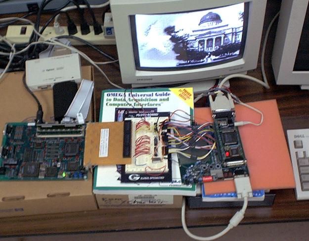
36
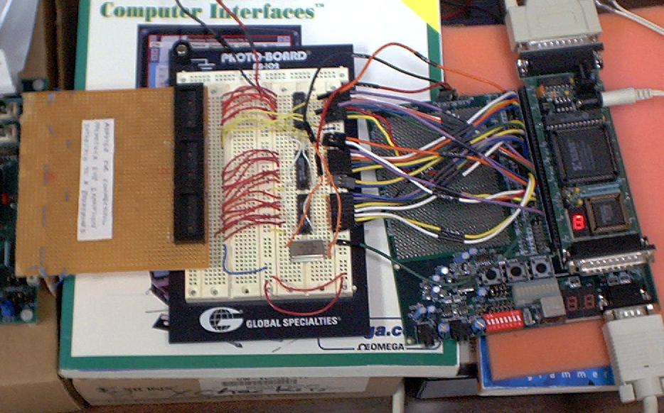
37
2608 Sweetgum Drive Apex NC Toll-free: International: FAX: How to install and use your new XStend Board
 2608 Sweetgum Drive Apex NC 27502 Toll-free: 800-549-9377 International: 919-387-0076 FAX: 919-387-1302 XStend Board V1.3 Manual How to install and use your new XStend Board RELEASE DATE: 7/5/1999 Copyright
Lab 3: VGA Bouncing Ball I
 CpE 487 Digital Design Lab Lab 3: VGA Bouncing Ball I 1. Introduction In this lab, we will program the FPGA on the Nexys2 board to display a bouncing ball on a 640 x 480 VGA monitor connected to the VGA
Design and Implementation of SOC VGA Controller Using Spartan-3E FPGA
 Design and Implementation of SOC VGA Controller Using Spartan-3E FPGA 1 ARJUNA RAO UDATHA, 2 B.SUDHAKARA RAO, 3 SUDHAKAR.B. 1 Dept of ECE, PG Scholar, 2 Dept of ECE, Associate Professor, 3 Electronics,
Design and Implementation of an AHB VGA Peripheral
 Design and Implementation of an AHB VGA Peripheral 1 Module Overview Learn about VGA interface; Design and implement an AHB VGA peripheral; Program the peripheral using assembly; Lab Demonstration. System
FPGA Laboratory Assignment 4. Due Date: 06/11/2012
 FPGA Laboratory Assignment 4 Due Date: 06/11/2012 Aim The purpose of this lab is to help you understanding the fundamentals of designing and testing memory-based processing systems. In this lab, you will
Side Street. Traffic Sensor. Main Street. Walk Button. Traffic Lights
 6.111 Laboratory 2 1 Laboratory 2 Finite State Machines Massachusetts Institute of Technology Department of Electrical Engineering and Computer Science 6.111 - Introductory Digital Systems Laboratory Handout
IMS B007 A transputer based graphics board
 IMS B007 A transputer based graphics board INMOS Technical Note 12 Ray McConnell April 1987 72-TCH-012-01 You may not: 1. Modify the Materials or use them for any commercial purpose, or any public display,
Laboratory Exercise 7
 Laboratory Exercise 7 Finite State Machines This is an exercise in using finite state machines. Part I We wish to implement a finite state machine (FSM) that recognizes two specific sequences of applied
Using the XSV Board Xchecker Interface
 Using the XSV Board Xchecker Interface May 1, 2001 (Version 1.0) Application Note by D. Vanden Bout Summary This application note shows how to configure the XC9510 CPLD on the XSV Board to enable the programming
HDL & High Level Synthesize (EEET 2035) Laboratory II Sequential Circuits with VHDL: DFF, Counter, TFF and Timer
 Laboratory II Sequential Circuits with VHDL: DFF, Counter, TFF and Timer") 1 P a g e HDL & High Level Synthesize (EEET 2035) Laboratory II Sequential Circuits with VHDL: DFF, Counter, TFF and Timer Objectives: Develop the behavioural style VHDL code for D-Flip Flop using gated,
1 P a g e HDL & High Level Synthesize (EEET 2035) Laboratory II Sequential Circuits with VHDL: DFF, Counter, TFF and Timer Objectives: Develop the behavioural style VHDL code for D-Flip Flop using gated,
VHDL Design and Implementation of FPGA Based Logic Analyzer: Work in Progress
 VHDL Design and Implementation of FPGA Based Logic Analyzer: Work in Progress Nor Zaidi Haron Ayer Keroh +606-5552086 zaidi@utem.edu.my Masrullizam Mat Ibrahim Ayer Keroh +606-5552081 masrullizam@utem.edu.my
Lab 6: Video Game PONG
 CpE 487 Digital Design Lab Lab 6: Video Game PONG 1. Introduction In this lab, we will extend the FPGA code we developed in Labs 3 and 4 (Bouncing Ball) to build a simple version of the 1970 s arcade game
TSIU03: Lab 3 - VGA. Petter Källström, Mario Garrido. September 10, 2018
 Petter Källström, Mario Garrido September 10, 2018 Abstract In the initialization of the DE2-115 (after you restart it), an image is copied into the SRAM memory. What you have to do in this lab is to read
Digital Systems Laboratory 1 IE5 / WS 2001
 Digital Systems Laboratory 1 IE5 / WS 2001 university of applied sciences fachhochschule hamburg FACHBEREICH ELEKTROTECHNIK UND INFORMATIK digital and microprocessor systems laboratory In this course you
Block Diagram. dw*3 pixin (RGB) pixin_vsync pixin_hsync pixin_val pixin_rdy. clk_a. clk_b. h_s, h_bp, h_fp, h_disp, h_line
 pixin_vsync pixin_hsync pixin_val pixin_rdy. clk_a. clk_b. h_s, h_bp, h_fp, h_disp, h_line") Key Design Features Block Diagram Synthesizable, technology independent IP Core for FPGA, ASIC and SoC reset underflow Supplied as human readable VHDL (or Verilog) source code Simple FIFO input interface
Key Design Features Block Diagram Synthesizable, technology independent IP Core for FPGA, ASIC and SoC reset underflow Supplied as human readable VHDL (or Verilog) source code Simple FIFO input interface
Lab # 9 VGA Controller
 Lab # 9 VGA Controller Introduction VGA Controller is used to control a monitor (PC monitor) and has a simple protocol as we will see in this lab. Kit parts for this lab 1 A closer look VGA Basics The
MASSACHUSETTS INSTITUTE OF TECHNOLOGY Department of Electrical Engineering and Computer Sciences
 MASSACHUSETTS INSTITUTE OF TECHNOLOGY Department of Electrical Engineering and Computer Sciences Introductory Digital Systems Lab (6.111) Quiz #2 - Spring 2003 Prof. Anantha Chandrakasan and Prof. Don
Massachusetts Institute of Technology Department of Electrical Engineering and Computer Science Introductory Digital Systems Laboratory
 Problem Set Issued: March 2, 2007 Problem Set Due: March 14, 2007 Massachusetts Institute of Technology Department of Electrical Engineering and Computer Science 6.111 Introductory Digital Systems Laboratory
Massachusetts Institute of Technology Department of Electrical Engineering and Computer Science Introductory Digital Systems Laboratory
 Problem Set Issued: March 3, 2006 Problem Set Due: March 15, 2006 Massachusetts Institute of Technology Department of Electrical Engineering and Computer Science 6.111 Introductory Digital Systems Laboratory
Digital Blocks Semiconductor IP
 Digital Blocks Semiconductor IP General Description The Digital Blocks core is a full function equivalent to the Motorola MC6845 device. The interfaces a microprocessor to a raster-scan CRT display. The
Read-only memory (ROM) Digital logic: ALUs Sequential logic circuits. Don't cares. Bus
 Digital logic: ALUs Sequential logic circuits. Don't cares. Bus") Digital logic: ALUs Sequential logic circuits CS207, Fall 2004 October 11, 13, and 15, 2004 1 Read-only memory (ROM) A form of memory Contents fixed when circuit is created n input lines for 2 n addressable
Digital logic: ALUs Sequential logic circuits CS207, Fall 2004 October 11, 13, and 15, 2004 1 Read-only memory (ROM) A form of memory Contents fixed when circuit is created n input lines for 2 n addressable
Digital Electronics II 2016 Imperial College London Page 1 of 8
 Information for Candidates: The following notation is used in this paper: 1. Unless explicitly indicated otherwise, digital circuits are drawn with their inputs on the left and their outputs on the right.
Design of VGA Controller using VHDL for LCD Display using FPGA
 International OPEN ACCESS Journal Of Modern Engineering Research (IJMER) Design of VGA Controller using VHDL for LCD Display using FPGA Khan Huma Aftab 1, Monauwer Alam 2 1, 2 (Department of ECE, Integral
Design and implementation (in VHDL) of a VGA Display and Light Sensor to run on the Nexys4DDR board Report and Signoff due Week 6 (October 4)
 of a VGA Display and Light Sensor to run on the Nexys4DDR board Report and Signoff due Week 6 (October 4)") ECE 574: Modeling and synthesis of digital systems using Verilog and VHDL Fall Semester 2017 Design and implementation (in VHDL) of a VGA Display and Light Sensor to run on the Nexys4DDR board Report and
ECE 574: Modeling and synthesis of digital systems using Verilog and VHDL Fall Semester 2017 Design and implementation (in VHDL) of a VGA Display and Light Sensor to run on the Nexys4DDR board Report and
Laboratory Exercise 7
 Laboratory Exercise 7 Finite State Machines This is an exercise in using finite state machines. Part I We wish to implement a finite state machine (FSM) that recognizes two specific sequences of applied
Ryerson University Department of Electrical and Computer Engineering EES508 Digital Systems
 1 P a g e Ryerson University Department of Electrical and Computer Engineering EES508 Digital Systems Lab 5 - VHDL for Sequential Circuits: Implementing a customized State Machine 15 Marks ( 2 weeks) Due
STATIC RANDOM-ACCESS MEMORY
 STATIC RANDOM-ACCESS MEMORY by VITO KLAUDIO OCTOBER 10, 2015 CSC343 FALL 2015 PROF. IZIDOR GERTNER Table of contents 1. Objective... pg. 2 2. Functionality and Simulations... pg. 4 2.1 SR-LATCH... pg.
Spartan-II Development System
 2002-May-4 Introduction Dünner Kirchweg 77 32257 Bünde Germany www.trenz-electronic.de The Spartan-II Development System is designed to provide a simple yet powerful platform for FPGA development, which
MBI5050 Application Note
 MBI5050 Application Note Foreword In contrast to the conventional LED driver which uses an external PWM signal, MBI5050 uses the embedded PWM signal to control grayscale output and LED current, which makes
CS8803: Advanced Digital Design for Embedded Hardware
 CS883: Advanced Digital Design for Embedded Hardware Lecture 4: Latches, Flip-Flops, and Sequential Circuits Instructor: Sung Kyu Lim (limsk@ece.gatech.edu) Website: http://users.ece.gatech.edu/limsk/course/cs883
TV Synchronism Generation with PIC Microcontroller
 TV Synchronism Generation with PIC Microcontroller With the widespread conversion of the TV transmission and coding standards, from the early analog (NTSC, PAL, SECAM) systems to the modern digital formats
BUSES IN COMPUTER ARCHITECTURE
 BUSES IN COMPUTER ARCHITECTURE The processor, main memory, and I/O devices can be interconnected by means of a common bus whose primary function is to provide a communication path for the transfer of data.
FSM Cookbook. 1. Introduction. 2. What Functional Information Must be Modeled
 FSM Cookbook 1. Introduction Tau models describe the timing and functional information of component interfaces. Timing information specifies the delay in placing values on output signals and the timing
COE758 Xilinx ISE 9.2 Tutorial 2. Integrating ChipScope Pro into a project
 COE758 Xilinx ISE 9.2 Tutorial 2 ChipScope Overview Integrating ChipScope Pro into a project Conventional Signal Sampling Xilinx Spartan 3E FPGA JTAG 2 ChipScope Pro Signal Sampling Xilinx Spartan 3E FPGA
VID_OVERLAY. Digital Video Overlay Module Rev Key Design Features. Block Diagram. Applications. Pin-out Description
 Key Design Features Block Diagram Synthesizable, technology independent VHDL IP Core Video overlays on 24-bit RGB or YCbCr 4:4:4 video Supports all video resolutions up to 2 16 x 2 16 pixels Supports any
Laboratory Exercise 4
 Laboratory Exercise 4 Polling and Interrupts The purpose of this exercise is to learn how to send and receive data to/from I/O devices. There are two methods used to indicate whether or not data can be
EEM Digital Systems II
 ANADOLU UNIVERSITY DEPARTMENT OF ELECTRICAL AND ELECTRONICS ENGINEERING EEM 334 - Digital Systems II LAB 3 FPGA HARDWARE IMPLEMENTATION Purpose In the first experiment, four bit adder design was prepared
VGA 8-bit VGA Controller
 Summary This document provides detailed reference information with respect to the VGA Controller peripheral device. Core Reference CR0113 (v3.0) March 13, 2008 The VGA Controller provides a simple, 8-bit
ECE532 Digital System Design Title: Stereoscopic Depth Detection Using Two Cameras. Final Design Report
 ECE532 Digital System Design Title: Stereoscopic Depth Detection Using Two Cameras Group #4 Prof: Chow, Paul Student 1: Robert An Student 2: Kai Chun Chou Student 3: Mark Sikora April 10 th, 2015 Final
VGA Port. Chapter 5. Pin 5 Pin 10. Pin 1. Pin 6. Pin 11. Pin 15. DB15 VGA Connector (front view) DB15 Connector. Red (R12) Green (T12) Blue (R11)
 DB15 Connector. Red (R12) Green (T12) Blue (R11)") Chapter 5 VGA Port The Spartan-3 Starter Kit board includes a VGA display port and DB15 connector, indicated as 5 in Figure 1-2. Connect this port directly to most PC monitors or flat-panel LCD displays
Chapter 5 VGA Port The Spartan-3 Starter Kit board includes a VGA display port and DB15 connector, indicated as 5 in Figure 1-2. Connect this port directly to most PC monitors or flat-panel LCD displays
SignalTap Plus System Analyzer
 SignalTap Plus System Analyzer June 2000, ver. 1 Data Sheet Features Simultaneous internal programmable logic device (PLD) and external (board-level) logic analysis 32-channel external logic analyzer 166
University of California at Berkeley College of Engineering Department of Electrical Engineering and Computer Science
 University of California at Berkeley College of Engineering Department of Electrical Engineering and Computer Science EECS 150 Fall 2000 Original Lab By: J.Wawrzynek and N. Weaver Later revisions by R.
82C55A CHMOS PROGRAMMABLE PERIPHERAL INTERFACE
 Y Y Y Y Y 82C55A CHMOS PROGRAMMABLE PERIPHERAL INTERFACE Compatible with all Intel and Most Other Microprocessors High Speed Zero Wait State Operation with 8 MHz 8086 88 and 80186 188 24 Programmable I
Experiment # 4 Counters and Logic Analyzer
 EE20L - Introduction to Digital Circuits Experiment # 4. Synopsis: Experiment # 4 Counters and Logic Analyzer In this lab we will build an up-counter and a down-counter using 74LS76A - Flip Flops. The
PROCESSOR BASED TIMING SIGNAL GENERATOR FOR RADAR AND SENSOR APPLICATIONS
 PROCESSOR BASED TIMING SIGNAL GENERATOR FOR RADAR AND SENSOR APPLICATIONS Application Note ABSTRACT... 3 KEYWORDS... 3 I. INTRODUCTION... 4 II. TIMING SIGNALS USAGE AND APPLICATION... 5 III. FEATURES AND
Spartan-II Development System
 2002-May-4 Introduction Dünner Kirchweg 77 32257 Bünde Germany www.trenz-electronic.de The Spartan-II Development System is designed to provide a simple yet powerful platform for FPGA development, which
University of California at Berkeley College of Engineering Department of Electrical Engineering and Computer Science. EECS 150 Spring 2000
 University of California at Berkeley College of Engineering Department of Electrical Engineering and Computer Science EECS 150 Spring 2000 Lab 2 Finite State Machine 1 Objectives You will enter and debug
Flip-flop and Registers
 ECE 322 Digital Design with VHDL Flip-flop and Registers Lecture Textbook References n Sequential Logic Review Stephen Brown and Zvonko Vranesic, Fundamentals of Digital Logic with VHDL Design, 2 nd or
VGA Controller. Leif Andersen, Daniel Blakemore, Jon Parker University of Utah December 19, VGA Controller Components
 VGA Controller Leif Andersen, Daniel Blakemore, Jon Parker University of Utah December 19, 2012 Fig. 1. VGA Controller Components 1 VGA Controller Leif Andersen, Daniel Blakemore, Jon Parker University
Logic Analysis Basics
 Logic Analysis Basics September 27, 2006 presented by: Alex Dickson Copyright 2003 Agilent Technologies, Inc. Introduction If you have ever asked yourself these questions: What is a logic analyzer? What
Logic Analysis Basics
 Logic Analysis Basics September 27, 2006 presented by: Alex Dickson Copyright 2003 Agilent Technologies, Inc. Introduction If you have ever asked yourself these questions: What is a logic analyzer? What
Using the XC9500/XL/XV JTAG Boundary Scan Interface
 Application Note: XC95/XL/XV Family XAPP69 (v3.) December, 22 R Using the XC95/XL/XV JTAG Boundary Scan Interface Summary This application note explains the XC95 /XL/XV Boundary Scan interface and demonstrates
TV Character Generator
 TV Character Generator TV CHARACTER GENERATOR There are many ways to show the results of a microcontroller process in a visual manner, ranging from very simple and cheap, such as lighting an LED, to much
FPGA Design. Part I - Hardware Components. Thomas Lenzi
 FPGA Design Part I - Hardware Components Thomas Lenzi Approach We believe that having knowledge of the hardware components that compose an FPGA allow for better firmware design. Being able to visualise
March 13, :36 vra80334_appe Sheet number 1 Page number 893 black. appendix. Commercial Devices
 March 13, 2007 14:36 vra80334_appe Sheet number 1 Page number 893 black appendix E Commercial Devices In Chapter 3 we described the three main types of programmable logic devices (PLDs): simple PLDs, complex
... User Guide - Revision /23/04. H Happ Controls. Copyright 2003, UltraCade Technologies UVC User Guide 1/23/2004
 H Happ Controls 106 Garlisch Drive Elk Grove, IL 60007 Tel: 888-289-4277 / 847-593-6130 Fax: 847-593-6137 wwwhappcontrolscom User Guide - Revision 201 01/23/04 Copyright 2003, UltraCade Technologies UVC
2.6 Reset Design Strategy
 2.6 Reset esign Strategy Many design issues must be considered before choosing a reset strategy for an ASIC design, such as whether to use synchronous or asynchronous resets, will every flipflop receive
Entry Level Tool II. Reference Manual. System Level Solutions, Inc. (USA) Murphy Avenue San Martin, CA (408) Version : 1.0.
 Murphy Avenue San Martin, CA (408) Version : 1.0.") Entry Level Tool II Reference Manual, Inc. (USA) 14100 Murphy Avenue San Martin, CA 95046 (408) 852-0067 http://www.slscorp.com Version : 1.0.3 Date : October 7, 2005 Copyright 2005-2006,, Inc. (SLS) All
Entry Level Tool II Reference Manual, Inc. (USA) 14100 Murphy Avenue San Martin, CA 95046 (408) 852-0067 http://www.slscorp.com Version : 1.0.3 Date : October 7, 2005 Copyright 2005-2006,, Inc. (SLS) All
Reconfigurable Architectures. Greg Stitt ECE Department University of Florida
 Reconfigurable Architectures Greg Stitt ECE Department University of Florida How can hardware be reconfigurable? Problem: Can t change fabricated chip ASICs are fixed Solution: Create components that can
Lab 4: Hex Calculator
 CpE 487 Digital Design Lab Lab 4: Hex Calculator 1. Introduction In this lab, we will program the FPGA on the Nexys2 board to function as a simple hexadecimal calculator capable of adding and subtracting
Feedback Sequential Circuits
 Feedback Sequential Circuits sequential circuit output depends on 1. current inputs 2. past sequence of inputs current state feedback sequential circuit uses ordinary gates and feedback loops to create
Level and edge-sensitive behaviour
 Level and edge-sensitive behaviour Asynchronous set/reset is level-sensitive Include set/reset in sensitivity list Put level-sensitive behaviour first: process (clock, reset) is begin if reset = '0' then
Digilent Nexys-3 Cellular RAM Controller Reference Design Overview
 Digilent Nexys-3 Cellular RAM Controller Reference Design Overview General Overview This document describes a reference design of the Cellular RAM (or PSRAM Pseudo Static RAM) controller for the Digilent
Tutorial 11 ChipscopePro, ISE 10.1 and Xilinx Simulator on the Digilent Spartan-3E board
 Tutorial 11 ChipscopePro, ISE 10.1 and Xilinx Simulator on the Digilent Spartan-3E board Introduction This lab will be an introduction on how to use ChipScope for the verification of the designs done on
DEDICATED TO EMBEDDED SOLUTIONS
 DEDICATED TO EMBEDDED SOLUTIONS DESIGN SAFE FPGA INTERNAL CLOCK DOMAIN CROSSINGS ESPEN TALLAKSEN DATA RESPONS SCOPE Clock domain crossings (CDC) is probably the worst source for serious FPGA-bugs that
Overview of BDM nc. The IEEE JTAG specification is also recommended reading for those unfamiliar with JTAG. 1.2 Overview of BDM Before the intr
 Application Note AN2387/D Rev. 0, 11/2002 MPC8xx Using BDM and JTAG Robert McEwan NCSD Applications East Kilbride, Scotland As the technical complexity of microprocessors has increased, so too has the
110 MHz 256-Word Color Palette 15-, 16-, and 24-Bit True Color Power-Down RAMDAC
 110 MHz 256-Word Color Palette 15-, 16-, and 24-Bit True Color Power-Down RAMDAC Designed specifically for high-performance color graphics, the RAM- DAC supports three true-color modes: 15-bit (5:5:5,
AD9884A Evaluation Kit Documentation
 a (centimeters) AD9884A Evaluation Kit Documentation Includes Documentation for: - AD9884A Evaluation Board - SXGA Panel Driver Board Rev 0 1/4/2000 Evaluation Board Documentation For the AD9884A Purpose
CSCB58 - Lab 4. Prelab /3 Part I (in-lab) /1 Part II (in-lab) /1 Part III (in-lab) /2 TOTAL /8
 /1 Part II (in-lab) /1 Part III (in-lab) /2 TOTAL /8") CSCB58 - Lab 4 Clocks and Counters Learning Objectives The purpose of this lab is to learn how to create counters and to be able to control when operations occur when the actual clock rate is much faster.
CSCB58 - Lab 4 Clocks and Counters Learning Objectives The purpose of this lab is to learn how to create counters and to be able to control when operations occur when the actual clock rate is much faster.
VGA Pixel Buffer Stephen Just
 VGA Pixel Buffer Stephen Just 2016-02-20 1 Introduction Video output is often a useful addition to interactive projects but typically there have been many performance limitations with respect to video
Configuring the Élan SC300 Device s Internal CGA Controller for a Specific LCD Panel
 Configuring the Élan SC300 Device s Internal CGA Controller for a Specific LCD Panel Application Note This application note explains how to determine if a specific LCD panel is supported by the Élan TM
Laboratory 1 - Introduction to Digital Electronics and Lab Equipment (Logic Analyzers, Digital Oscilloscope, and FPGA-based Labkit)
") Massachusetts Institute of Technology Department of Electrical Engineering and Computer Science 6. - Introductory Digital Systems Laboratory (Spring 006) Laboratory - Introduction to Digital Electronics
Massachusetts Institute of Technology Department of Electrical Engineering and Computer Science 6. - Introductory Digital Systems Laboratory (Spring 006) Laboratory - Introduction to Digital Electronics
Report on 4-bit Counter design Report- 1, 2. Report on D- Flipflop. Course project for ECE533
 Report on 4-bit Counter design Report- 1, 2. Report on D- Flipflop Course project for ECE533 I. Objective: REPORT-I The objective of this project is to design a 4-bit counter and implement it into a chip
University Program Design Laboratory Package
 University Program Design Laboratory Package November 1999, ver. 1.02 User Guide Introduction The University Program Design Laboratory Package was designed to meet the needs of universities teaching digital
16 Stage Bi-Directional LED Sequencer
 16 Stage Bi-Directional LED Sequencer The bi-directional sequencer uses a 4 bit binary up/down counter (CD4516) and two "1 of 8 line decoders" (74HC138 or 74HCT138) to generate the popular "Night Rider"
hochschule fu r angewandte wissenschaften hamburg Prof. Dr. B. Schwarz FB Elektrotechnik/Informatik
 8 Shift Registers A Johnson counter contains the basic structure of a shift register which is made up by a chain of D- FFs. Beginning with the LSB of a register (a number of D-FFs) each D-FF output can
California State University, Bakersfield Computer & Electrical Engineering & Computer Science ECE 3220: Digital Design with VHDL Laboratory 7
 California State University, Bakersfield Computer & Electrical Engineering & Computer Science ECE 322: Digital Design with VHDL Laboratory 7 Rational: The purpose of this lab is to become familiar in using
16 Universe LED Matrix Panels Instructions
 Congratulations on buying the high performance LED matrix controller. Eight matrix LED panels 16x32 (8 to 1 scan) Four/Two LED panels 32x32 or 32x64 (16 to 1 scan) Full 24 bit color for 16 million colors,
Laboratory 9 Digital Circuits: Flip Flops, One-Shot, Shift Register, Ripple Counter
 page 1 of 5 Digital Circuits: Flip Flops, One-Shot, Shift Register, Ripple Counter Introduction In this lab, you will learn about the behavior of the D flip-flop, by employing it in 3 classic circuits:
L11/12: Reconfigurable Logic Architectures
 L11/12: Reconfigurable Logic Architectures Acknowledgements: Materials in this lecture are courtesy of the following people and used with permission. - Randy H. Katz (University of California, Berkeley,
LAX_x Logic Analyzer
 Legacy documentation LAX_x Logic Analyzer Summary This core reference describes how to place and use a Logic Analyzer instrument in an FPGA design. Core Reference CR0103 (v2.0) March 17, 2008 The LAX_x
Interfacing the TLC5510 Analog-to-Digital Converter to the
 Application Brief SLAA070 - April 2000 Interfacing the TLC5510 Analog-to-Digital Converter to the TMS320C203 DSP Perry Miller Mixed Signal Products ABSTRACT This application report is a summary of the
Point System (for instructor and TA use only)
") EEL 4744C - Drs. George and Gugel Spring Semester 2002 Final Exam NAME SS# Closed book and closed notes examination to be done in pencil. Calculators are permitted. All work and solutions are to be written
EEL 4744C - Drs. George and Gugel Spring Semester 2002 Final Exam NAME SS# Closed book and closed notes examination to be done in pencil. Calculators are permitted. All work and solutions are to be written
Counter/timer 2 of the 83C552 microcontroller
 INTODUCTION TO THE 83C552 The 83C552 is an 80C51 derivative with several extended features: 8k OM, 256 bytes AM, 10-bit A/D converter, two PWM channels, two serial I/O channels, six 8-bit I/O ports, and
EE178 Lecture Module 4. Eric Crabill SJSU / Xilinx Fall 2005
 EE178 Lecture Module 4 Eric Crabill SJSU / Xilinx Fall 2005 Lecture #9 Agenda Considerations for synchronizing signals. Clocks. Resets. Considerations for asynchronous inputs. Methods for crossing clock
Decade Counters Mod-5 counter: Decade Counter:
 Decade Counters We can design a decade counter using cascade of mod-5 and mod-2 counters. Mod-2 counter is just a single flip-flop with the two stable states as 0 and 1. Mod-5 counter: A typical mod-5
INTERLACE CHARACTER EDITOR (ICE) Programmed by Bobby Clark. Version 1.0 for the ABBUC Software Contest 2011
 Programmed by Bobby Clark. Version 1.0 for the ABBUC Software Contest 2011") INTERLACE CHARACTER EDITOR (ICE) Programmed by Bobby Clark Version 1.0 for the ABBUC Software Contest 2011 INTRODUCTION Interlace Character Editor (ICE) is a collection of three font editors written in
INTERLACE CHARACTER EDITOR (ICE) Programmed by Bobby Clark Version 1.0 for the ABBUC Software Contest 2011 INTRODUCTION Interlace Character Editor (ICE) is a collection of three font editors written in
Vending Machine. Keywords FSM, Vending Machine, FPGA, VHDL
 Vending Machine Khodur Dbouk, Basil Jajou, Kouder Abbas, Stevan Nissan Electrical and Computer Engineering Department School of Engineering and Computer Science Oakland University, Rochester, MI kdbouk@oakland.edu,
Memec Spartan-II LC User s Guide
 Memec LC User s Guide July 21, 2003 Version 1.0 1 Table of Contents Overview... 4 LC Development Board... 4 LC Development Board Block Diagram... 6 Device... 6 Clock Generation... 7 User Interfaces...
ECE337 Lab 4 Introduction to State Machines in VHDL
 ECE337 Lab Introduction to State Machines in VHDL In this lab you will: Design, code, and test the functionality of the source version of a Moore model state machine of a sliding window average filter.
EDA385 Bomberman. Fredrik Ahlberg Adam Johansson Magnus Hultin
 EDA385 Bomberman Fredrik Ahlberg ael09fah@student.lu.se Adam Johansson rys08ajo@student.lu.se Magnus Hultin ael08mhu@student.lu.se 2013-09-23 Abstract This report describes how a Super Nintendo Entertainment
Lecture 14: Computer Peripherals
 Lecture 14: Computer Peripherals The last homework and lab for the course will involve using programmable logic to make interesting things happen on a computer monitor should be even more fun than the
EECS150 - Digital Design Lecture 12 - Video Interfacing. Recap and Outline
 EECS150 - Digital Design Lecture 12 - Video Interfacing Oct. 8, 2013 Prof. Ronald Fearing Electrical Engineering and Computer Sciences University of California, Berkeley (slides courtesy of Prof. John
Debugging of VHDL Hardware Designs on Altera s DE2 Boards
 Debugging of VHDL Hardware Designs on Altera s DE2 Boards This tutorial presents some basic debugging concepts that can be helpful in creating VHDL designs for implementation on Altera s DE2 boards. It
Figure 1 Block diagram of a 4-bit binary counter
 Lab 3: Four-Bit Binary Counter EE-459/500 HDL Based Digital Design with Programmable Logic Electrical Engineering Department, University at Buffalo Last update: Cristinel Ababei, August 2012 1. Objective
Step 1 - shaft decoder to generate clockwise/anticlockwise signals
 Workshop Two Shaft Position Encoder Introduction Some industrial automation applications require control systems which know the rotational position of a shaft. Similar devices are also used for digital
Microcontrollers and Interfacing week 7 exercises
 SERIL TO PRLLEL CONVERSION Serial to parallel conversion Microcontrollers and Interfacing week exercises Using many LEs (e.g., several seven-segment displays or bar graphs) is difficult, because only a
EN2911X: Reconfigurable Computing Topic 01: Programmable Logic. Prof. Sherief Reda School of Engineering, Brown University Fall 2014
 EN2911X: Reconfigurable Computing Topic 01: Programmable Logic Prof. Sherief Reda School of Engineering, Brown University Fall 2014 1 Contents 1. Architecture of modern FPGAs Programmable interconnect
Lecture 6: Simple and Complex Programmable Logic Devices. EE 3610 Digital Systems
 EE 3610: Digital Systems 1 Lecture 6: Simple and Complex Programmable Logic Devices MEMORY 2 Volatile: need electrical power Nonvolatile: magnetic disk, retains its stored information after the removal
Hitachi Europe Ltd. ISSUE : app084/1.0 APPLICATION NOTE DATE : 28/04/99
 APPLICATION NOTE DATE : 28/04/99 Design Considerations when using a Hitachi Medium Resolution Dot Matrix Graphics LCD Introduction Hitachi produces a wide range of monochrome medium resolution dot matrix