Lecture 12: Clock and Synchronization. TIE Logic Synthesis Arto Perttula Tampere University of Technology Spring 2018
|
|
|
- Thomasine Melton
- 5 years ago
- Views:
Transcription


1 Lecture 12: Clock and Synchronization TIE Logic Synthesis Arto Perttula Tampere University of Technology Spring 2018
2 Acknowledgements Most slides were prepared by Dr. Ari Kulmala The content of the slides are partially courtesy of Ran Ginosar Pong P. Chu C.E. Cummings, D. Mills, Synchronous Resets? Asynchronous Resets? I am so confused! How will I ever know which to use? Recommended reading: Understanding Metastability in FPGAs, white paper, Altera Corporation July 2009 D. Chen, D. Singh, J. Chromczak, D. Lewis, R. Fung, D. Neto and V. Betz, A Comprehensive Approach to Modeling, Characterizing and Optimizing for Metastability in FPGAs, ACM International Symposium on Field Programmable Gate Arrays, 2010, pp R. Ginosar, Fourteen ways to fool your synchronizer, Ninth International Symposium on Asynchronous Circuits and Systems, May 2003, pp R. Ginosar, Metastability and Synchronizers: A Tutorial, IEEE D&T Comp, Sep/Oct 2011 C.E. Cummings, D. Mills, S. Golson, Asynchoronous & Synchronous Reset Design Techniques Part Deux, SNUG Boston 2003, Rev 1.2, 38 pages 2
3 Contents Recap: Why synchronous? Clock distribution network and skew, Multiple-clock systems Metastability and synchronization failure 3
4 Introduction This lecture handles issues concerning digital systems having multiple clocks or external inputs from the environment that directly feed the digital circuit Most synchronous one-clock blocks do not have to worry about these things However, when designing real-life circuits, you have to be aware of these things Clocking errors are extremely hard to detect. You should avoid them in first place with thorough reasoning. A tricky issue: even major vendors in the business have released application notes on clock domain crossings that fail 4
5 Answer: Because it works RECAP: WHY SYNCHRONOUS 5
6 Timing of a Combinational Digital System Steady state Signal has reached a stable value Modeled by Boolean algebra Transient period Signal may fluctuate No simple model Propagation delay: time to reach the steady state Hazards: the fluctuation occurring during the transient period a) Static hazard: glitch when the signal should be stable b) Dynamic hazard: a glitch in transition Caused by multiple converging paths of an output port 6
7 E.g., static-hazard (sh=ab +bc; a=c=1) b 1->0 7
8 E.g., dynamic hazard (a=c=1, d=0), b 1->0 8
9 Syncronous Paradigm to Handle Hazards Ignore glitches in the transient period and store the data when it has stabilized In a sequential circuit Use a clock signal to sample the signal and store the stable value in a register Registers introduce new timing constraints: setup time and hold time because D changes too close to clock edge Arto Perttula 9

10 Reminder: FF Timing Specification Input must be stable: Before edge setup time After edge hold time Propagation delay is the time from clock edge to the change in output IF you provide the FF with well-behaving inputs, THEN it will behave according to this specification, ELSE no guarantees
 It s transparent when clk=0 ans slave is latched to the old value Upon clk")

11 D Flip-Flop Internals DFF can be created from two D latches connected as master-slave pair There are other choices as well First latch master uses inverted clock as enable (Perhaps internally without a separate INV) It s transparent when clk=0 ans slave is latched to the old value Upon clk edge 0->1 slave turns transparent Note that rise and fall times are not 0 If D changes near edge, new value may pass through the master latch at least partially, and intermediate voltage level goes to transparent slave and something comes out This leads to DFF setup and hold constraints Arto Perttula

12 Redrawn Ball Metaphor for DFF Outcome is obvious if D does not change near clock edge Outcome is obvious if ball is not dropped accurately on the middle of the hill top Adapted from [Understanding Metastability in FPGAs, white paper, Altera Corporation July 2009] 12
13 Reminder: Defining Minimum Clock Period Clock signal is connected only to flip-flops and not to basic gates Flip-flops are the start and end point of critical path All flip-flops within one clock domain have the same clock signal (same frequency) Critical path Use the longest path delay to calculate the frequency 1. Starts from DFF s Q output 2. Passes through combinatorial logic 3. Ends to DFF s D input 4. Does not ever go through a DFF Input CLK 13 D Q State
14 Reminder: Defining Minimum Clock Period Clock signal is connected only to flip-flops and not to basic gates Flip-flops are the start and end point of critical path All flip-flops withing one clock domain have the same clock signal (same frequency) Ensure that t clk_priod t crit.path Analyze all paths Q D and use the longest path delay to calculate the frequency Critical path 1. Starts from DFF s Q output 2. Passes through combinatorial logic 3. Ends to DFF s D input 4. Does not ever go through a DFF Input CLK 14 D Q State


15 Reminder: Critical Path Components t crit. path = t p,dff + t comb + t su, dff Note that flip-flop s hold time is not part of the critical path Paths starting or ending at IO pin may be unconstrained
16 The FO4 Delay Path delays of certain logic function can be measured in FO4 delays: (Roughly) the same value expected for all technologies, e.g., 10 FO4 Compare with equivalent gate (2NAND) as size metric FO4: Delay of a gate driving Fan-Out of 4x its own size Often measured for inverter driving 4 inverters that are identical to itself Approximately FO4 = 500 ps/um * Lgate where Lgate means the length of the transistor channel in micrometers [Ho, Future of wires, 01] About 14 ps for 28 nm technology Example has a delay of a 24 FO4 and clock period at least 24+9=33 x FO t CQ =3 t SU =
17 Clk skew and finite rise/fall speeds will likely limit clk period to 10 FO4 [Ho, 01] High-end CPU is state-of-the-art. A system-on-chip (SoC) has typically much lower frequency (more FO4s in critical path).
18 CLOCK DISTRIBUTION NETWORK AND SKEW 18
 Must balance the length of clock signal wire a) FPGA: pre-fabricated clock distribution network. Easy to use. b) ASIC: Clock tree. Implementation needs attention.")
19 Clock Distribution Network Ideal clock: clock s rising edge arrive at FFs at the same time Real implementation: Driving capability of each cell is limited Need a network of buffers to drive all FFs (more effort and power) Must balance the length of clock signal wire a) FPGA: pre-fabricated clock distribution network. Easy to use. b) ASIC: Clock tree. Implementation needs attention. [Averill, IBM,99] 19
20 Clock Skew Skew: time difference between two arriving clock edges In figure, clock arrives later to flip-flop 2 20
21 Skew Affects Timing Analysis 1. Setup time constraint (impact on maximum clock rate) 2. Hold time constraint (impact on minimum combinational delay) One gets easier due to skew, and the other gets harder Note that clk signal can also be driven from bottom to top, and the following analysis example Arto Perttula would change accordingly 21
22 Example when clk2 comes after clk1 T skew = clock skew T cq = DFF clock-to-q T next = comb. delay T hold = DFF hold time T setup = DFF setup time Requirements: T cq +T next(min) > T hold + T skew T cq +T next(max) < T c T setup + T skew In general, we must assume ±T skew Larger skew could violate the hold time of dff
23 Clock Skew Clock skew normally has negative impact on synchronous sequential circuit Regarding either setup or hold constraints 1. Effect on setup time constraint: must increase clock period => lower clock frequency 2. Effect on hold time constraint: may violate hold time when D changes too fast after clock edge Can only be fixed during physical synthesis: re-route clock; re-place register and combinational logic; add artificial delay logic Rule of thumb: Skew within 10% of clock period tolerable 23
24 MULTIPLE-CLOCK SYSTEM 24


25 Synchronous (Single Clock Domain) SoC Global Clock should arrive simultaneously to all modules! This guarantees that data can be safely communicated from one IP to another. Clock tree balancing and buffering is not trivial (but doable in circuits so far). 25

 needs special attention.")
26 SoC with Multiple Clock Domains Sometimes different domains may physically overlap -- Especially in FPGA Communication between domains (e.g. data[31:0]) needs special attention. Within one domain there is no problem. 26
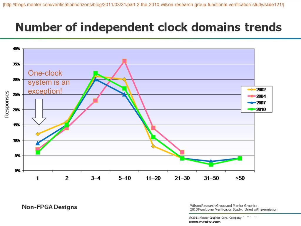
27 Why Multiple Clocks 1. Inherent multiple clock sources E.g., external communication links require their own frequencies 2. Circuit size Clock skew increases with the number of FFs in a system 3. Design complexity E.g., as system with 16-bit 20 MHz processor, 1-bit 100 MHz serial interface, 1 MHz I/O controller a) No need to optimize them all to run at 100 MHz (simpler + cheaper) b) No need to run everything at 1 MHz (better performance) 4. Power consideration Dynamic power proportional to switching frequency Use lowest frequency allowed for each IP Especially useful when combined with lowered voltage! 27
28
29 Derived vs. Independent Clocks a) Independent clocks: Relationship between clocks is unknown b) Derived clocks: A clock is derived from another clock signal (e.g., different clock rate or phase) Relationship is known Typical implementation is done with clocks that are integer multiples of each other E.g., 200 MHz bus and 800 MHz processor Logic for the derived clock should be separated from regular logic and manually synthesized (e.g., special delay line or PLL) A system with derived clock can still be treated and analyzed as a synchronous system 29

30 GALS Globally Asynchronous, Locally Synchronous system Partition a system into multiple independent subsystem with different clock domains Design and verify subsystem in same clock domain as a synchronous system Design special interface between clock domains Can be handled with the interconnection between subsystems Relaxes generation of global clock tree Nios II processor core Nios To HIBI Avalon Boot ROM NiosII External interface Data RAM Video encoding application Main control Wireless communication CPU CPU CPU CPU CPU CPU CPU Accl. CPU CPU CPU CPU CPU HIBI Segment HIBI Segment CPU Security module AES HIBI BRIDGE HIBI BRIDGE HIBI Segment CPU HIBI BRIDGE HIBI BRIDGE CPU CPU HIBI Segment CPU HIBI Segment CPU CPU CPU CPU User Interface Displ. Re-usable multiprocessor sub-systems 30

31 Taxonomy of Multiple Clock Domains 31
32 META-STABILITY AND SYNCHRONIZATION FAILURE 32
33 Timing Analysis of a Synchronous System To satisfy setup time constraint: a) Signal from a register Controlled by clock Adjust clock period to avoid setup time violation Adjust routing to avoid hold time violation b) Signal from external input Same as a) if the external input comes from another synchronous subsystem Otherwise, have to deal with the occurence of setup and hold time violation 33
34 Asynchronous Input Button press D Q clk We have no clue when the button is pressed, i.e., we cannot guarantee that it will adhere to the setup constraints Setup/hold time violations inevitably occur 34
35 Asynchronous Input (2) Button press D Q D Q clk Signal arrives to flip-flops at slightly different times due to routing delays In the example, the button s rising edge arrives to upper DFF just before clock edge, and just after it to the lower one On the next cycle, also the lower DFF captures it OK HOWEVER, a state machine may have gone awry already! E.g., one-hot state machine leaves one state but does not enter any other state, i.e., zero-hot, or it is in two states simultaneously, or it may Something needs to be done 35

36 Asynchronous Input (3) Button press 0,0 meta 1 D Q D Q D Q 0,0, ,0,0 0 1 clk Output of first DFF goes metastable at some point The following DFF s fo not necessarily interpret it the same way! Upper one thinks value is 1 Lower one thinks it is 0 This is why it is so hard to measure: logic gates and analyzer tool might interpret it differently Logic analyzer s probe will also cause some load which changes behaviour a little 36
37 Two Asynchronous Clock Domains Comb D Q D Q clk1 clk2 clk1 frequency ~33 MHz (30 ns period) clk2 frequency 62.5 MHz (16 ns period) t setup, t hold = 0.1 ns The clk2 DFF setup/hold time violations inevitably occur Event in D2 is too close to rising edge of clk2 Similar to previous case 37
38 Asynchronous Failures 38


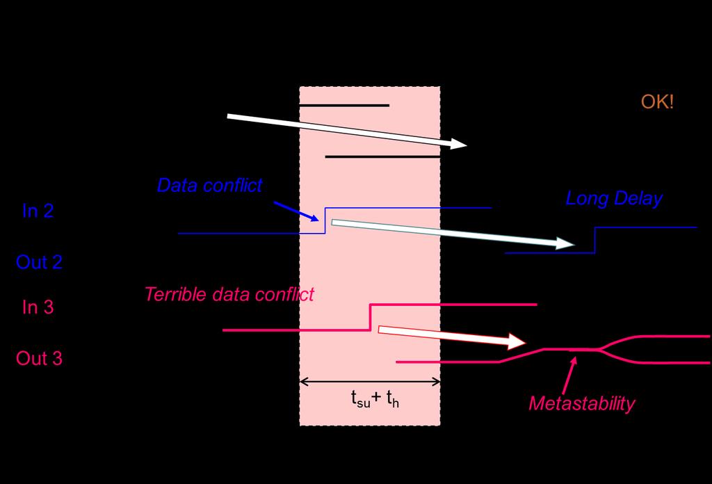
39 Main Effect of Setup Violation 39

40 Long Delay / Metastability due to Data Conflicts
41 Metastability Is Hard to Detect MTBF can be several months. Most of the time everything works and then something does not How to reproduce that? Basic RTL simulation cannot notice metastability! May be captured at accurate gate-level simulation DFF s are instantiated as components and they have checking mechanisms Too tedious and slow to be feasible Logic analyzers connected to real chip cannot detect metastability well The metastable signal values (somewhere between 0 and 1) are assumed either 0 or 1 Logic analyzer may interpret them differently than real logic Slow path might be detected if one uses very high sampling frequency Synchronizers must be tested separately and on real HW Automatically send large amounts of known values and check all Note! Absence of evidence is not evidence of absence. However, already a single error shows that the synchronizer is broken. 41
42 What Happens after Failure? a) Output of FF becomes 1 (sampled old input value) b) Output of FF becomes 0 (sampled new input value) c) FF enters metastable state, the output exhibits an in-between value FF eventually resolves to one of stable states Sometimes it is claimed that FF starts to oscillate, but that is very rare in CMOS technology (i.e., in the mainstream technology) The resolution time is a random variable with distribution function τ is a decay time constant Determined by electrical characteristics of the FF Typically today a fraction of a nanosecond The propability that metastability persists beyond Tr (i.e., cannot be resolved within Tr) P(T r) Arto Perttula T r
43 MTBF(T r ) Synchronization failure: An FF cannot resolve the metastable condition within the given time MTBF Mean Time Between (here: synchronization) Failures Basic criterion for metastability analysis Frequently expressed as a function of T r T r is the time allowed for the FF to recover some state (0/1) after a metastable event Note that then there is T r less time for the combinatorial logic (Tr affects T CQ, i.e., it is in critical path) 43
44 MTBF computation f clk = FF clock frequency f d = Data input change rate ω = susceptible time window Propability that the flip flop does not resolve within T r τ is a DFF s decay time constant Average number of synchronization failures in second Mean time between (synch.) failures Arto Perttula 44
45 E.g. 0.13m technology, danger window ω =66ps, decay constant =33 ps, f clk =200MHz, input change rate f d =0.1f clk Note that the examples in the course book are valid but for much older technology R.Ginosar s guesstimate, See references Tr [ns] MTBF Column sec hours days years E+04 years E+06 years E+09 years E+12 years E+14 years E+17 years E+19 years E+22 years E+25 years E+27 years E+30 years Age of Earth ~10 10 years 45
46 Xilinx FPGA Real-Life CLB Flip-Flops, Virtex II Pro (0.13u, 1.5Vcc) 46
47 NOTE: Figures for CPLDs, quite old technology 47 =T r
48 MTBF with Multiple DFFs 1/MTBF = λ = failure rate of the component E.g., MTBF = 100 years, failure rate of 1% per year The shown MTBF calculation is for one DFF only For multiple DFFs, error-free behaviour means that none of DFFs misbehaves MTBF(s) = 1/(1/MTBF(s 0 )+1/MTBF(s 1 )+ +1/MTBF(s n )) where MTBF(s n )= MTBF of synchronizer i E.g., MTBF(s 0 ) = 1000 years and MTBF(s 1 ) = 500 years, then MTBF(s) = 333 years E.g., MTBF(s 0 ) = 1000 years, having 20 of them reduces MTBF to 1/(20*1/1000) = 1000/20 = 50 years 48
49 Observations MTBF is statistical average, not a guarantee Large calculated MTBF gives you some confidence but, however, may not give the correct result in reality Parameters ω and depend on implementation technology Only T r can be adjusted in practical design Slack time for the FF, before the value is required to be stable, can be increased => lower frequency MTBF is extremenly sensitive to Tr Tr is in the exponent of MTBF equation Small variation in Tr can lead to large swing in MTBF Good: synchronization failure can be easily avoided by providing additional resolution time Bad: minor modification can introduce synchronization failure 49
50 Observations (2) Incorrect assumption: MTBF is 100 years, everything s fine MTBF should be thinked over the whole amount of chips If chips are sold with this design, then /100 devices fail every year 2.7 per day you are out of the business! MTBF should always be calculated Remember that there are other components that might fail also E.g., memories and logic due to radiation For reliable figures, one mus obtain the ω and values of the used technology Metastability Basically an analog phenomena Resolution time is not exact but probability function Resolved value is random Cannot be easily modeled or simulated in gate level (only X ) Cannot be easily observed or measured in physical circuit (e.g., logic analyzer might not recognize and possibly long MTBF = 3 month/chip) 50

51 Estimating MTBF via Measurement Sample the synchronizer output Q d on both rising and falling edge of clock Qf samples first - after half a cycle - and then Qr samples after full cycle If values differ, Qd was very probably metastable at the halfway of the cycle Cannot detect metastability that resolves fast, i.e., Tr<Tcycle/2 Perhaps using multiple phase-shifted clocks for sampling would detect also these Arto Perttula 51
52 Timing Example clkb is faster here Qs is simplest test signal Just toggles on every clka cycle, i.e., divides it s frequency by 2 Orange star indicates when Qs changes too close to clkb Hold time violation Qd goes metastable Resolves to 1 within cycle Lower DFF samples Qd first Qd is metastable value and Qf stays 0 here Upper DFF samples the resolved value of Qd correctly (Qr=1) xor output rises always when Qf!= Qr Error is detected only when xor output is 0 at falling edge of clkb (blue star) 52
53 Conclusions Asynchronous inputs to synchronous system violate FFs timing constraints FFs go metastable MTBF/#chips must be on range of > 10 4 years at least in order to call design safe 53
Lecture 13: Clock and Synchronization. TIE Logic Synthesis Arto Perttula Tampere University of Technology Spring 2017
 Lecture 13: Clock and Synchronization TIE-50206 Logic Synthesis Arto Perttula Tampere University of Technology Spring 2017 Acknowledgements Most slides were prepared by Dr. Ari Kulmala The content of the
TKT-1212 Digitaalijärjestelmien toteutus. Lecture 13 - Clock and Synchronization Erno Salminen, Spring 2013
 TKT-1212 Digitaalijärjestelmien toteutus Lecture 13 - Clock and Synchronization Erno Salminen, Spring 2013 Acknowledgements Most slides were prepared by Dr. Ari Kulmala The content of the slides are partially
EE178 Spring 2018 Lecture Module 5. Eric Crabill
 EE178 Spring 2018 Lecture Module 5 Eric Crabill Goals Considerations for synchronizing signals Clocks Resets Considerations for asynchronous inputs Methods for crossing clock domains Clocks The academic
https://daffy1108.wordpress.com/2014/06/08/synchronizers-for-asynchronous-signals/
 https://daffy1108.wordpress.com/2014/06/08/synchronizers-for-asynchronous-signals/ Synchronizers for Asynchronous Signals Asynchronous signals causes the big issue with clock domains, namely metastability.
EITF35: Introduction to Structured VLSI Design
 EITF35: Introduction to Structured VLSI Design Part 4.2.1: Learn More Liang Liu liang.liu@eit.lth.se 1 Outline Crossing clock domain Reset, synchronous or asynchronous? 2 Why two DFFs? 3 Crossing clock
DEDICATED TO EMBEDDED SOLUTIONS
 DEDICATED TO EMBEDDED SOLUTIONS DESIGN SAFE FPGA INTERNAL CLOCK DOMAIN CROSSINGS ESPEN TALLAKSEN DATA RESPONS SCOPE Clock domain crossings (CDC) is probably the worst source for serious FPGA-bugs that
Clock Domain Crossing. Presented by Abramov B. 1
 Clock Domain Crossing Presented by Abramov B. 1 Register Transfer Logic Logic R E G I S T E R Transfer Logic R E G I S T E R Presented by Abramov B. 2 RTL (cont) An RTL circuit is a digital circuit composed
11. Sequential Elements
 11. Sequential Elements Jacob Abraham Department of Electrical and Computer Engineering The University of Texas at Austin VLSI Design Fall 2017 October 11, 2017 ECE Department, University of Texas at Austin
EE178 Lecture Module 4. Eric Crabill SJSU / Xilinx Fall 2005
 EE178 Lecture Module 4 Eric Crabill SJSU / Xilinx Fall 2005 Lecture #9 Agenda Considerations for synchronizing signals. Clocks. Resets. Considerations for asynchronous inputs. Methods for crossing clock
More on Flip-Flops Digital Design and Computer Architecture: ARM Edition 2015 Chapter 3 <98> 98
 More on Flip-Flops Digital Design and Computer Architecture: ARM Edition 2015 Chapter 3 98 Review: Bit Storage SR latch S (set) Q R (reset) Level-sensitive SR latch S S1 C R R1 Q D C S R D latch Q
Combinational vs Sequential
 Combinational vs Sequential inputs X Combinational Circuits outputs Z A combinational circuit: At any time, outputs depends only on inputs Changing inputs changes outputs No regard for previous inputs
Laboratory 1 - Introduction to Digital Electronics and Lab Equipment (Logic Analyzers, Digital Oscilloscope, and FPGA-based Labkit)
") Massachusetts Institute of Technology Department of Electrical Engineering and Computer Science 6. - Introductory Digital Systems Laboratory (Spring 006) Laboratory - Introduction to Digital Electronics
Massachusetts Institute of Technology Department of Electrical Engineering and Computer Science 6. - Introductory Digital Systems Laboratory (Spring 006) Laboratory - Introduction to Digital Electronics
Software Engineering 2DA4. Slides 9: Asynchronous Sequential Circuits
 Software Engineering 2DA4 Slides 9: Asynchronous Sequential Circuits Dr. Ryan Leduc Department of Computing and Software McMaster University Material based on S. Brown and Z. Vranesic, Fundamentals of
Metastability Analysis of Synchronizer
 Forn International Journal of Scientific Research in Computer Science and Engineering Research Paper Vol-1, Issue-3 ISSN: 2320 7639 Metastability Analysis of Synchronizer Ankush S. Patharkar *1 and V.
2.6 Reset Design Strategy
 2.6 Reset esign Strategy Many design issues must be considered before choosing a reset strategy for an ASIC design, such as whether to use synchronous or asynchronous resets, will every flipflop receive
Figure 1 shows a simple implementation of a clock switch, using an AND-OR type multiplexer logic.
 1. CLOCK MUXING: With more and more multi-frequency clocks being used in today's chips, especially in the communications field, it is often necessary to switch the source of a clock line while the chip
FPGA TechNote: Asynchronous signals and Metastability
 FPGA TechNote: Asynchronous signals and Metastability This Doulos FPGA TechNote gives a brief overview of metastability as it applies to the design of FPGAs. The first section introduces metastability
ECE 555 DESIGN PROJECT Introduction and Phase 1
 March 15, 1998 ECE 555 DESIGN PROJECT Introduction and Phase 1 Charles R. Kime Dept. of Electrical and Computer Engineering University of Wisconsin Madison Phase I Due Wednesday, March 24; One Week Grace
6.S084 Tutorial Problems L05 Sequential Circuits
 Preamble: Sequential Logic Timing 6.S084 Tutorial Problems L05 Sequential Circuits In Lecture 5 we saw that for D flip-flops to work correctly, the flip-flop s input should be stable around the rising
Asynchronous inputs. 9 - Metastability and Clock Recovery. A simple synchronizer. Only one synchronizer per input
 9 - Metastability and Clock Recovery Asynchronous inputs We will consider a number of issues related to asynchronous inputs, multiple clock domains, clock synchronisation and clock distribution. Useful
cascading flip-flops for proper operation clock skew Hardware description languages and sequential logic
 equential logic equential circuits simple circuits with feedback latches edge-triggered flip-flops Timing methodologies cascading flip-flops for proper operation clock skew Basic registers shift registers
EECS150 - Digital Design Lecture 10 - Interfacing. Recap and Topics
 EECS150 - Digital Design Lecture 10 - Interfacing Oct. 1, 2013 Prof. Ronald Fearing Electrical Engineering and Computer Sciences University of California, Berkeley (slides courtesy of Prof. John Wawrzynek)
Clock - key to synchronous systems. Lecture 7. Clocking Strategies in VLSI Systems. Latch vs Flip-Flop. Clock for timing synchronization
 Clock - key to synchronous systems Lecture 7 Clocking Strategies in VLSI Systems Peter Cheung Department of Electrical & Electronic Engineering Imperial College London Clocks help the design of FSM where
Clock - key to synchronous systems. Topic 7. Clocking Strategies in VLSI Systems. Latch vs Flip-Flop. Clock for timing synchronization
 Clock - key to synchronous systems Topic 7 Clocking Strategies in VLSI Systems Peter Cheung Department of Electrical & Electronic Engineering Imperial College London Clocks help the design of FSM where
Synchronous Sequential Design
 Synchronous Sequential Design SMD098 Computation Structures Lecture 4 1 Synchronous sequential systems Almost all digital systems have some concept of state the outputs of a system depends on the past
NH 67, Karur Trichy Highways, Puliyur C.F, Karur District UNIT-III SEQUENTIAL CIRCUITS
 NH 67, Karur Trichy Highways, Puliyur C.F, 639 114 Karur District DEPARTMENT OF ELETRONICS AND COMMUNICATION ENGINEERING COURSE NOTES SUBJECT: DIGITAL ELECTRONICS CLASS: II YEAR ECE SUBJECT CODE: EC2203
CPS311 Lecture: Sequential Circuits
 CPS311 Lecture: Sequential Circuits Last revised August 4, 2015 Objectives: 1. To introduce asynchronous and synchronous flip-flops (latches and pulsetriggered, plus asynchronous preset/clear) 2. To introduce
1. What does the signal for a static-zero hazard look like?
 Sample Problems 1. What does the signal for a static-zero hazard look like? The signal will always be logic zero except when the hazard occurs which will cause it to temporarly go to logic one (i.e. glitch
Unit 11. Latches and Flip-Flops
 Unit 11 Latches and Flip-Flops 1 Combinational Circuits A combinational circuit consists of logic gates whose outputs, at any time, are determined by combining the values of the inputs. For n input variables,
Sequential Circuit Design: Principle
 Sequential Circuit Design: Principle modified by L.Aamodt 1 Outline 1. 2. 3. 4. 5. 6. 7. 8. Overview on sequential circuits Synchronous circuits Danger of synthesizing asynchronous circuit Inference of
CSE115: Digital Design Lecture 23: Latches & Flip-Flops
 Faculty of Engineering CSE115: Digital Design Lecture 23: Latches & Flip-Flops Sections 7.1-7.2 Suggested Reading A Generic Digital Processor Building Blocks for Digital Architectures INPUT - OUTPUT Interconnect:
Timing Error Detection: An Adaptive Scheme To Combat Variability EE241 Final Report Nathan Narevsky and Richard Ott {nnarevsky,
 Timing Error Detection: An Adaptive Scheme To Combat Variability EE241 Final Report Nathan Narevsky and Richard Ott {nnarevsky, tomott}@berkeley.edu Abstract With the reduction of feature sizes, more sources
Basis of sequential circuits: the R-S latch
 equential logic Asynchronous sequential logic state changes occur whenever state inputs change (elements may be simple wires or delay elements) ynchronous sequential logic state changes occur in lock step
Lecture 8: Sequential Logic
 Lecture 8: Sequential Logic Last lecture discussed how we can use digital electronics to do combinatorial logic we designed circuits that gave an immediate output when presented with a given set of inputs
TKK S ASIC-PIIRIEN SUUNNITTELU
 Design TKK S-88.134 ASIC-PIIRIEN SUUNNITTELU Design Flow 3.2.2005 RTL Design 10.2.2005 Implementation 7.4.2005 Contents 1. Terminology 2. RTL to Parts flow 3. Logic synthesis 4. Static Timing Analysis
System IC Design: Timing Issues and DFT. Hung-Chih Chiang
 System IC esign: Timing Issues and FT Hung-Chih Chiang Outline SoC Timing Issues Timing terminologies Synchronous vs. asynchronous design Interfaces and timing closure Clocking issues Reset esign for Testability
ELEN Electronique numérique
 ELEN0040 - Electronique numérique Patricia ROUSSEAUX Année académique 2014-2015 CHAPITRE 5 Sequential circuits design - Timing issues ELEN0040 5-228 1 Sequential circuits design 1.1 General procedure 1.2
Prototyping an ASIC with FPGAs. By Rafey Mahmud, FAE at Synplicity.
 Prototyping an ASIC with FPGAs By Rafey Mahmud, FAE at Synplicity. With increased capacity of FPGAs and readily available off-the-shelf prototyping boards sporting multiple FPGAs, it has become feasible
EECS150 - Digital Design Lecture 19 - Finite State Machines Revisited
 EECS150 - Digital Design Lecture 19 - Finite State Machines Revisited April 2, 2013 John Wawrzynek Spring 2013 EECS150 - Lec19-fsm Page 1 Finite State Machines (FSMs) FSM circuits are a type of sequential
Digital System Design
 Digital System Design by Dr. Lesley Shannon Email: lshannon@ensc.sfu.ca Course Website: http://www.ensc.sfu.ca/~lshannon/courses/ensc350 Simon Fraser University Slide Set: 8 Date: February 9, 2009 Timing
CS8803: Advanced Digital Design for Embedded Hardware
 CS883: Advanced Digital Design for Embedded Hardware Lecture 4: Latches, Flip-Flops, and Sequential Circuits Instructor: Sung Kyu Lim (limsk@ece.gatech.edu) Website: http://users.ece.gatech.edu/limsk/course/cs883
EECS150 - Digital Design Lecture 18 - Circuit Timing (2) In General...
 In General...") EECS150 - Digital Design Lecture 18 - Circuit Timing (2) March 17, 2010 John Wawrzynek Spring 2010 EECS150 - Lec18-timing(2) Page 1 In General... For correct operation: T τ clk Q + τ CL + τ setup for all
EECS150 - Digital Design Lecture 18 - Circuit Timing (2) March 17, 2010 John Wawrzynek Spring 2010 EECS150 - Lec18-timing(2) Page 1 In General... For correct operation: T τ clk Q + τ CL + τ setup for all
Design for Testability
 TDTS 01 Lecture 9 Design for Testability Zebo Peng Embedded Systems Laboratory IDA, Linköping University Lecture 9 The test problems Fault modeling Design for testability techniques Zebo Peng, IDA, LiTH
EL302 DIGITAL INTEGRATED CIRCUITS LAB #3 CMOS EDGE TRIGGERED D FLIP-FLOP. Due İLKER KALYONCU, 10043
 EL302 DIGITAL INTEGRATED CIRCUITS LAB #3 CMOS EDGE TRIGGERED D FLIP-FLOP Due 16.05. İLKER KALYONCU, 10043 1. INTRODUCTION: In this project we are going to design a CMOS positive edge triggered master-slave
Sequencing. Lan-Da Van ( 范倫達 ), Ph. D. Department of Computer Science National Chiao Tung University Taiwan, R.O.C. Fall,
, Ph. D. Department of Computer Science National Chiao Tung University Taiwan, R.O.C. Fall,") Sequencing ( 范倫達 ), Ph. D. Department of Computer Science National Chiao Tung University Taiwan, R.O.C. Fall, 2013 ldvan@cs.nctu.edu.tw http://www.cs.nctu.edu.tw/~ldvan/ Outlines Introduction Sequencing
Sequencing ( 范倫達 ), Ph. D. Department of Computer Science National Chiao Tung University Taiwan, R.O.C. Fall, 2013 ldvan@cs.nctu.edu.tw http://www.cs.nctu.edu.tw/~ldvan/ Outlines Introduction Sequencing
Digital Logic & Computer Design CS Professor Dan Moldovan Spring Chapter 3 :: Sequential Logic Design
 igital Logic & Computer esign CS 4341 Professor an Moldovan Spring 21 Copyright 27 Elsevier 3- Chapter 3 :: Sequential Logic esign igital esign and Computer Architecture avid Money Harris and Sarah
DIGITAL SYSTEM FUNDAMENTALS (ECE421) DIGITAL ELECTRONICS FUNDAMENTAL (ECE422) LATCHES and FLIP-FLOPS
 DIGITAL ELECTRONICS FUNDAMENTAL (ECE422) LATCHES and FLIP-FLOPS") COURSE / CODE DIGITAL SYSTEM FUNDAMENTALS (ECE421) DIGITAL ELECTRONICS FUNDAMENTAL (ECE422) LATCHES and FLIP-FLOPS In the same way that logic gates are the building blocks of combinatorial circuits, latches
COURSE / CODE DIGITAL SYSTEM FUNDAMENTALS (ECE421) DIGITAL ELECTRONICS FUNDAMENTAL (ECE422) LATCHES and FLIP-FLOPS In the same way that logic gates are the building blocks of combinatorial circuits, latches
ECE321 Electronics I
 ECE321 Electronics I Lecture 25: Sequential Logic: Flip-flop Payman Zarkesh-Ha Office: ECE Bldg. 230B Office hours: Tuesday 2:00-3:00PM or by appointment E-mail: pzarkesh.unm.edu Slide: 1 Review of Last
Synchronization in Asynchronously Communicating Digital Systems
 Synchronization in Asynchronously Communicating Digital Systems Priyadharshini Shanmugasundaram Abstract Two digital systems working in different clock domains require a protocol to communicate with each
ECEN454 Digital Integrated Circuit Design. Sequential Circuits. Sequencing. Output depends on current inputs
 ECEN454 igital Integrated Circuit esign Sequential Circuits ECEN 454 Combinational logic Sequencing Output depends on current inputs Sequential logic Output depends on current and previous inputs Requires
Lecture 21: Sequential Circuits. Review: Timing Definitions
 Lecture 21: Sequential Circuits Setup and Hold time MS FF Power PC Pulsed FF HLFF, SFF, SAFF Source: Ch 7 J. Rabaey notes, Weste and Harris Notes Review: Timing efinitions T C : Propagation elay from Ck
The basic logic gates are the inverter (or NOT gate), the AND gate, the OR gate and the exclusive-or gate (XOR). If you put an inverter in front of
, the AND gate, the OR gate and the exclusive-or gate (XOR). If you put an inverter in front of") 1 The basic logic gates are the inverter (or NOT gate), the AND gate, the OR gate and the exclusive-or gate (XOR). If you put an inverter in front of the AND gate, you get the NAND gate etc. 2 One of the
1 The basic logic gates are the inverter (or NOT gate), the AND gate, the OR gate and the exclusive-or gate (XOR). If you put an inverter in front of the AND gate, you get the NAND gate etc. 2 One of the
Scan. This is a sample of the first 15 pages of the Scan chapter.
 Scan This is a sample of the first 15 pages of the Scan chapter. Note: The book is NOT Pinted in color. Objectives: This section provides: An overview of Scan An introduction to Test Sequences and Test
Lecture 10: Sequential Circuits
 Introduction to CMOS VLSI esign Lecture 10: Sequential Circuits avid Harris Harvey Mudd College Spring 2004 1 Outline Floorplanning Sequencing Sequencing Element esign Max and Min-elay Clock Skew Time
Level and edge-sensitive behaviour
 Level and edge-sensitive behaviour Asynchronous set/reset is level-sensitive Include set/reset in sensitivity list Put level-sensitive behaviour first: process (clock, reset) is begin if reset = '0' then
Modeling Latches and Flip-flops
 Lab Workbook Introduction Sequential circuits are digital circuits in which the output depends not only on the present input (like combinatorial circuits), but also on the past sequence of inputs. In effect,
Slide Set 7. for ENEL 353 Fall Steve Norman, PhD, PEng. Electrical & Computer Engineering Schulich School of Engineering University of Calgary
 Slide Set 7 for ENEL 353 Fall 216 Steve Norman, PhD, PEng Electrical & Computer Engineering Schulich School of Engineering University of Calgary Fall Term, 216 SN s ENEL 353 Fall 216 Slide Set 7 slide
L4: Sequential Building Blocks (Flip-flops, Latches and Registers)
") L4: Sequential Building Blocks (Flip-flops, Latches and Registers) Acknowledgements: Lecture material adapted from R. Katz, G. Borriello, Contemporary Logic esign (second edition), Prentice-Hall/Pearson
L4: Sequential Building Blocks (Flip-flops, Latches and Registers) Acknowledgements: Lecture material adapted from R. Katz, G. Borriello, Contemporary Logic esign (second edition), Prentice-Hall/Pearson
Lec 24 Sequential Logic Revisited Sequential Circuit Design and Timing
 Traversing igital esign EECS - Components and esign Techniques for igital Systems EECS wks 6 - Lec 24 Sequential Logic Revisited Sequential Circuit esign and Timing avid Culler Electrical Engineering and
Chapter 6. sequential logic design. This is the beginning of the second part of this course, sequential logic.
 Chapter 6. sequential logic design This is the beginning of the second part of this course, sequential logic. 1 equential logic equential circuits simple circuits with feedback latches edge-triggered flip-flops
FPGA Laboratory Assignment 4. Due Date: 06/11/2012
 FPGA Laboratory Assignment 4 Due Date: 06/11/2012 Aim The purpose of this lab is to help you understanding the fundamentals of designing and testing memory-based processing systems. In this lab, you will
Objectives. Combinational logics Sequential logics Finite state machine Arithmetic circuits Datapath
 Objectives Combinational logics Sequential logics Finite state machine Arithmetic circuits Datapath In the previous chapters we have studied how to develop a specification from a given application, and
data and is used in digital networks and storage devices. CRC s are easy to implement in binary
 Introduction Cyclic redundancy check (CRC) is an error detecting code designed to detect changes in transmitted data and is used in digital networks and storage devices. CRC s are easy to implement in
EE292: Fundamentals of ECE
 EE292: Fundamentals of ECE Fall 2012 TTh 10:00-11:15 SEB 1242 Lecture 23 121120 http://www.ee.unlv.edu/~b1morris/ee292/ 2 Outline Review Combinatorial Logic Sequential Logic 3 Combinatorial Logic Circuits
Sequential logic. Circuits with feedback. How to control feedback? Sequential circuits. Timing methodologies. Basic registers
 equential logic equential circuits simple circuits with feedback latches edge-triggered flip-flops Timing methodologies cascading flip-flops for proper operation clock skew Basic registers shift registers
Asynchronous IC Interconnect Network Design and Implementation Using a Standard ASIC Flow
 Asynchronous IC Interconnect Network Design and Implementation Using a Standard ASIC Flow Bradley R. Quinton*, Mark R. Greenstreet, Steven J.E. Wilton*, *Dept. of Electrical and Computer Engineering, Dept.
EE 447/547 VLSI Design. Lecture 9: Sequential Circuits. VLSI Design EE 447/547 Sequential circuits 1
 EE 447/547 VLSI esign Lecture 9: Sequential Circuits Sequential circuits 1 Outline Floorplanning Sequencing Sequencing Element esign Max and Min-elay Clock Skew Time Borrowing Two-Phase Clocking Sequential
problem maximum score 1 28pts 2 10pts 3 10pts 4 15pts 5 14pts 6 12pts 7 11pts total 100pts
 University of California at Berkeley College of Engineering Department of Electrical Engineering and Computer Sciences EECS150 J. Wawrzynek Spring 2002 4/5/02 Midterm Exam II Name: Solutions ID number:
L14: Quiz Information and Final Project Kickoff. L14: Spring 2004 Introductory Digital Systems Laboratory
 L14: Quiz Information and Final Project Kickoff 1 Quiz Quiz Review on Monday, March 29 by TAs 7:30 P.M. to 9:30 P.M. Room 34-101 Quiz will be Closed Book on March 31 st (during class time, Location, Walker
Lecture #4: Clocking in Synchronous Circuits
 Lecture #4: Clocking in Synchronous Circuits Kunle Stanford EE183 January 15, 2003 Tutorial/Verilog Questions? Tutorial is done, right? Due at midnight (Fri 1/17/03) Turn in copies of all verilog, copy
Outline. EECS150 - Digital Design Lecture 27 - Asynchronous Sequential Circuits. Cross-coupled NOR gates. Asynchronous State Transition Diagram
 EECS150 - Digital Design Lecture 27 - Asynchronous Sequential Circuits Nov 26, 2002 John Wawrzynek Outline SR Latches and other storage elements Synchronizers Figures from Digital Design, John F. Wakerly
Digital Integrated Circuits EECS 312
 14 12 10 8 6 Fujitsu VP2000 IBM 3090S Pulsar 4 IBM 3090 IBM RY6 CDC Cyber 205 IBM 4381 IBM RY4 2 IBM 3081 Apache Fujitsu M380 IBM 370 Merced IBM 360 IBM 3033 Vacuum Pentium II(DSIP) 0 1950 1960 1970 1980
Introduction to Sequential Circuits
 Introduction to Sequential Circuits COE 202 Digital Logic Design Dr. Muhamed Mudawar King Fahd University of Petroleum and Minerals Presentation Outline Introduction to Sequential Circuits Synchronous
IT T35 Digital system desigm y - ii /s - iii
 UNIT - III Sequential Logic I Sequential circuits: latches flip flops analysis of clocked sequential circuits state reduction and assignments Registers and Counters: Registers shift registers ripple counters
ALGORITHMS IN HW EECS150 ALGORITHMS IN HW. COMBINATIONAL vs. SEQUENTIAL. Sequential Circuits ALGORITHMS IN HW
 LGOITHM HW EEC150 ection 2 Introduction to equential Logic Fall 2001 pproach #2: Combinational divide & conquer a[0] a[1] a[1022] a[1023] MX MX MX 512 + 256 + K+ 1 = 1023 blocks Each MX block has: 64 s;
DEPARTMENT OF ELECTRICAL &ELECTRONICS ENGINEERING DIGITAL DESIGN
 DEPARTMENT OF ELECTRICAL &ELECTRONICS ENGINEERING DIGITAL DESIGN Assoc. Prof. Dr. Burak Kelleci Spring 2018 OUTLINE Synchronous Logic Circuits Latch Flip-Flop Timing Counters Shift Register Synchronous
Product Level MTBF Calculation
 2014 Fifth International Conference on Intelligent Systems, Modelling and Simulation Product Level MTBF Calculation Ang Boon Chong easic Corp bang@easic.com Abstract Synchronizers are used in sampling
Efficient Architecture for Flexible Prescaler Using Multimodulo Prescaler
 Efficient Architecture for Flexible Using Multimodulo G SWETHA, S YUVARAJ Abstract This paper, An Efficient Architecture for Flexible Using Multimodulo is an architecture which is designed from the proposed
6. Sequential Logic Flip-Flops
 ection 6. equential Logic Flip-Flops Page of 5 6. equential Logic Flip-Flops ombinatorial components: their output values are computed entirely from their present input values. equential components: their
CMOS Implementation of Reliable Synchronizer for Multi clock domain System-on-chip
 RESEARCH ARTICLE OPEN ACCESS CMOS Implementation of Reliable Synchronizer for Multi clock domain System-on-chip Vivek khetade 1, Dr. S.S. Limaye 2 Sarang Purnaye 3 1 Department of Electronic design Technology,
EECS 270 Midterm 1 Exam Closed book portion Winter 2017
 EES 270 Midterm 1 Exam losed book portion Winter 2017 Name: unique name: Sign the honor code: I have neither given nor received aid on this exam nor observed anyone else doing so. NOTES: 1. This part of
L12: Reconfigurable Logic Architectures
 L12: Reconfigurable Logic Architectures Acknowledgements: Materials in this lecture are courtesy of the following sources and are used with permission. Frank Honore Prof. Randy Katz (Unified Microelectronics
EEC 118 Lecture #9: Sequential Logic. Rajeevan Amirtharajah University of California, Davis Jeff Parkhurst Intel Corporation
 EEC 118 Lecture #9: Sequential Logic Rajeevan Amirtharajah University of California, Davis Jeff Parkhurst Intel Corporation Outline Review: Static CMOS Logic Finish Static CMOS transient analysis Sequential
Measurements of metastability in MUTEX on an FPGA
 LETTER IEICE Electronics Express, Vol.15, No.1, 1 11 Measurements of metastability in MUTEX on an FPGA Nguyen Van Toan, Dam Minh Tung, and Jeong-Gun Lee a) E-SoC Lab/Smart Computing Lab, Dept. of Computer
Chapter 7 Memory and Programmable Logic
 EEA091 - Digital Logic 數位邏輯 Chapter 7 Memory and Programmable Logic 吳俊興國立高雄大學資訊工程學系 2006 Chapter 7 Memory and Programmable Logic 7-1 Introduction 7-2 Random-Access Memory 7-3 Memory Decoding 7-4 Error
Chapter 5: Synchronous Sequential Logic
 Chapter 5: Synchronous Sequential Logic NCNU_2016_DD_5_1 Digital systems may contain memory for storing information. Combinational circuits contains no memory elements the outputs depends only on the inputs
Testability: Lecture 23 Design for Testability (DFT) Slide 1 of 43
 Slide 1 of 43") Testability: Lecture 23 Design for Testability (DFT) Shaahin hi Hessabi Department of Computer Engineering Sharif University of Technology Adapted, with modifications, from lecture notes prepared p by
Testability: Lecture 23 Design for Testability (DFT) Shaahin hi Hessabi Department of Computer Engineering Sharif University of Technology Adapted, with modifications, from lecture notes prepared p by
Chapter 6. sequential logic design. This is the beginning of the second part of this course, sequential logic.
 Chapter 6. sequential logic design This is the beginning of the second part of this course, sequential logic. equential logic equential circuits simple circuits with feedback latches edge-triggered flip-flops
Sequential Logic. E&CE 223 Digital Circuits and Systems (A. Kennings) Page 1
 Page 1") Sequential Logic E&CE 223 igital Circuits and Systems (A. Kennings) Page 1 Sequential Circuits Have considered only combinational circuits in which circuit outputs are determined entirely by current circuit
Sequential Logic E&CE 223 igital Circuits and Systems (A. Kennings) Page 1 Sequential Circuits Have considered only combinational circuits in which circuit outputs are determined entirely by current circuit
Static Timing Analysis for Nanometer Designs
 J. Bhasker Rakesh Chadha Static Timing Analysis for Nanometer Designs A Practical Approach 4y Spri ringer Contents Preface xv CHAPTER 1: Introduction / 1.1 Nanometer Designs 1 1.2 What is Static Timing
FPGA Design. Part I - Hardware Components. Thomas Lenzi
 FPGA Design Part I - Hardware Components Thomas Lenzi Approach We believe that having knowledge of the hardware components that compose an FPGA allow for better firmware design. Being able to visualise
Lecture 11: Sequential Circuit Design
 Lecture 11: Sequential Circuit esign Outline q Sequencing q Sequencing Element esign q Max and Min-elay q Clock Skew q Time Borrowing q Two-Phase Clocking 2 Sequencing q Combinational logic output depends
Chapter 5 Flip-Flops and Related Devices
 Chapter 5 Flip-Flops and Related Devices Chapter 5 Objectives Selected areas covered in this chapter: Constructing/analyzing operation of latch flip-flops made from NAND or NOR gates. Differences of synchronous/asynchronous
INTEGRATED CIRCUITS. AN219 A metastability primer Nov 15
 INTEGRATED CIRCUITS 1989 Nov 15 INTRODUCTION When using a latch or flip-flop in normal circumstances (i.e., when the device s setup and hold times are not being violated), the outputs will respond to a
Sequential Circuits: Latches & Flip-Flops
 Sequential Circuits: Latches & Flip-Flops Overview Storage Elements Latches SR, JK, D, and T Characteristic Tables, Characteristic Equations, Eecution Tables, and State Diagrams Standard Symbols Flip-Flops
Notes on Digital Circuits
 PHYS 331: Junior Physics Laboratory I Notes on Digital Circuits Digital circuits are collections of devices that perform logical operations on two logical states, represented by voltage levels. Standard
Switching Circuits & Logic Design
 Switching Circuits & Logic Design Jie-Hong oland Jiang 江介宏 Department of Electrical Engineering National Taiwan University Fall 22 Latches and Flip-Flops http://www3.niaid.nih.gov/topics/malaria/lifecycle.htm
Software Engineering 2DA4. Slides 3: Optimized Implementation of Logic Functions
 Software Engineering 2DA4 Slides 3: Optimized Implementation of Logic Functions Dr. Ryan Leduc Department of Computing and Software McMaster University Material based on S. Brown and Z. Vranesic, Fundamentals
Introduction. NAND Gate Latch. Digital Logic Design 1 FLIP-FLOP. Digital Logic Design 1
 2007 Introduction BK TP.HCM FLIP-FLOP So far we have seen Combinational Logic The output(s) depends only on the current values of the input variables Here we will look at Sequential Logic circuits The
FSM Implementations. TIE Logic Synthesis Arto Perttula Tampere University of Technology Fall Output. Input. Next. State.
 FSM Implementations TIE-50206 Logic Synthesis Arto Perttula Tampere University of Technology Fall 2016 Input Next State Current state Output Moore Acknowledgements Prof. Pong P. Chu provided official slides