Lecture 21: Sequential Circuits. Review: Timing Definitions
|
|
|
- Christal Hubbard
- 5 years ago
- Views:
Transcription
1 Lecture 21: Sequential Circuits Setup and Hold time MS FF Power PC Pulsed FF HLFF, SFF, SAFF Source: Ch 7 J. Rabaey notes, Weste and Harris Notes Review: Timing efinitions T C : Propagation elay from Ck to, assuming has been set early enough relative to Ck T setup (U): minimum time between change and the transparency Ck Edge, such that will be guaranteed to change T hold : minimum time must be held after the triggering Clk edge T skew : spatial variation of clock arrival time between two points in the chip t t su ATA STABLE t hold t Register t c 2 q ATA STABLE t 1


2 FF/Latch esign Balancing act Power, area, speed Look for similarities in FF/Latch design Input stage X Internal Node output stage ata Storage Internal Node Stores sampled data. How? Static: stores as long as power is on ynamic: store data in a capacitor (internal node capacitance) 2
3 Sampling How do you sample data? Sampling should occur for =Hi and =Lo Consider the following Latches Timing Issues Clk t t (a) Clk- elay t T Clk- 1.05t C 2 t C 2 t Su t 2 C t H T Setup-1 (b) T Hold-1 -CK delay Time 3
4 elay vs. Setup/Hold times Ck- (ps) t setup t hold X Clk -Ck (ps) Why does t CK- increase when setup/hold times are NOT met? sampling storage X Resolve time window large X Resolve time window too small Metastable Types of Flops MASTER-SLAVE FF PULSE-TRIGGERE FF data 4
5 Hard vs. Soft Clk edges Flop Latch Power PC 603 (Gerosa, JSSC 94) 5
6 Power PC 603 (Gerosa, JSSC 94 Low power feedback and low internal power High clock load More power dissipated in clock distribution network Small Ck- delay positive setup time Pay attention to: iffusion input: overshoot/undershoot due to unbuffered input Race issues due to clock skew Sequencing: Pulsed Latches How to generate short pulse? Pulsed Latches p t pw p p Latch Combinational Logic Latch 6

7 Hybrid Latch Flip-Flop AM K-6, Hamid Partovi, ISSCC 1996 Clocked transistors ata Transistors HLFF timing waveforms X 1-1 Glitch =Hi Clk_db Clk Clk_db X 7
8 Flip-Flop features HLFF Single phase clock Edge triggered (single clock edge) Latch features Transparency period (3 inv delays) Negative setup time. Absorbs skew Hold time comparable to HLFF delay Clk- delay can be smaller than hold time (verify for all process corners) Fully Static Semi-ynamic Flip-Flop (SFF) Sun UltraSparc III, Fabian Klass, JSSC 99 8
9 SFF 1 storage S S 0 1 =Hi =Lo Embed logic into latch 9
 Nice interface from domino logic Pulse generation stage is fast (resolves small input voltages) Ideal for low swing input signaling Nand RS static latch")
10 Sense-amplifier based FF (SAFF) Matsui et. al EC Alpha 21264, Strong Arm Input stage Cross-coupled inv. Pre-charge/Sampling Sense Amplifier FF (SAFF) Nice interface from domino logic Pulse generation stage is fast (resolves small input voltages) Ideal for low swing input signaling Nand RS static latch is speed bottleneck and b output waveforms are not symmetric 10
11 Master-Slave vs Pulsed-Triggered Master-Slave Positive setup time Hold-time close to zero Two clock phases required istributed globally Generated locally Hard edge property Sensitive to clock skew Pulsed-Triggered Negative setup time (data can arrive after edge) Sensitive to hold-time violation (t ck-q < t hold ) Soft edge property (absorbs clock skew) Flip-Flop Performance Comparison 11
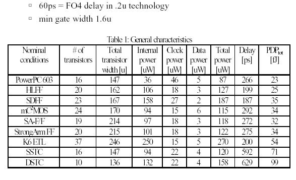
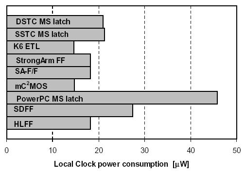
12 General Characteristics Clock Power Consumption 12
EE241 - Spring 2007 Advanced Digital Integrated Circuits. Announcements
 EE241 - Spring 2007 Advanced igital Integrated Circuits Lecture 24: Advanced Flip-Flops Synchronization Announcements Homework 5 due on 4/26 Final exam on May 8 in class Project presentations on May 3,
Lecture 26: Multipliers. Final presentations May 8, 1-5pm, BWRC Final reports due May 7 Final exam, Monday, May :30pm, 241 Cory
 EE241 - Spring 2008 Advanced Digital Integrated Circuits Lecture 26: Multipliers Latches Announcements Homework 5 Due today Wrapping-up the class: Final presentations May 8, 1-5pm, BWRC Final reports due
ECE321 Electronics I
 ECE321 Electronics I Lecture 25: Sequential Logic: Flip-flop Payman Zarkesh-Ha Office: ECE Bldg. 230B Office hours: Tuesday 2:00-3:00PM or by appointment E-mail: pzarkesh.unm.edu Slide: 1 Review of Last
Sequential Circuit Design: Part 1
 Sequential Circuit esign: Part 1 esign of memory elements Static latches Pseudo-static latches ynamic latches Timing parameters Two-phase clocking Clocked inverters James Morizio 1 Sequential Logic FFs
Sequential Circuit Design: Part 1
 Sequential ircuit esign: Part 1 esign of memory elements Static latches Pseudo-static latches ynamic latches Timing parameters Two-phase clocking locked inverters Krish hakrabarty 1 Sequential Logic FFs
Lecture 6. Clocked Elements
 Lecture 6 Clocked Elements Computer Systems Laboratory Stanford University horowitz@stanford.edu Copyright 2006 Mark Horowitz, Ron Ho Some material taken from lecture notes by Vladimir Stojanovic and Ken
ECEN454 Digital Integrated Circuit Design. Sequential Circuits. Sequencing. Output depends on current inputs
 ECEN454 igital Integrated Circuit esign Sequential Circuits ECEN 454 Combinational logic Sequencing Output depends on current inputs Sequential logic Output depends on current and previous inputs Requires
ISSCC 2003 / SESSION 19 / PROCESSOR BUILDING BLOCKS / PAPER 19.5
 ISSCC 2003 / SESSION 19 / PROCESSOR BUILDING BLOCKS / PAPER 19.5 19.5 A Clock Skew Absorbing Flip-Flop Nikola Nedovic 1,2, Vojin G. Oklobdzija 2, William W. Walker 1 1 Fujitsu Laboratories of America,
11. Sequential Elements
 11. Sequential Elements Jacob Abraham Department of Electrical and Computer Engineering The University of Texas at Austin VLSI Design Fall 2017 October 11, 2017 ECE Department, University of Texas at Austin
Lecture 11: Sequential Circuit Design
 Lecture 11: Sequential Circuit esign Outline q Sequencing q Sequencing Element esign q Max and Min-elay q Clock Skew q Time Borrowing q Two-Phase Clocking 2 Sequencing q Combinational logic output depends
L4: Sequential Building Blocks (Flip-flops, Latches and Registers)
") L4: Sequential Building Blocks (Flip-flops, Latches and Registers) Acknowledgements: Lecture material adapted from R. Katz, G. Borriello, Contemporary Logic esign (second edition), Prentice-Hall/Pearson
L4: Sequential Building Blocks (Flip-flops, Latches and Registers) Acknowledgements: Lecture material adapted from R. Katz, G. Borriello, Contemporary Logic esign (second edition), Prentice-Hall/Pearson
MASSACHUSETTS INSTITUTE OF TECHNOLOGY Department of Electrical Engineering and Computer Science
 MASSACHUSETTS INSTITUTE OF TECHNOLOGY epartment of Electrical Engineering and Computer Science 6.374: Analysis and esign of igital Integrated Circuits Problem Set # 5 Fall 2003 Issued: 10/28/03 ue: 11/12/03
EE-382M VLSI II FLIP-FLOPS
 EE-382M VLSI II FLIP-FLOPS Gian Gerosa, Intel Fall 2008 EE 382M Class Notes Page # 1 / 31 OUTLINE Trends LATCH Operation FLOP Timing Diagrams & Characterization Transfer-Gate Master-Slave FLIP-FLOP Merged
Chapter 7 Sequential Circuits
 Chapter 7 Sequential Circuits Jin-Fu Li Advanced Reliable Systems (ARES) Lab. epartment of Electrical Engineering National Central University Jungli, Taiwan Outline Latches & Registers Sequencing Timing
CPE/EE 427, CPE 527 VLSI Design I Sequential Circuits. Sequencing
 CPE/EE 427, CPE 527 VLSI esign I Sequential Circuits epartment of Electrical and Computer Engineering University of Alabama in Huntsville Aleksandar Milenkovic ( www.ece.uah.edu/~milenka ) Combinational
Topic 8. Sequential Circuits 1
 Topic 8 Sequential Circuits 1 Peter Cheung Department of Electrical & Electronic Engineering Imperial College London Rabaey Chapter 7 URL: www.ee.ic.ac.uk/pcheung/ E-mail: p.cheung@ic.ac.uk 1 Based on
A Unified Approach in the Analysis of Latches and Flip-Flops for Low-Power Systems
 A Unified Approach in the Analysis of Latches and Flip-Flops for Low-Power Systems Vladimir Stojanovic University of Belgrade, Yugoslavia Bulevar Revolucije 73.Beograd, Yugoslavia +38 3 336 sv793d@kiklop.etf.bg.ac.yu
Sequential Logic. E&CE 223 Digital Circuits and Systems (A. Kennings) Page 1
 Page 1") Sequential Logic E&CE 223 igital Circuits and Systems (A. Kennings) Page 1 Sequential Circuits Have considered only combinational circuits in which circuit outputs are determined entirely by current circuit
Sequential Logic E&CE 223 igital Circuits and Systems (A. Kennings) Page 1 Sequential Circuits Have considered only combinational circuits in which circuit outputs are determined entirely by current circuit
(CSC-3501) Lecture 7 (07 Feb 2008) Seung-Jong Park (Jay) CSC S.J. Park. Announcement
 Lecture 7 (07 Feb 2008) Seung-Jong Park (Jay) CSC S.J. Park. Announcement") Seung-Jong Park (Jay) http://www.csc.lsu.edu/~sjpark Computer Architecture (CSC-3501) Lecture 7 (07 Feb 2008) 1 Announcement 2 1 Combinational vs. Sequential Logic Combinational Logic Memoryless Outputs
Seung-Jong Park (Jay) http://www.csc.lsu.edu/~sjpark Computer Architecture (CSC-3501) Lecture 7 (07 Feb 2008) 1 Announcement 2 1 Combinational vs. Sequential Logic Combinational Logic Memoryless Outputs
EEC 118 Lecture #9: Sequential Logic. Rajeevan Amirtharajah University of California, Davis Jeff Parkhurst Intel Corporation
 EEC 118 Lecture #9: Sequential Logic Rajeevan Amirtharajah University of California, Davis Jeff Parkhurst Intel Corporation Outline Review: Static CMOS Logic Finish Static CMOS transient analysis Sequential
Basis of sequential circuits: the R-S latch
 equential logic Asynchronous sequential logic state changes occur whenever state inputs change (elements may be simple wires or delay elements) ynchronous sequential logic state changes occur in lock step
High Performance Dynamic Hybrid Flip-Flop For Pipeline Stages with Methodical Implanted Logic
 High Performance Dynamic Hybrid Flip-Flop For Pipeline Stages with Methodical Implanted Logic K.Vajida Tabasum, K.Chandra Shekhar Abstract-In this paper we introduce a new high performance dynamic hybrid
UNIT III COMBINATIONAL AND SEQUENTIAL CIRCUIT DESIGN
 UNIT III COMBINATIONAL AND SEQUENTIAL CIRCUIT DESIGN Part A (2 Marks) 1. What is a BiCMOS? BiCMOS is a type of integrated circuit that uses both bipolar and CMOS technologies. 2. What are the problems
cascading flip-flops for proper operation clock skew Hardware description languages and sequential logic
 equential logic equential circuits simple circuits with feedback latches edge-triggered flip-flops Timing methodologies cascading flip-flops for proper operation clock skew Basic registers shift registers
Energy Recovery Clocking Scheme and Flip-Flops for Ultra Low-Energy Applications
 Energy Recovery Clocking Scheme and Flip-Flops for Ultra Low-Energy Applications Matthew Cooke, Hamid Mahmoodi-Meimand, Kaushik Roy School of Electrical and Computer Engineering, Purdue University, West
Digital System Clocking: High-Performance and Low-Power Aspects
 igital ystem Clocking: High-Performance and Low-Power Aspects Vojin G. Oklobdzija, Vladimir M. tojanovic, ejan M. Markovic, Nikola M. Nedovic Chapter 8: tate-of-the-art Clocked torage Elements in CMO Technology
Memory elements. Topics. Memory element terminology. Variations in memory elements. Clock terminology. Memory element parameters. clock.
 Topics! Memory elements.! Basics of sequential machines. Memory elements! Stores a value as controlled by clock.! May have load signal, etc.! In CMOS, memory is created by:! capacitance (dynamic);! feedback
CMOS Latches and Flip-Flops
 CMOS Latches and Flip-Flops João Canas Ferreira University of Porto Faculty of Engineering 2016-05-04 Topics 1 General Aspects 2 Circuits based on positive feedback 3 Circuits based on charge storage João
The outputs are formed by a combinational logic function of the inputs to the circuit or the values stored in the flip-flops (or both).
.") 1 The outputs are formed by a combinational logic function of the inputs to the circuit or the values stored in the flip-flops (or both). The value that is stored in a flip-flop when the clock pulse occurs
1 The outputs are formed by a combinational logic function of the inputs to the circuit or the values stored in the flip-flops (or both). The value that is stored in a flip-flop when the clock pulse occurs
Memory, Latches, & Registers
 Memory, Latches, & Registers 1) Structured Logic Arrays 2) Memory Arrays 3) Transparent Latches 4) How to save a few bucks at toll booths 5) Edge-triggered Registers L13 Memory 1 General Table Lookup Synthesis
Sequencing. Lan-Da Van ( 范倫達 ), Ph. D. Department of Computer Science National Chiao Tung University Taiwan, R.O.C. Fall,
, Ph. D. Department of Computer Science National Chiao Tung University Taiwan, R.O.C. Fall,") Sequencing ( 范倫達 ), Ph. D. Department of Computer Science National Chiao Tung University Taiwan, R.O.C. Fall, 2013 ldvan@cs.nctu.edu.tw http://www.cs.nctu.edu.tw/~ldvan/ Outlines Introduction Sequencing
Sequencing ( 范倫達 ), Ph. D. Department of Computer Science National Chiao Tung University Taiwan, R.O.C. Fall, 2013 ldvan@cs.nctu.edu.tw http://www.cs.nctu.edu.tw/~ldvan/ Outlines Introduction Sequencing
Lecture 10: Sequential Circuits
 Introduction to CMOS VLSI esign Lecture 10: Sequential Circuits avid Harris Harvey Mudd College Spring 2004 1 Outline Floorplanning Sequencing Sequencing Element esign Max and Min-elay Clock Skew Time
EE 447/547 VLSI Design. Lecture 9: Sequential Circuits. VLSI Design EE 447/547 Sequential circuits 1
 EE 447/547 VLSI esign Lecture 9: Sequential Circuits Sequential circuits 1 Outline Floorplanning Sequencing Sequencing Element esign Max and Min-elay Clock Skew Time Borrowing Two-Phase Clocking Sequential
EE141-Fall 2010 Digital Integrated Circuits. Announcements. Homework #8 due next Tuesday. Project Phase 3 plan due this Sat.
 EE141-Fall 2010 Digital Integrated Circuits Lecture 24 Timing 1 1 Announcements Homework #8 due next Tuesday Project Phase 3 plan due this Sat. Hanh-Phuc s extra office hours shifted next week Tues. 3-4pm
II. ANALYSIS I. INTRODUCTION
 Characterizing Dynamic and Leakage Power Behavior in Flip-Flops R. Ramanarayanan, N. Vijaykrishnan and M. J. Irwin Dept. of Computer Science and Engineering Pennsylvania State University, PA 1682 Abstract
Engr354: Digital Logic Circuits
 Engr354: igital Circuits Chapter 7 Sequential Elements r. Curtis Nelson Sequential Elements In this chapter you will learn about: circuits that can store information; Basic cells, latches, and flip-flops;
Area Efficient Pulsed Clock Generator Using Pulsed Latch Shift Register
 International Journal for Modern Trends in Science and Technology Volume: 02, Issue No: 10, October 2016 http://www.ijmtst.com ISSN: 2455-3778 Area Efficient Pulsed Clock Generator Using Pulsed Latch Shift
Clocking Spring /18/05
 ing L06 s 1 Why s and Storage Elements? Inputs Combinational Logic Outputs Want to reuse combinational logic from cycle to cycle L06 s 2 igital Systems Timing Conventions All digital systems need a convention
Lec 24 Sequential Logic Revisited Sequential Circuit Design and Timing
 Traversing igital esign EECS - Components and esign Techniques for igital Systems EECS wks 6 - Lec 24 Sequential Logic Revisited Sequential Circuit esign and Timing avid Culler Electrical Engineering and
Unit 11. Latches and Flip-Flops
 Unit 11 Latches and Flip-Flops 1 Combinational Circuits A combinational circuit consists of logic gates whose outputs, at any time, are determined by combining the values of the inputs. For n input variables,
Glitches/hazards and how to avoid them. What to do when the state machine doesn t fit!
 State Machine Signaling Timing Behavior Glitches/hazards and how to avoid them SM Partitioning What to do when the state machine doesn t fit! State Machine Signaling Introducing Idle States (synchronous
Fundamentals of Computer Systems
 Fundamentals of Computer Systems Sequential Logic Stephen A. Edwards Columbia University Summer 2016 State-Holding Elements Bistable Elements S Latch Latch Positive-Edge-Triggered Flip-Flop Flip-Flop with
Design of a Low Power and Area Efficient Flip Flop With Embedded Logic Module
 IOSR Journal of Electronics and Communication Engineering (IOSR-JECE) e-issn: 2278-2834,p- ISSN: 2278-8735.Volume 10, Issue 6, Ver. II (Nov - Dec.2015), PP 40-50 www.iosrjournals.org Design of a Low Power
EE141-Fall 2010 Digital Integrated Circuits. Announcements. Synchronous Timing. Latch Parameters. Class Material. Homework #8 due next Tuesday
 EE-Fall 00 Digital tegrated Circuits Timing Lecture Timing Announcements Homework #8 due next Tuesday Synchronous Timing Project Phase plan due this Sat. Hanh-Phuc s extra office hours shifted next week
Homework 3 posted this week, due after Spring break Quiz #2 today Midterm project report due on Wednesday No office hour today
 EE241 - Spring 2013 Advanced Digital Integrated Circuits Lecture 14: Statistical timing Latches Announcements Homework 3 posted this week, due after Spring break Quiz #2 today Midterm project report due
INTRODUCTION TO SEQUENTIAL CIRCUITS
 NOTE: Explanation Refer Class Notes Digital Circuits(15EECC203) INTRODUCTION TO SEQUENTIAL CIRCUITS by Nagaraj Vannal, Asst.Professor, School of Electronics Engineering, K.L.E. Technological University,
Fundamentals of Computer Systems
 Fundamentals of omputer Systems Sequential Logic Martha A. Kim olumbia University Spring 2016 1/1 2/1 Bistable Elements Equivalent circuits; right is more traditional. Two stable states: 0 1 1 0 3/1 S
EL302 DIGITAL INTEGRATED CIRCUITS LAB #3 CMOS EDGE TRIGGERED D FLIP-FLOP. Due İLKER KALYONCU, 10043
 EL302 DIGITAL INTEGRATED CIRCUITS LAB #3 CMOS EDGE TRIGGERED D FLIP-FLOP Due 16.05. İLKER KALYONCU, 10043 1. INTRODUCTION: In this project we are going to design a CMOS positive edge triggered master-slave
Logic Design. Flip Flops, Registers and Counters
 Logic Design Flip Flops, Registers and Counters Introduction Combinational circuits: value of each output depends only on the values of inputs Sequential Circuits: values of outputs depend on inputs and
Combinational vs Sequential
 Combinational vs Sequential inputs X Combinational Circuits outputs Z A combinational circuit: At any time, outputs depends only on inputs Changing inputs changes outputs No regard for previous inputs
More on Flip-Flops Digital Design and Computer Architecture: ARM Edition 2015 Chapter 3 <98> 98
 More on Flip-Flops Digital Design and Computer Architecture: ARM Edition 2015 Chapter 3 98 Review: Bit Storage SR latch S (set) Q R (reset) Level-sensitive SR latch S S1 C R R1 Q D C S R D latch Q
D Latch (Transparent Latch)
") D Latch (Transparent Latch) -One way to eliminate the undesirable condition of the indeterminate state in the SR latch is to ensure that inputs S and R are never equal to 1 at the same time. This is done
D Latch (Transparent Latch) -One way to eliminate the undesirable condition of the indeterminate state in the SR latch is to ensure that inputs S and R are never equal to 1 at the same time. This is done
Figure 1 shows a simple implementation of a clock switch, using an AND-OR type multiplexer logic.
 1. CLOCK MUXING: With more and more multi-frequency clocks being used in today's chips, especially in the communications field, it is often necessary to switch the source of a clock line while the chip
A Power Efficient Flip Flop by using 90nm Technology
 A Power Efficient Flip Flop by using 90nm Technology Mrs. Y. Lavanya Associate Professor, ECE Department, Ramachandra College of Engineering, Eluru, W.G (Dt.), A.P, India. Email: lavanya.rcee@gmail.com
CHAPTER 1 LATCHES & FLIP-FLOPS
 CHAPTER 1 LATCHES & FLIP-FLOPS 1 Outcome After learning this chapter, student should be able to; Recognize the difference between latches and flipflops Analyze the operation of the flip flop Draw the output
An efficient Sense amplifier based Flip-Flop design
 An efficient Sense amplifier based Flip-Flop design Rajendra Prasad and Narayan Krishan Vyas Abstract An efficient approach for sense amplifier based flip-flop design has been introduced in this paper.
Comparative study on low-power high-performance standard-cell flip-flops
 Comparative study on low-power high-performance standard-cell flip-flops S. Tahmasbi Oskuii, A. Alvandpour Electronic Devices, Linköping University, Linköping, Sweden ABSTRACT This paper explores the energy-delay
Switching Circuits & Logic Design
 Switching Circuits & Logic Design Jie-Hong oland Jiang 江介宏 Department of Electrical Engineering National Taiwan University Fall 22 Latches and Flip-Flops http://www3.niaid.nih.gov/topics/malaria/lifecycle.htm
Synchronous Sequential Logic
 Synchronous Sequential Logic -A Sequential Circuit consists of a combinational circuit to which storage elements are connected to form a feedback path. The storage elements are devices capable of storing
Asynchronous Model of Flip-Flop s and Latches for Low Power Clocking
 Asynchronous Model of Flip-Flop s and Latches for Low Power Clocking G.Abhinaya Raja & P.Srinivas Department Of Electronics & Comm. Engineering, Nimra College of Engineering & Technology, Ibrahimpatnam,
High performance and Low power FIR Filter Design Based on Sharing Multiplication
 High performance and Low power FIR Filter esign Based on Sharing Multiplication Jongsun Park, Woopyo Jeong, Hunsoo Choo, Hamid Mahmoodi-Meimand, Yongtao Wang, Kaushik Roy School of Electrical and Computer
Chapter 11 Latches and Flip-Flops
 Chapter 11 Latches and Flip-Flops SKEE1223 igital Electronics Mun im/arif/izam FKE, Universiti Teknologi Malaysia ecember 8, 2015 Types of Logic Circuits Combinational logic: Output depends solely on the
Digital Integrated Circuits EECS 312
 14 12 10 8 6 Fujitsu VP2000 IBM 3090S Pulsar 4 IBM 3090 IBM RY6 CDC Cyber 205 IBM 4381 IBM RY4 2 IBM 3081 Apache Fujitsu M380 IBM 370 Merced IBM 360 IBM 3033 Vacuum Pentium II(DSIP) 0 1950 1960 1970 1980
Modeling and designing of Sense Amplifier based Flip-Flop using Cadence tool at 45nm
 Modeling and designing of Sense Amplifier based Flip-Flop using Cadence tool at 45nm Akhilesh Tiwari1 and Shyam Akashe2 1Research Scholar, ITM University, Gwalior, India antrixman75@gmail.com 2Associate
ECEN689: Special Topics in High-Speed Links Circuits and Systems Spring 2011
 ECEN689: Special Topics in High-Speed Links Circuits and Systems Spring 2011 Lecture 9: TX Multiplexer Circuits Sam Palermo Analog & Mixed-Signal Center Texas A&M University Announcements & Agenda Next
Hardware Design I Chap. 5 Memory elements
 Hardware Design I Chap. 5 Memory elements E-mail: shimada@is.naist.jp Why memory is required? To hold data which will be processed with designed hardware (for storage) Main memory, cache, register, and
LOW POWER AND HIGH PERFORMANCE SHIFT REGISTERS USING PULSED LATCH TECHNIQUE
 OI: 10.21917/ijme.2018.0088 LOW POWER AN HIGH PERFORMANCE SHIFT REGISTERS USING PULSE LATCH TECHNIUE Vandana Niranjan epartment of Electronics and Communication Engineering, Indira Gandhi elhi Technical
Load-Sensitive Flip-Flop Characterization
 Appears in IEEE Workshop on VLSI, Orlando, Florida, April Load-Sensitive Flip-Flop Characterization Seongmoo Heo and Krste Asanović Massachusetts Institute of Technology Laboratory for Computer Science
Digital Circuits and Systems
 Spring 2015 Week 6 Module 33 Digital Circuits and Systems Timing Sequential Circuits Shankar Balachandran* Associate Professor, CSE Department Indian Institute of Technology Madras *Currently a Visiting
Digital System Clocking: High-Performance and Low-Power Aspects. Microprocessor Examples
 igital System Clocking: High-Performance and Low-Power Aspects Vojin G. Oklobdzija, Vladimir M. Stojanovic, ejan M. Markovic, Nikola M. Nedovic Chapter 9: Microprocessor Examples Wiley-Interscience and
Timing Error Detection: An Adaptive Scheme To Combat Variability EE241 Final Report Nathan Narevsky and Richard Ott {nnarevsky,
 Timing Error Detection: An Adaptive Scheme To Combat Variability EE241 Final Report Nathan Narevsky and Richard Ott {nnarevsky, tomott}@berkeley.edu Abstract With the reduction of feature sizes, more sources
Chapter 9. Timing Design. (Based on Chapter 7 and Chapter 8 of Wakerly) Data Path Comb. Logic. Reg. Reg. Reg C <= A + B
 Data Path Comb. Logic. Reg. Reg. Reg C <= A + B") Chapter 9 Timing esign (Based on Chapter 7 and Chapter 8 of Wakerly) Timing Check X State machine Next State Logic * * 0 1 State Memory 0 1 EN Counter * 0 * Incrementer 1 0 1 A B Reg Reg ata Path Comb.
Chapter 9 Timing esign (Based on Chapter 7 and Chapter 8 of Wakerly) Timing Check X State machine Next State Logic * * 0 1 State Memory 0 1 EN Counter * 0 * Incrementer 1 0 1 A B Reg Reg ata Path Comb.
Feedback Sequential Circuits
 Feedback Sequential Circuits sequential circuit output depends on 1. current inputs 2. past sequence of inputs current state feedback sequential circuit uses ordinary gates and feedback loops to create
EMT 125 Digital Electronic Principles I CHAPTER 6 : FLIP-FLOP
 EMT 125 Digital Electronic Principles I CHAPTER 6 : FLIP-FLOP 1 Chapter Overview Latches Gated Latches Edge-triggered flip-flops Master-slave flip-flops Flip-flop operating characteristics Flip-flop applications
Digital Design, Kyung Hee Univ. Chapter 5. Synchronous Sequential Logic
 Chapter 5. Synchronous Sequential Logic 1 5.1 Introduction Electronic products: ability to send, receive, store, retrieve, and process information in binary format Dependence on past values of inputs Sequential
ELE2120 Digital Circuits and Systems. Tutorial Note 7
 ELE2120 Digital Circuits and Systems Tutorial Note 7 Outline 1. Sequential Circuit 2. Gated SR Latch 3. Gated D-latch 4. Edge-Triggered D Flip-Flop 5. Asynchronous and Synchronous reset Sequential Circuit
Project 6: Latches and flip-flops
 Project 6: Latches and flip-flops Yuan Ze University epartment of Computer Engineering and Science Copyright by Rung-Bin Lin, 1999 All rights reserved ate out: 06/5/2003 ate due: 06/25/2003 Purpose: This
AN EFFICIENT DOUBLE EDGE TRIGGERING FLIP FLOP (MDETFF)
") AN EFFICIENT DOUBLE EDGE TRIGGERING FLIP FLOP (MDETFF) S.Santhoshkumar, L.Saranya 2 (UG Scholar, Dept.of.ECE, Christ the king Engineering college, Tamilnadu, India, santhosh29ece@gmail.com) 2 (Asst. Professor,
AN EFFICIENT DOUBLE EDGE TRIGGERING FLIP FLOP (MDETFF) S.Santhoshkumar, L.Saranya 2 (UG Scholar, Dept.of.ECE, Christ the king Engineering college, Tamilnadu, India, santhosh29ece@gmail.com) 2 (Asst. Professor,
Asynchronous Data Sampling Within Clock-Gated Double Edge-Triggered Flip-Flops
 Available Online at www.ijcsmc.com International Journal of Computer Science and Mobile Computing A Monthly Journal of Computer Science and Information Technology IJCSMC, Vol. 4, Issue. 4, April 2015,
Unit 9 Latches and Flip-Flops. Dept. of Electrical and Computer Eng., NCTU 1
 Unit 9 Latches and Flip-Flops Dept. of Electrical and Computer Eng., NCTU 1 9.1 Introduction Dept. of Electrical and Computer Eng., NCTU 2 What is the characteristic of sequential circuits in contrast
Clock - key to synchronous systems. Lecture 7. Clocking Strategies in VLSI Systems. Latch vs Flip-Flop. Clock for timing synchronization
 Clock - key to synchronous systems Lecture 7 Clocking Strategies in VLSI Systems Peter Cheung Department of Electrical & Electronic Engineering Imperial College London Clocks help the design of FSM where
EEE2135 Digital Logic Design Chapter 6. Latches/Flip-Flops and Registers/Counters 서강대학교 전자공학과
 EEE235 Digital Logic Design Chapter 6. Latches/Flip-Flops and Registers/Counters 서강대학교 전자공학과 . Delay and Latches ) Signal Storage a. as voltage level static memory b. as charges dynamic memory 2) Delays
Clock - key to synchronous systems. Topic 7. Clocking Strategies in VLSI Systems. Latch vs Flip-Flop. Clock for timing synchronization
 Clock - key to synchronous systems Topic 7 Clocking Strategies in VLSI Systems Peter Cheung Department of Electrical & Electronic Engineering Imperial College London Clocks help the design of FSM where
Review of digital electronics. Storage units Sequential circuits Counters Shifters
 Review of digital electronics Storage units Sequential circuits ounters Shifters ounting in Binary A counter can form the same pattern of 0 s and 1 s with logic levels. The first stage in the counter represents
A Low-Power CMOS Flip-Flop for High Performance Processors
 A Low-Power CMOS Flip-Flop for High Performance Processors Preetisudha Meher, Kamala Kanta Mahapatra Dept. of Electronics and Telecommunication National Institute of Technology Rourkela, India Preetisudha1@gmail.com,
ECE 341. Lecture # 2
 ECE 341 Lecture # 2 Instructor: Zeshan Chishti zeshan@pdx.edu October 1, 2014 Portland State University Announcements Course website reminder: http://www.ece.pdx.edu/~zeshan/ece341.htm Homework 1: Will
System IC Design: Timing Issues and DFT. Hung-Chih Chiang
 System IC esign: Timing Issues and FT Hung-Chih Chiang Outline SoC Timing Issues Timing terminologies Synchronous vs. asynchronous design Interfaces and timing closure Clocking issues Reset esign for Testability
DESIGN OF DOUBLE PULSE TRIGGERED FLIP-FLOP BASED ON SIGNAL FEED THROUGH SCHEME
 Scientific Journal Impact Factor (SJIF): 1.711 e-issn: 2349-9745 p-issn: 2393-8161 International Journal of Modern Trends in Engineering and Research www.ijmter.com DESIGN OF DOUBLE PULSE TRIGGERED FLIP-FLOP
Sequential logic. Circuits with feedback. How to control feedback? Sequential circuits. Timing methodologies. Basic registers
 equential logic equential circuits simple circuits with feedback latches edge-triggered flip-flops Timing methodologies cascading flip-flops for proper operation clock skew Basic registers shift registers
ESE 570 STATIC SEQUENTIAL CMOS LOGIC CELLS. Kenneth R. Laker, University of Pennsylvania, updated 25Mar15
 ESE 570 STATIC SEQUENTIAL CMOS LOGIC CELLS 1 Classes of Logic Circuits two stable op. pts. Latch level triggered. Flip-Flop edge triggered. one stable op. pt. One-shot single pulse output no stable op.
SEQUENTIAL LOGIC. Sequential Logic
 EUENTIAL LOGIC equential Logic FF s LOGIC t p,comb 2 storage mechanisms positive feedback charge-based Flip-Flop: Timing efinitions t t setup thold ATA TABLE t t pff ATA TABLE t Maximum Clock Frequency
Software Engineering 2DA4. Slides 9: Asynchronous Sequential Circuits
 Software Engineering 2DA4 Slides 9: Asynchronous Sequential Circuits Dr. Ryan Leduc Department of Computing and Software McMaster University Material based on S. Brown and Z. Vranesic, Fundamentals of
Momentary Changes in Outputs. State Machine Signaling. Oscillatory Behavior. Hazards/Glitches. Types of Hazards. Static Hazards
 State Machine Signaling Momentary hanges in Outputs Timing ehavior Glitches/hazards and how to avoid them SM Partitioning What to do when the state machine doesn t fit! State Machine Signaling State Machine
Power Distribution and Clock Design
 Lecture 3 Power Distribution and Clock Design R. Saleh Dept. of ECE University of British Columbia res@ece.ubc.ca 1 Overview of Lecture Power distribution in the past was a fairly simple task Goal of power
CPS311 Lecture: Sequential Circuits
 CPS311 Lecture: Sequential Circuits Last revised August 4, 2015 Objectives: 1. To introduce asynchronous and synchronous flip-flops (latches and pulsetriggered, plus asynchronous preset/clear) 2. To introduce
Digital Integrated Circuit Design II ECE 426/526, Chapter 10 $Date: 2016/04/07 00:50:16 $
 Digital Integrated Circuit Design II ECE 426/526, Chapter 10 $Date: 2016/04/07 00:50:16 $ Professor R. Daasch Depar tment of Electrical and Computer Engineering Portland State University Portland, OR 97207-0751
Design of New Dual Edge Triggered Sense Amplifier Flip-Flop with Low Area and Power Efficient
 Design of New Dual Edge Triggered Sense Amplifier Flip-Flop with Low Area and Power Efficient Ms. Sheik Shabeena 1, R.Jyothirmai 2, P.Divya 3, P.Kusuma 4, Ch.chiranjeevi 5 1 Assistant Professor, 2,3,4,5
Energy-Delay Space Analysis for Clocked Storage Elements Under Process Variations
 Energy-Delay Space Analysis for Clocked Storage Elements Under Process Variations Christophe Giacomotto 1, Nikola Nedovic 2, and Vojin G. Oklobdzija 1 1 Advanced Computer Systems Engineering Laboratory,
Sequential Logic. References:
 Sequential Logic Reerences: Adapted rom: Digital Integrated Circuits: A Design Perspective, J. Rabaey UCB Principles o CMOS VLSI Design: A Systems Perspective, 2nd Ed., N. H. E. Weste and K. Eshraghian
EE273 Lecture 11 Pipelined Timing Closed-Loop Timing November 2, Today s Assignment
 EE273 Lecture 11 Pipelined Timing Closed-Loop Timing November 2, 1998 William J. ally Computer Systems Laboratory Stanford University billd@csl.stanford.edu Copyright (C) by William J. ally, All Rights