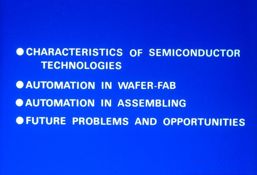
Automation in Semiconductor Manufacturing IEDM, San Francisco, 1982 Keynote Speech
|
|
|
- Maude Dean
- 5 years ago
- Views:
Transcription
1 Automation in Semiconductor Manufacturing IEDM, San Francisco, 1982 Keynote Speech Commentary Alongside ISSCC, IEDM is the most traditional academic conference in the semiconductor field, and it is held in December every year, centering on the device technology and manufacturing process. The keynote speeches are given on the first day, and it is customary for three people selected from North America, Europe, and Asia to deliver speeches. In this year, IBM in US, Siemens in Germany, and Hitachi in Japan were selected. In 1981, Japan was at the top of the world in the memory technology, and a lot of attention was gathered in Japanese manufacturing technology. I think that the turn has come around for Hitachi, since Hitachi was a leader in advanced devices of 3 micron process, such as 64K DRAM and 16K SRAM. The paper on the Technical Digest was jointly written with Hiroto Nagatomo, Manager of Production Engineering Department, and I made the presentation. It was my first experience to make a speech at a large overseas academic conference with over 2,000 audience, and it was not easy to keep talking without letting the audience get tired for an hour. It is most important that the content itself is fulfilling, but it is also necessary to incorporate some appropriate humor and to moderate the atmosphere of the venue. The first and the last slides were prepared with such intention, and I took in the taste that would invite laughter even in the middle. I wish it would help as a reference for your speech. As a result, this keynote speech was accepted very favorably. After the conference, Michael Adler, Program Chairman, sent me the following thank you note: "--- In particular, as to your speech, many people gave me comments that it was the best one in the past IEDM speeches. Not only was the content excellent, but also the presentation with humor was very well accepted. A lot of people were surprised at the depth of your understanding about American humor ---- " This is not simply a compliment to my speech, but I think that it was the high evaluation given to Japanese semiconductor technology that had reached the world's top. Continue to slides 1

2 Keynote speech at IEDM in I talked as a representative of the Asian region. It was a comprehensive speech on the automation of manufacturing advanced devices. IBM person talked on Device Technology for LSI, and Siemens person on Power Device. 2

3 I started with a slide that took the audience by surprise, and it roused the laughter and applause in the hall. "Today's story is the same as a chef's story about how delicious dishes can be made. Let me talk about various kitchen utensils and how to use them. However, the secrete treasure of traditional family seasoning is not included! 3
4 4

5 Technology in the semiconductor field has several characteristics. We must keep these points in mind prior to the implementation of automation. 5

6 Advances in semiconductor technology are extremely fast, and new waves rise with the period of about seven years. Beginning with the Ge transistor, going through Si transistors, ICs and LSIs, VLSI started to rise. VLSI will be the biggest segment in the 1990s. In promoting the automation of manufacturing, technological changes have to be taken into considerations. 6

7 Starting with 1K DRAM, and going through 4K and 16K, 64K DRAM is starting to rise. However, within the next few years the new generation 256 Kbit will surpass 64 Kbit. 7

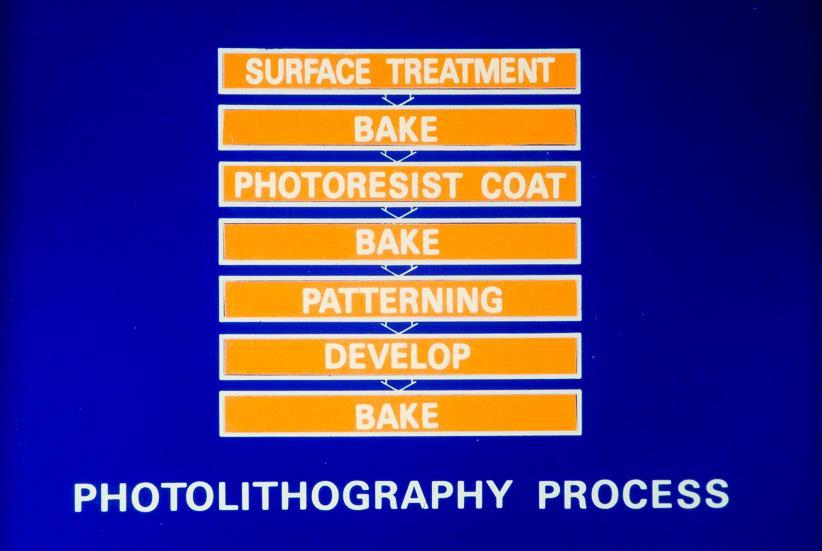
8 Although the number of bits grows rapidly, the growth in the value and quantity is moderate. This is because the cost per bit keeps falling, and the integration density keeps going up. This point has also to be considered in manufacturing automation. 8
 in 3 years,")
9 The trend of complexity, feature size, and chip area are shown from 1 K to 256 K DRAM. The integration level increases 4 times every 3 years, the pattern size is reduced to 70% (the density is doubled) in 3 years, and the chip area is doubled in 3 years. 9

10 The trend of new technologies introduced after All these technologies were "innovative" at the time of introduction. 10

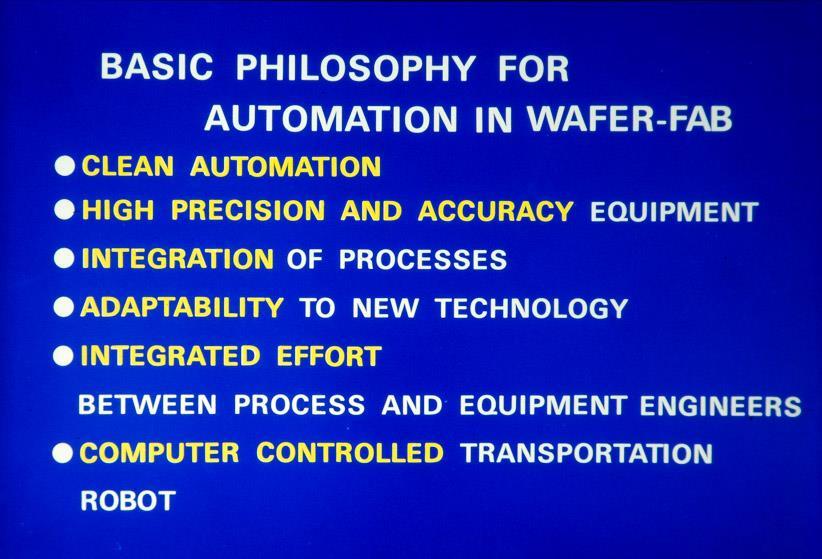
11 Actually this slide was also the one that invited big laughter in the hall. "Everyone, this shows pictures of memory cells after 16 K. It is getting smaller and smaller in every generation. The 1 Mbit cell is so small that you probably cannot see it from your seat. " 11
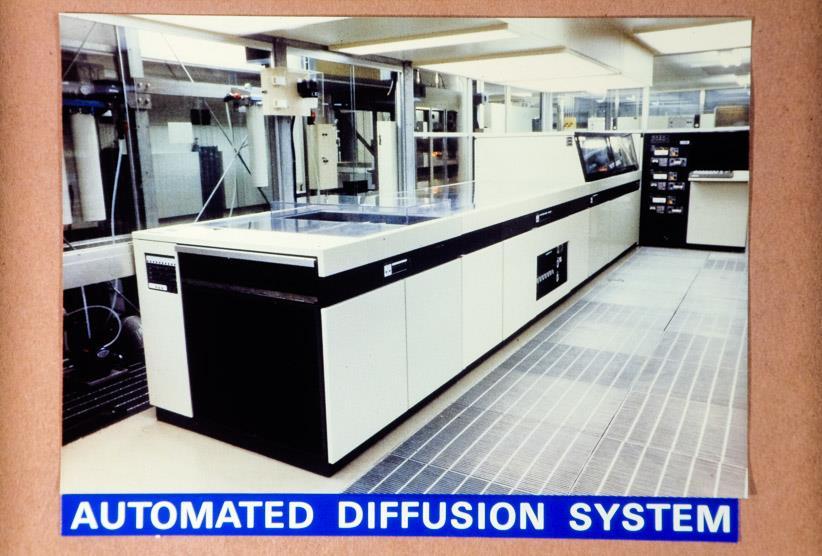
 decrease in yield, 2) decrease in throughput, 3) increase in")
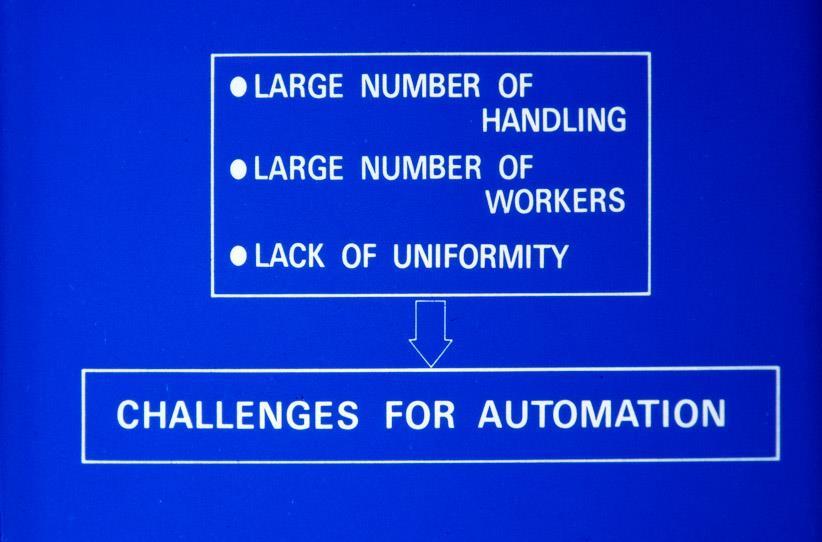
12 The following three points are challenges for automation. 1) decrease in yield, 2) decrease in throughput, 3) increase in investment amount 12

13 13
14 14
 diffusion / implantation, 2) photolithography, 3) deposition (CVD, metallization)")
15 The basis of the wafer processing is that the following three processes are repeated. 1) diffusion / implantation, 2) photolithography, 3) deposition (CVD, metallization) 15

16 16
17 17
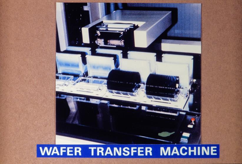
18 18

19 The wafer fab has class 1,000 clean process area in the center, and maintenance area of class 10,000 on the outside. Wafer transport between work areas is done by a computer controlled transport system. 19

20 Processing equipment are placed on the left and right side of the work area, and an automatic transfer system (robot in the middle of the right side) carries wafers between work areas. Every one, I think you are strongly impressed that there is not a single person in this automated line." After a moment of silence, "In fact, this picture was taken in the factory on a holiday. A big laughter followed. 20

21 The processes in the work zone are done by an integrated production system. 21

22 While wafers are loaded from the left side, all processes are performed during one round trip and unloaded from the left side. Through the whole process, the wafer is never touched by human hands. 22

23 23

24 No human intervention from loading to unloading. 24
25 25
26 26

27 Compared with manual work, chipping at the wafer edge is reduced to 1/10 in the case of automation. This is an example that automation contributes to quality improvement. 27

28 A robot that automatically carries wafers. While traveling on the orbit, it checks the obstacles etc. with the two eyes in front. 28

29 With the introduction of automation, manual handling decreased to 1/5 in the decade from the early 1970s to the early 1980s. 29

30 Compared with the conventional method, the productivity is improved by 1.5 times with the automated method. 30

31 This shows that the number of foreign particles on the wafer has been reduced by automation from , from month to month. 31
 in which good chips can be possibly obtained, inside the area (W) of the entire wafer, and the ratio G / W = AUF is called an area usage factor.")
32 Several slides following this are related to the yield of LSI, which was the theme which I was good at. This figure expresses the defect distribution on the wafer. There is a region (G) in which good chips can be possibly obtained, inside the area (W) of the entire wafer, and the ratio G / W = AUF is called an area usage factor. It is assumed that the defect distribution in G is Poisson distribution (stochastic distribution). 32
 increases.")
33 This is a formula used as a basis for yield analysis at the time, and even today the basic point is still valid. The yield in the region G decreases exponentially as the product of the chip area A and the defect density D (A*D) increases. The total yield Y is the product of the area usage factor AUF and the yield in the region G. 33

34 When a new product is launched, the yield is initially low, and then it improves along the learning curve. For example, in the case of a memory, it may be imaged as 1 K, 4 K, 16 K, and 64 K DRAM. 34

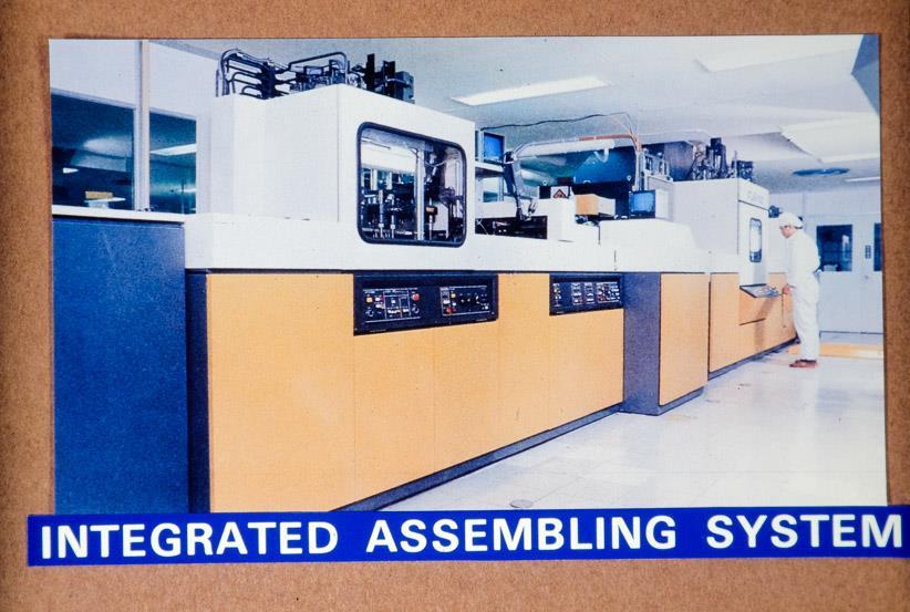
35 This shows that the defect density has been reduced by about an order of magnitude in the past 10 years. It is predicted that this trend will be accelerated further. 35

36 Types of yield improvement are classified into three typical types. A is a case where AUF is high while there are many defects in G, C is a case where there are few defects in G but AUF is low. B is in the middle. You can see the effect of improvement by plotting the path of yield improvement. It is important for all team members to share this figure because the yield improvement is often advanced by the team activities. 36

37 This shows the pace of improvement in defect density in conventional manufacturing lines and automated lines. It shows that the reduction speed of the automated line is nearly twice as fast. This material emphasizes that the effect of automation is not only labor-saving, but also the effect of quality improvement is great. 37

38 38

39 39

40 40

41 The back-end process flow is shown from the probe test to the final test. The biggest difficulty is in wire bonding process. 41

42 100 to 1,000 dies can be obtained from one wafer, and 20 to 200 wire bonds per die are necessary. That is, about 20,000 wire bonds are required for one wafer. This is a challenging task. 42
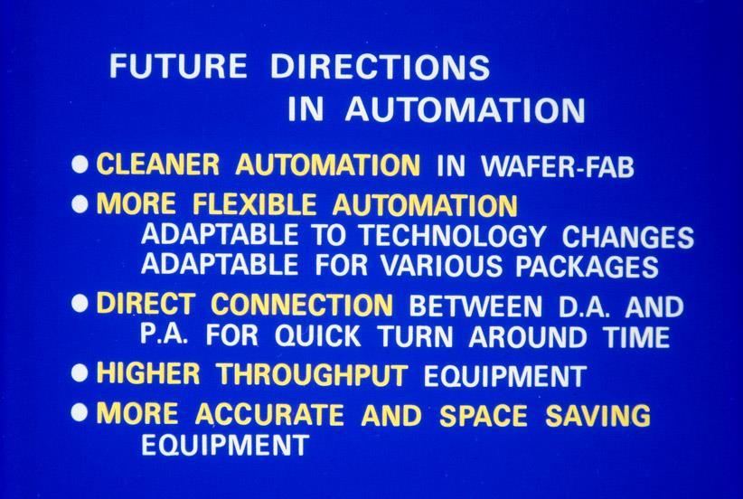
 process.")
43 The number of workers in the back-end process is about three times that of the front-end (wafer manufacturing) process. This is the challenge for automation 43
44 44

45 In 1960 s, assembling process depended on the manual work of young girls. They were called "transistor girls, and were precious as "golden eggs". It was an era when TVs and radios made by semiconductors were contributing greatly to Japan's exports. As an aside, "transistor girl" also meant a "small and cute girl", and they were very popular, too. Smiles and laughter spread in the hall. 45

46 Automation has evolved in the following steps. Manual semi-automation full-automation integrated system 46

47 Outline of integrated system is shown from supply of chips to bonding, molding, and lead-frame cutting. 47
48 48

49 This figure shows that productivity improves by orders of magnitude by the shift from manual to semi-automation, to full-automation, and to integrated assembling system. 49

50 In manual work, the bonding speed is about 1 second per wire, but for full-automation it is 0.2 sec / wire, and further improvement is expected in the integrated assembling system. 50

51 One of the major effects of automation is improvement in bonding accuracy. Positioning accuracy in manual work is 60μ in 3σ, but it is improved to 25μ with full-automation. 51

52 52
53 53

54 As the feature size becomes finer, the lithography tool changes as follows. Contact method 1 to 1 projection 10 to 1 reduced projection X-ray or EB The biggest problem is a decrease in throughput, and improvement towards the lower right of the figure is needed. From today's perspective (as of 2018), it is a clear mistake to have raised X-rays as a future tool. 54

55 Regarding memory, "increase in the number of bits" and "increase in volume" occur in parallel. For the gate array, "multi-product, small volume manufacturing" and "short turnaround time" are necessary. Automation must respond to these directions. 55

56 The trend of the lithographic tools has been "decrease in throughput and increase in equipment cost. The improvement direction must be in the direction of the arrow shown in the figure. 56

57 Testing throughput decreases due to an increase in test time, pin count, integration density, frequency, etc., and investment cost increases. 57
58 58

59 This shows an image of a fully automated factory from order receiving to shipment. The entire process is connected by OA in order processing, by DA in design, and by PA in manufacturing. If you input the wafer, tested finished products are obtained as output. It might have been taken as a dreamlike story at the time, but it is close to the recent image of Industry 4.0, as of

60 What should people do when factory automation progresses? After instructing the machine, they monitor, support and teach this. Human role is to plan the next thing by thinking by himself. 60

61 This is a future image of factory automation in a caricature style, and all the work is done by robots. A sales robot, at right hand side, is carrying a box of 64M DRAM, 1,000 times of more density than 64K DRAM at the time, with a lot of sweat not to miss the delivery time to the customer. It is very human-like and invited a burst of laughter. My speech was finished in a big applause from the audience. 61
Advanced Display Manufacturing Technology
 Advanced Display Manufacturing Technology John Busch Vice President, New Business Development Display and Flexible Technology Group September 28, 2017 Safe Harbor This presentation contains forward-looking
SEMICONDUCTOR TECHNOLOGY -CMOS-
 SEMICONDUCTOR TECHNOLOGY -CMOS- Fire Tom Wada 2011/12/19 1 What is semiconductor and LSIs Huge number of transistors can be integrated in a small Si chip. The size of the chip is roughly the size of nails.
Future of Analog Design and Upcoming Challenges in Nanometer CMOS
 Future of Analog Design and Upcoming Challenges in Nanometer CMOS Greg Taylor VLSI Design 2010 Outline Introduction Logic processing trends Analog design trends Analog design challenge Approaches Conclusion
SEMICONDUCTOR TECHNOLOGY -CMOS-
 SEMICONDUCTOR TECHNOLOGY -CMOS- Fire Tom Wada What is semiconductor and LSIs Huge number of transistors can be integrated in a small Si chip. The size of the chip is roughly the size of nails. Currently,
Semiconductors Displays Semiconductor Manufacturing and Inspection Equipment Scientific Instruments
 Semiconductors Displays Semiconductor Manufacturing and Inspection Equipment Scientific Instruments Electronics 110-nm CMOS ASIC HDL4P Series with High-speed I/O Interfaces Hitachi has released the high-performance
Wafer Thinning and Thru-Silicon Vias
 Wafer Thinning and Thru-Silicon Vias The Path to Wafer Level Packaging jreche@trusi.com Summary A new dry etching technology Atmospheric Downstream Plasma (ADP) Etch Applications to Packaging Wafer Thinning
Leveraging 300 mm Technology Solutions to Enable New MEMS Process Capabilities
 Leveraging 300 mm Technology Solutions to Enable New MEMS Process Capabilities Evan Patton Semicon Europa November 2017 Lam Research Corp. 1 Presentation Outline The Internet of Things (IoT) as a market
Advances in Roll-to-Roll Imprint Lithography for Display Applications Using Self Aligned Imprint Lithography. John G Maltabes HP Labs
 Advances in Roll-to-Roll Imprint Lithography for Display Applications Using Self Aligned Imprint Lithography John G Maltabes HP Labs Outline Introduction Roll to Roll Challenges and Benefits HP Labs Roll
Flexible Electronics Production Deployment on FPD Standards: Plastic Displays & Integrated Circuits. Stanislav Loboda R&D engineer
 Flexible Electronics Production Deployment on FPD Standards: Plastic Displays & Integrated Circuits Stanislav Loboda R&D engineer The world-first small-volume contract manufacturing for plastic TFT-arrays
VLSI Design Digital Systems and VLSI
 VLSI Design Digital Systems and VLSI Somayyeh Koohi Department of Computer Engineering Adapted with modifications from lecture notes prepared by author 1 Overview Why VLSI? IC Manufacturing CMOS Technology
nmos transistor Basics of VLSI Design and Test Solution: CMOS pmos transistor CMOS Inverter First-Order DC Analysis CMOS Inverter: Transient Response
 nmos transistor asics of VLSI Design and Test If the gate is high, the switch is on If the gate is low, the switch is off Mohammad Tehranipoor Drain ECE495/695: Introduction to Hardware Security & Trust
The Transition to Patterned Media in Hard Disk Drives
 The Transition to Patterned Media in Hard Disk Drives The Evolution of Jet and Flash Imprint Lithography for Patterned Media DISKCON San Jose Sept 24 rd, 2009 Paul Hofemann, Vice President, HDD Future
24. Scaling, Economics, SOI Technology
 24. Scaling, Economics, SOI Technology Jacob Abraham Department of Electrical and Computer Engineering The University of Texas at Austin VLSI Design Fall 2017 December 4, 2017 ECE Department, University
Slide Set 14. Design for Testability
 Slide Set 14 Design for Testability Steve Wilton Dept. of ECE University of British Columbia stevew@ece.ubc.ca Slide Set 14, Page 1 Overview Wolf 4.8, 5.6, 5.7, 8.7 Up to this point in the class, we have
CCD Element Linear Image Sensor CCD Element Line Scan Image Sensor
 1024-Element Linear Image Sensor CCD 134 1024-Element Line Scan Image Sensor FEATURES 1024 x 1 photosite array 13µm x 13µm photosites on 13µm pitch Anti-blooming and integration control Enhanced spectral
Failure Analysis Technology for Advanced Devices
 ISHIYAMA Toshio, WADA Shinichi, KUZUMI Hajime, IDE Takashi Abstract The sophistication of functions, miniaturization and reduced weight of household appliances and various devices have been accelerating
Impact of Intermittent Faults on Nanocomputing Devices
 Impact of Intermittent Faults on Nanocomputing Devices Cristian Constantinescu June 28th, 2007 Dependable Systems and Networks Outline Fault classes Permanent faults Transient faults Intermittent faults
An Overview of the Performance Envelope of Digital Micromirror Device (DMD) Based Projection Display Systems
 Based Projection Display Systems") An Overview of the Performance Envelope of Digital Micromirror Device (DMD) Based Projection Display Systems Dr. Jeffrey B. Sampsell Texas Instruments Digital projection display systems based on the DMD
An Overview of the Performance Envelope of Digital Micromirror Device (DMD) Based Projection Display Systems Dr. Jeffrey B. Sampsell Texas Instruments Digital projection display systems based on the DMD
Testing Digital Systems II
 Testing Digital Systems II Lecture 2: Design for Testability (I) structor: M. Tahoori Copyright 2010, M. Tahoori TDS II: Lecture 2 1 History During early years, design and test were separate The final
Auto classification and simulation of mask defects using SEM and CAD images
 Auto classification and simulation of mask defects using SEM and CAD images Tung Yaw Kang, Hsin Chang Lee Taiwan Semiconductor Manufacturing Company, Ltd. 25, Li Hsin Road, Hsinchu Science Park, Hsinchu
Simple motion control implementation
 Simple motion control implementation with Omron PLC SCOPE In todays challenging economical environment and highly competitive global market, manufacturers need to get the most of their automation equipment
EE241 - Spring 2001 Advanced Digital Integrated Circuits. References
 EE241 - Spring 2001 Advanced Digital Integrated Circuits Lecture 28 References Rabaey, Digital Integrated Circuits and EE241 (1998) notes Chapter 25, ing of High-Performance Processors by D.K. Bhavsar
SoC IC Basics. COE838: Systems on Chip Design
 SoC IC Basics COE838: Systems on Chip Design http://www.ee.ryerson.ca/~courses/coe838/ Dr. Gul N. Khan http://www.ee.ryerson.ca/~gnkhan Electrical and Computer Engineering Ryerson University Overview SoC
High Performance Microprocessor Design and Automation: Overview, Challenges and Opportunities IBM Corporation
 High Performance Microprocessor Design and Automation: Overview, Challenges and Opportunities Introduction About Myself What to expect out of this lecture Understand the current trend in the IC Design
Driver ICs Push Evolution to Next-Generation FPD
 Research Brief Driver ICs Push Evolution to Next-Generation FPD Abstract: In the irreversible shift to built-in driver integrated circuits for flat-panel displays, vendors are expected to take a more compound
UV Nanoimprint Tool and Process Technology. S.V. Sreenivasan December 13 th, 2007
 UV Nanoimprint Tool and Process Technology S.V. Sreenivasan December 13 th, 2007 Agenda Introduction Need tool and process technology that can address: Patterning and CD control Alignment and Overlay Defect
Characterization and improvement of unpatterned wafer defect review on SEMs
 Characterization and improvement of unpatterned wafer defect review on SEMs Alan S. Parkes *, Zane Marek ** JEOL USA, Inc. 11 Dearborn Road, Peabody, MA 01960 ABSTRACT Defect Scatter Analysis (DSA) provides
Current Situation and Future Prospect of Japanese Machinery Industry
 Current Situation and Future Prospect of Japanese Machinery Industry Takayuki Sumita Executive Director, Japan Machinery Center Brussels Office May, 21 1.Current Japanese Economy [1-1] Growth Ratio 1)Mid-term
TYPICAL QUESTIONS & ANSWERS
 DIGITALS ELECTRONICS TYPICAL QUESTIONS & ANSWERS OBJECTIVE TYPE QUESTIONS Each Question carries 2 marks. Choose correct or the best alternative in the following: Q.1 The NAND gate output will be low if
1967 FIRST PRODUCTION MOS CHIPS 1969 LSI ( TRANSISTORS) PMOS, NMOS, CMOS 1969 E-BEAM PRODUCTION, DIGITAL WATCHES, CALCULATORS 1970 CCD
 PMOS, NMOS, CMOS 1969 E-BEAM PRODUCTION, DIGITAL WATCHES, CALCULATORS 1970 CCD") HISTORY OF VLSI 1948 TRANSISTOR INVENTED (SHOCKLEY AT&T) GERMANIUM-GOLD CONTACT 1954 SILICON TRANSISTOR (TEAL TI) HIGHT TEMP. 1956 TRANSISTOR COMPUTER (CRAY) 1958 FIRST MONOLITHIC CIRCUIT (IC) BJTs (KIRBY
HISTORY OF VLSI 1948 TRANSISTOR INVENTED (SHOCKLEY AT&T) GERMANIUM-GOLD CONTACT 1954 SILICON TRANSISTOR (TEAL TI) HIGHT TEMP. 1956 TRANSISTOR COMPUTER (CRAY) 1958 FIRST MONOLITHIC CIRCUIT (IC) BJTs (KIRBY
Organic light emitting diode (OLED) displays
 displays") Ultra-Short Pulse Lasers Enable Precision Flexible OLED Cutting FLORENT THIBAULT, PRODUCT LINE MANAGER, HATIM HALOUI, APPLICATION MANAGER, JORIS VAN NUNEN, PRODUCT MARKETING MANAGER, INDUSTRIAL PICOSECOND
Ultra-Short Pulse Lasers Enable Precision Flexible OLED Cutting FLORENT THIBAULT, PRODUCT LINE MANAGER, HATIM HALOUI, APPLICATION MANAGER, JORIS VAN NUNEN, PRODUCT MARKETING MANAGER, INDUSTRIAL PICOSECOND
Chapter 7 Memory and Programmable Logic
 EEA091 - Digital Logic 數位邏輯 Chapter 7 Memory and Programmable Logic 吳俊興國立高雄大學資訊工程學系 2006 Chapter 7 Memory and Programmable Logic 7-1 Introduction 7-2 Random-Access Memory 7-3 Memory Decoding 7-4 Error
AM-OLED pixel circuits suitable for TFT array testing. Research Division Almaden - Austin - Beijing - Haifa - India - T. J. Watson - Tokyo - Zurich
 RT0565 Engineering Technology 4 pages Research Report February 3, 2004 AM-OLED pixel circuits suitable for TFT array testing Y. Sakaguchi, D. Nakano IBM Research, Tokyo Research Laboratory IBM Japan, Ltd.
3D-CHIP TECHNOLOGY AND APPLICATIONS OF MINIATURIZATION
 3D-CHIP TECHNOLOGY AND APPLICATIONS OF MINIATURIZATION 23.08.2018 I DAVID ARUTINOV CONTENT INTRODUCTION TRENDS AND ISSUES OF MODERN IC s 3D INTEGRATION TECHNOLOGY CURRENT STATE OF 3D INTEGRATION SUMMARY
Applied Materials. 200mm Tools & Process Capabilities For Next Generation MEMS. Dr Michel (Mike) Rosa
 Rosa") Applied Materials 200mm Tools & Process Capabilities For Next Generation MEMS Dr Michel (Mike) Rosa 200mm MEMS Global Product / Marketing Manager, Components and Systems Group (CSG), Applied Global Services
Applied Materials 200mm Tools & Process Capabilities For Next Generation MEMS Dr Michel (Mike) Rosa 200mm MEMS Global Product / Marketing Manager, Components and Systems Group (CSG), Applied Global Services
IC TECHNOLOGY Lecture 2.
 IC TECHNOLOGY Lecture 2. IC Integrated Circuit Technology Integrated Circuit: An integrated circuit (IC, a chip, or a microchip) is a set of electronic circuits on one small flat piece (or "chip") of semiconductor
Lecture 18 Design For Test (DFT)
") Lecture 18 Design For Test (DFT) Xuan Silvia Zhang Washington University in St. Louis http://classes.engineering.wustl.edu/ese461/ ASIC Test Two Stages Wafer test, one die at a time, using probe card production
Lecture 18 Design For Test (DFT) Xuan Silvia Zhang Washington University in St. Louis http://classes.engineering.wustl.edu/ese461/ ASIC Test Two Stages Wafer test, one die at a time, using probe card production
IMPACT OF PROCESS VARIATIONS ON SOFT ERROR SENSITIVITY OF 32-NM VLSI CIRCUITS IN NEAR-THRESHOLD REGION. Lingbo Kou. Thesis
 IMPACT OF PROCESS VARIATIONS ON SOFT ERROR SENSITIVITY OF 32-NM VLSI CIRCUITS IN NEAR-THRESHOLD REGION By Lingbo Kou Thesis Submitted to the Faculty of the Graduate School of Vanderbilt University in partial
VLSI Chip Design Project TSEK06
 VLSI Chip Design Project TSEK06 Project Description and Requirement Specification Version 1.1 Project: High Speed Serial Link Transceiver Project number: 4 Project Group: Name Project members Telephone
Because Innovation Matters
 Because Innovation Matters Silicon Systems Group Toru Watanabe President, Applied Materials, Japan Semicon Japan November 30, 2010 Safe Harbor This presentation contains forward-looking statements, including
A video signal processor for motioncompensated field-rate upconversion in consumer television
 A video signal processor for motioncompensated field-rate upconversion in consumer television B. De Loore, P. Lippens, P. Eeckhout, H. Huijgen, A. Löning, B. McSweeney, M. Verstraelen, B. Pham, G. de Haan,
(Refer Slide Time: 2:03)
") (Refer Slide Time: 2:03) Digital Circuits and Systems Prof. S. Srinivasan Department of Electrical Engineering Indian Institute of Technology, Madras Lecture # 22 Application of Shift Registers Today we
(Refer Slide Time: 2:03) Digital Circuits and Systems Prof. S. Srinivasan Department of Electrical Engineering Indian Institute of Technology, Madras Lecture # 22 Application of Shift Registers Today we
EECS150 - Digital Design Lecture 2 - CMOS
 EECS150 - Digital Design Lecture 2 - CMOS January 23, 2003 John Wawrzynek Spring 2003 EECS150 - Lec02-CMOS Page 1 Outline Overview of Physical Implementations CMOS devices Announcements/Break CMOS transistor
CCD 143A 2048-Element High Speed Linear Image Sensor
 A CCD 143A 2048-Element High Speed Linear Image Sensor FEATURES 2048 x 1 photosite array 13µm x 13µm photosites on 13µm pitch High speed = up to 20MHz data rates Enhanced spectral response Low dark signal
Basic Electronics Prof. Mahesh Patil Department of Electrical Engineering Indian Institute of Technology, Bombay
 Basic Electronics Prof. Mahesh Patil Department of Electrical Engineering Indian Institute of Technology, Bombay Lecture - 01 A brief history of electronics Welcome to Basic Electronics. I am Mahesh Patil,
STMicroelectronics Proximity Sensor & Flood Illuminator Time of Flight & Illumination device from Apple iphone X
 STMicroelectronics Proximity Sensor & Flood Illuminator Time of Flight & Illumination device from Apple iphone X IMAGING report by Stéphane ELISABETH January 2018 version 1 21 rue la Noue Bras de Fer 44200
Layers of Innovation: How Signal Chain Innovations are Creating Analog Opportunities in a Digital World
 The World Leader in High Performance Signal Processing Solutions Layers of Innovation: How Signal Chain Innovations are Creating Analog Opportunities in a Digital World Dave Robertson-- VP of Analog Technology
Noise Margin in Low Power SRAM Cells
 Noise Margin in Low Power SRAM Cells S. Cserveny, J. -M. Masgonty, C. Piguet CSEM SA, Neuchâtel, CH stefan.cserveny@csem.ch Abstract. Noise margin at read, at write and in stand-by is analyzed for the
"CHOOSING A STATIC MIXER"
 "HOW TO CHOOSE A STATIC MIXER TO PROPERLY MIX A 2-COMPONENT ADHESIVE" BY David W. Kirsch Choosing a static mixer requires more than reading a sales catalog and selecting a part number. Adhesive manufacturers
Perfecting the Package Bare and Overmolded Stacked Dies. Understanding Ultrasonic Technology for Advanced Package Inspection. A Sonix White Paper
 Perfecting the Package Bare and Overmolded Stacked Dies Understanding Ultrasonic Technology for Advanced Package Inspection A Sonix White Paper Perfecting the Package Bare and Overmolded Stacked Dies Understanding
Scan. This is a sample of the first 15 pages of the Scan chapter.
 Scan This is a sample of the first 15 pages of the Scan chapter. Note: The book is NOT Pinted in color. Objectives: This section provides: An overview of Scan An introduction to Test Sequences and Test
WHAT IS THE FUTURE OF TAPE TECHNOLOGY FOR DATA STORAGE AND MANAGEMENT?
 WHAT IS THE FUTURE OF TAPE TECHNOLOGY FOR DATA STORAGE AND MANAGEMENT? There is news in the field of tape storage: two new products will be launched in 2018 which will change tape technology s offer in
Alien Technology Corporation White Paper. Fluidic Self Assembly. October 1999
 Alien Technology Corporation White Paper Fluidic Self Assembly October 1999 Alien Technology Corp Page 1 Why FSA? Alien Technology Corp. was formed to commercialize a proprietary technology process, protected
Through Silicon Via Testing Known Good Die (KGD) or Probably Good Die (PGD) Doug Lefever Advantest
 or Probably Good Die (PGD) Doug Lefever Advantest") Through Silicon Via Testing Known Good Die (KGD) or Probably Good Die (PGD) Doug Lefever Advantest Single Die Fab Yield will drive Cost Equation. Yield of the device to be stacked 100% 90% 80% Yield of
Through Silicon Via Testing Known Good Die (KGD) or Probably Good Die (PGD) Doug Lefever Advantest Single Die Fab Yield will drive Cost Equation. Yield of the device to be stacked 100% 90% 80% Yield of
METROTOM. Visible Metrology.
 Industrial Metrology from Carl Zeiss METROTOM. Visible Metrology. EN_60_020_148I Printed in Germany SCH-CZ-V/2009 Noo Printed on chlorine-free bleached paper. Subject to change in design and scope of delivery
I n d u s t r i a l M e t r o l o g y f r o m C a r l Z e i s s. METROTOM. Visible Metrology.
 I n d u s t r i a l M e t r o l o g y f r o m C a r l Z e i s s METROTOM. Visible Metrology. Maximum Demands on Quality The trend of reducing industrial manufacturing processes is continuing despite the
ADVANCED MICRO DEVICES, 2 CADENCE DESIGN SYSTEMS
 METHODOLOGY FOR ANALYZING AND QUANTIFYING DESIGN STYLE CHANGES AND COMPLEXITY USING TOPOLOGICAL PATTERNS JASON CAIN 1, YA-CHIEH LAI 2, FRANK GENNARI 2, JASON SWEIS 2 1 ADVANCED MICRO DEVICES, 2 CADENCE
High Performance TFT LCD Driver ICs for Large-Size Displays
 Name: Eugenie Ip Title: Technical Marketing Engineer Company: Solomon Systech Limited www.solomon-systech.com The TFT LCD market has rapidly evolved in the last decade, enabling the occurrence of large
Timing Error Detection: An Adaptive Scheme To Combat Variability EE241 Final Report Nathan Narevsky and Richard Ott {nnarevsky,
 Timing Error Detection: An Adaptive Scheme To Combat Variability EE241 Final Report Nathan Narevsky and Richard Ott {nnarevsky, tomott}@berkeley.edu Abstract With the reduction of feature sizes, more sources
Lecture 1: Circuits & Layout
 Lecture 1: Circuits & Layout Outline A Brief History CMOS Gate esign Pass Transistors CMOS Latches & Flip-Flops Standard Cell Layouts Stick iagrams 2 A Brief History 1958: First integrated circuit Flip-flop
WHY SWITCH TO A SYSTEM?
 WHY SWITCH? WHY SWITCH TO A SYSTEM? It s just a case of when, not if, LED completely replaces HID A Rin stadium lighting. EThere s no time Nbetter to make the jump, A S and you don t want to be left in
Lecture 17: Introduction to Design For Testability (DFT) & Manufacturing Test
 & Manufacturing Test") Lecture 17: Introduction to Design For Testability (DFT) & Manufacturing Test Mark McDermott Electrical and Computer Engineering The University of Texas at Austin Agenda Introduction to testing Logical
Lecture 17: Introduction to Design For Testability (DFT) & Manufacturing Test Mark McDermott Electrical and Computer Engineering The University of Texas at Austin Agenda Introduction to testing Logical
Study of Pattern Area Reduction. with FinFET and SGT for LSI
 Contemporary Engineering Sciences, Vol. 6, 2013, no. 4, 177-190 HIKRI Ltd, www.m-hikari.com Study of Pattern rea Reduction with FinFET and SGT for LSI Takahiro Kodama Japan Process Development Co., Ltd.
High Performance Carry Chains for FPGAs
 High Performance Carry Chains for FPGAs Matthew M. Hosler Department of Electrical and Computer Engineering Northwestern University Abstract Carry chains are an important consideration for most computations,
Challenges in the design of a RGB LED display for indoor applications
 Synthetic Metals 122 (2001) 215±219 Challenges in the design of a RGB LED display for indoor applications Francis Nguyen * Osram Opto Semiconductors, In neon Technologies Corporation, 19000, Homestead
Advancements in Acoustic Micro-Imaging Tuesday October 11th, 2016
 Central Texas Electronics Association Advancements in Acoustic Micro-Imaging Tuesday October 11th, 2016 A review of the latest advancements in Acoustic Micro-Imaging for the non-destructive inspection
Lossless Compression Algorithms for Direct- Write Lithography Systems
 Lossless Compression Algorithms for Direct- Write Lithography Systems Hsin-I Liu Video and Image Processing Lab Department of Electrical Engineering and Computer Science University of California at Berkeley
LINEAR DIGITAL RECORDER WITH 100 MBYTE/SEC HIPPI INTERFACE
 LINEAR DIGITAL RECORDER WITH 100 MBYTE/SEC HIPPI INTERFACE John C. Webber Interferometrics Inc. 14120 Parke Long Court Chantilly, VA 22021 (703) 222-5800 webber@interf.com SUMMARY A plan has been formulated
Digital Integrated Circuits EECS 312
 14 12 10 8 6 Fujitsu VP2000 IBM 3090S Pulsar 4 IBM 3090 IBM RY6 CDC Cyber 205 IBM 4381 IBM RY4 2 IBM 3081 Apache Fujitsu M380 IBM 370 Merced IBM 360 IBM 3033 Vacuum Pentium II(DSIP) 0 1950 1960 1970 1980
MagnaChip HV7161SP 1.3 Megapixel CMOS Image Sensor Process Review
 September 21, 2005 MagnaChip HV7161SP 1.3 Megapixel Process Review For questions, comments, or more information about this report, or for any additional technical needs concerning semiconductor technology,
Digital Integrated Circuits EECS 312. Review. Remember the ENIAC? IC ENIAC. Trend for one company. First microprocessor
 14 12 10 8 6 IBM ES9000 Bipolar Fujitsu VP2000 IBM 3090S Pulsar 4 IBM 3090 IBM RY6 CDC Cyber 205 IBM 4381 IBM RY4 2 IBM 3081 Apache Fujitsu M380 IBM 370 Merced IBM 360 IBM 3033 Vacuum Pentium II(DSIP)
A low-power portable H.264/AVC decoder using elastic pipeline
 Chapter 3 A low-power portable H.64/AVC decoder using elastic pipeline Yoshinori Sakata, Kentaro Kawakami, Hiroshi Kawaguchi, Masahiko Graduate School, Kobe University, Kobe, Hyogo, 657-8507 Japan Email:
STADIUMS THE ULTIMATE GUIDE TO STADIUM LIGHTING
 STADIUMS THE WHAT S INSIDE WHAT S INSIDE INTRODUCING THE LUMADAPT 24 3 THE LUMADAPT SYSTEM 5 WHY SWITCH TO A SYSTEM? 7 UNIQUE BENEFITS 10 ABOUT EPHESUS 19 CONTACT 21 2 IN T RO DUC ING LUMA DA PT INTRODUCING
Reduction of Device Damage During Dry Etching of Advanced MMIC Devices Using Optical Emission Spectroscopy
 Reduction of Device Damage During Dry Etching of Advanced MMIC Devices Using Optical Emission Spectroscopy D. Johnson, R. Westerman, M. DeVre, Y. Lee, J. Sasserath Unaxis USA, Inc. 10050 16 th Street North
Abstract. Keywords INTRODUCTION. Electron beam has been increasingly used for defect inspection in IC chip
 Abstract Based on failure analysis data the estimated failure mechanism in capacitor like device structures was simulated on wafer in Front End of Line. In the study the optimal process step for electron
Lecture 1: Intro to CMOS Circuits
 Introduction to CMOS VLSI esign Lecture : Intro to CMOS Circuits avid Harris Steven Levitan Fall 28 Harvey Mudd College Spring 24 Outline A Brief History CMOS Gate esign Pass Transistors CMOS Latches &
w. G. Gelling and F. Valster
 266 Philips Tech. Rev. 42, No. 8/9, 266-273, June 1986 The new centre for submicron IC technology w. G. Gelling and F. Valster Taking part in the race to produce integrated circuits with diminishing details
Fumitaka Okumura CDI Partner. The promised 8K/16K industry in Japan. A 8K/16K bottleneck is transmission technology.
 CDI Technology Management Report Update vol.5 2016.Feb Ver.2 Fumitaka Okumura CDI Partner The promised 8K/16K industry in Japan A 8K/16K bottleneck is transmission technology. The established theory "the
Parts of dicing machines for scribing or scoring semiconductor wafers , , , , ,
 US-Rev3 26 March 1997 With respect to any product described in or for Attachment B to the Annex to the Ministerial Declaration on Trade in Information Technology Products (WT/MIN(96)/16), to the extent
At-speed Testing of SOC ICs
 At-speed Testing of SOC ICs Vlado Vorisek, Thomas Koch, Hermann Fischer Multimedia Design Center, Semiconductor Products Sector Motorola Munich, Germany Abstract This paper discusses the aspects and associated
IC Layout Design of Decoders Using DSCH and Microwind Shaik Fazia Kausar MTech, Dr.K.V.Subba Reddy Institute of Technology.
 IC Layout Design of Decoders Using DSCH and Microwind Shaik Fazia Kausar MTech, Dr.K.V.Subba Reddy Institute of Technology. T.Vijay Kumar, M.Tech Associate Professor, Dr.K.V.Subba Reddy Institute of Technology.
TA0311 TECHNICAL ARTICLE High Temperature Electronics 1 Introduction 2 Why the need for high-temperature semiconductors?
 TECHNICAL ARTICLE High Temperature Electronics 1 Introduction In the semiconductor world, there are numerous products specified with an industrial temperature range (-40/+85 C), and somewhat fewer with
Overcoming Challenges in 3D NAND Volume Manufacturing
 Overcoming Challenges in 3D NAND Volume Manufacturing Thorsten Lill Vice President, Etch Emerging Technologies and Systems Flash Memory Summit 2017, Santa Clara 2017 Lam Research Corp. Flash Memory Summit
Self-Aligned Double Patterning for 3xnm Flash Production
 Self-Aligned Double Patterning for 3xnm Flash Production Chris Ngai Dir of Process Engineering & Lithography Maydan Technology Center Group Applied Materials, Inc. July 16 th, 2008 Overview Double Patterning
Transforming Electronic Interconnect Breaking through historical boundaries Tim Olson Founder & CTO
 Transforming Electronic Interconnect Breaking through historical boundaries Tim Olson Founder & CTO Remember when? There were three distinct industries Wafer Foundries SATS EMS Semiconductor Devices Nanometers
InvenSense Fabless Model for the MEMS Industry
 InvenSense Fabless Model for the MEMS Industry HKSTP Symposium Aug 2016 InvenSense, Inc. Proprietary Outline MEMS Market InvenSense CMOS-MEMS Integration InvenSense Shuttle Program and Process MEMS MARKET
JVC Reports Business Results for the First Half of Fiscal 2006
 For Immediate Release: October 27, 2005 JVC Reports Business Results for the First Half of Fiscal 2006 (April 1, 2005- September 30, 2005) Victor Company of Japan, Ltd. (JVC) announced today it registered
CPD LED Course Notes. LED Technology, Lifetime, Efficiency and Comparison
 CPD LED Course Notes LED Technology, Lifetime, Efficiency and Comparison LED SPECIFICATION OVERVIEW Not all LED s are alike During Binning the higher the flux and lower the forward voltage the more efficient
Readiness and Challenges of EUV Mask
 Panel Discussion: EUVL HVM Insertion and Scaling Readiness and Challenges of EUV Mask Takashi Kamo Toshiba Corporation Semiconductor & Storage Products Company Contents [1] Introduction [2] EUV Mask Defect
Integrated Circuit Design ELCT 701 (Winter 2017) Lecture 1: Introduction
 Lecture 1: Introduction") 1 Integrated Circuit Design ELCT 701 (Winter 2017) Lecture 1: Introduction Assistant Professor Office: C3.315 E-mail: eman.azab@guc.edu.eg 2 Course Overview Lecturer Teaching Assistant Course Team E-mail:
1 Integrated Circuit Design ELCT 701 (Winter 2017) Lecture 1: Introduction Assistant Professor Office: C3.315 E-mail: eman.azab@guc.edu.eg 2 Course Overview Lecturer Teaching Assistant Course Team E-mail:
Macroblock Pioneers Driver IC Technology for Micro LED, Fine. Pitch Display, and Interactive AR Applications Part II
 Macroblock Pioneers Driver IC Technology for Micro LED, Fine Pitch Display, and Interactive AR Applications Part II 10 Aug 2017 Organized at the Langham, Shenzhen, on 19th July, Macroblock LED Display
Multi-Shaped E-Beam Technology for Mask Writing
 Multi-Shaped E-Beam Technology for Mask Writing Juergen Gramss a, Arnd Stoeckel a, Ulf Weidenmueller a, Hans-Joachim Doering a, Martin Bloecker b, Martin Sczyrba b, Michael Finken b, Timo Wandel b, Detlef
NXP t505f Smart Card RFID Die Embedded NOR Flash Die From Smart Card World MIFARE Ultralight C
 NXP t505f Smart Card RFID Die Die From Smart Card World MIFARE Ultralight C Custom Process Analysis For comments, questions, or more information about this report, or for any additional technical needs
Verification of HBM through Direct Probing on MicroBumps
 Verification of HBM through Direct Probing on MicroBumps FormFactor Sung Wook Moon SK hynix Outline HBM market HBM test flow Device structure overview Key test challenges addressed Signal delivery and
The Effect of Wire Length Minimization on Yield
 The Effect of Wire Length Minimization on Yield Venkat K. R. Chiluvuri, Israel Koren and Jeffrey L. Burns' Department of Electrical and Computer Engineering University of Massachusetts, Amherst, MA 01003
Digitally Assisted Analog Circuits. Boris Murmann Stanford University Department of Electrical Engineering
 Digitally Assisted Analog Circuits Boris Murmann Stanford University Department of Electrical Engineering murmann@stanford.edu Motivation Outline Progress in digital circuits has outpaced performance growth
Emerging Memory Technologies
 Report No. FI-NVM-EMT-1209 By: Josef Willer, Gregory Wong December 2009 2009 Forward Insights. All Rights Reserved. Reproduction and distribution of this publication in any form in whole or in part without
VLSI Test Technology and Reliability (ET4076)
") VLSI Test Technology and Reliability (ET476) Lecture 9 (2) Built-In-Self Test (Chapter 5) Said Hamdioui Computer Engineering Lab Delft University of Technology 29-2 Learning aims Describe the concept and
VLSI Test Technology and Reliability (ET476) Lecture 9 (2) Built-In-Self Test (Chapter 5) Said Hamdioui Computer Engineering Lab Delft University of Technology 29-2 Learning aims Describe the concept and
Sharif University of Technology. SoC: Introduction
 SoC Design Lecture 1: Introduction Shaahin Hessabi Department of Computer Engineering System-on-Chip System: a set of related parts that act as a whole to achieve a given goal. A system is a set of interacting
At-speed testing made easy
 At-speed testing made easy By Bruce Swanson and Michelle Lange, EEdesign.com Jun 03, 2004 (5:00 PM EDT) URL: http://www.eedesign.com/article/showarticle.jhtml?articleid=21401421 Today's chip designs are