R2R Processing of Flexible Devices
|
|
|
- Isaac Poole
- 6 years ago
- Views:
Transcription

1 R2R Processing of Flexible Devices Mani Thothadri, PhD Senior Director, New Business & Strategic Initiatives Display & Flexible Technologies Group Flextech June 20, 2017
2 Acknowledgements Dan Forster Christoph Daube Juergen Henrich Stefan Hein Christof Kurthen Hans Georg Lotz Thomas Deppisch Tobias Stolley Fabio Pieralisi Jens Degenhardt Armin Reus Gerhard Steiniger Dirk Wagner Uwe Hermanns Neil Morrison Manfred Englert Manuel Campo Heike Landgraf Florian Ries Andreas Sauer Joe Olson Yuriy Melnik Colin Neikirk Robert Visser Kevin Cunningham Rajesh Swaminathan & Many, Many More 2
3 Outline Introduction Megatrends Key R2R Process Technologies Barrier Films, Hardcoats & TFT Processing Summary 3
4 Safe Harbor This presentation contains forward-looking statements, including those regarding anticipated growth and trends in Applied s businesses and markets, industry outlooks, technology transitions, and other statements that are not historical facts. These statements are subject to risks and uncertainties that could cause actual results to differ materially from those expressed or implied by such statements and are not guarantees of future performance. Information concerning these risks and uncertainties is contained in Applied s most recent Form 10-K or 10-Q and other filings with the SEC. All forward-looking statements are based on management's current estimates, projections and assumptions, and Applied assumes no obligation to update them. 4

5 APPLIED TODAY SERVICES $2.1B DISPLAY and ADJACENT MARKETS FY16 ORDERS SEMI SYSTEMS 5


6 Applied s Display and Flexible Technology Products CVD PVD NEW PRODUCTS (launched in 2016) Thin Film Encapsulation E-Beam Tester Roll-to-Roll E-Beam Evaporation PVD CVD In-Line SEM Review CORE PRODUCT PORTFOLIO 6


 Source: Transistor Museum,")

7 Enabling and Accelerating Innovation SEMICONDUCTOR 100,000,000x reduction in cost per transistor in 40 years 1 DISPLAY 20x reduction in cost per area in 20 years 2 SOLAR 6x reduction in cost per watt in 8 years 3 In 1974, a 64GB smartphone would have cost more than $10B (1) Source: Transistor Museum, History of Transistors (2) Source: Display Search, Nikkei BP, Applied Materials (3) Source: Solarbuzz 7
8 Outline Introduction Megatrends Key R2R Process Technologies Barrier Films, Hardcoats & TFT Processing Summary 8
9 Megatrends 6 principle megatrends driving development in the tech sector VIRTUAL REALITY AUGMENTED REALITY PERSONALIZED HEALTHCARE INTERNET OF THINGS ARTIFICIAL INTELLIGENCE BIG DATA AUTONOMOUS VEHICLES 9


10 The Wearable Era Has Come! Apple Watch changing public perception of wearable electronics Flexible display key component in most devices High end products using AMOLED frontplane Apple Watch Phosphor E-Ink Worldtime 10
 & heart rate monitoring UV dose/exposure monitoring Kind Permission: J.")
11 New Wearable Sensor Products for Healthcare Increasing number of wearable sensors on the market Shock sensors for determination of impact/blast damage Real time electrocardiograms (EEG) & heart rate monitoring UV dose/exposure monitoring Kind Permission: J. Rogers, MC10 11


12 Epidermal Electronics: The Ultimate Form Factor Application? Epidermal electronics provide best match between exploitation of form factor and need for low cost processing Metallic strain gauge serpentine structures for EEG/ECG applications Thermal sensors for blood flow measurement based on resistors Blood oximeters based on OLED light sources & organic photodiodes Sweat analytics for body condition monitoring using microfluidics Kind Permission: J. Rogers, MC10 12

13 Internet of Things (IoT) Concept first proposed by Kevin Ashton in 1999 for network of interconnected smart objects and devices 1 Trillion interconnected sensors predicted in


14 Innovations in Incumbent LCD Display Technology Incumbent LCD display industry also innovating to keep pace with OLED for mobile and wearable devices Next generation LCD displays moving toward Quantum Dot (QD) enhanced backlights for improved color & up to 40 % power savings Barrier Film 04/features/advances-in-displays-quantum-dot-film-lets-lcdsexpress-50-more-color.html/ 14
15 Outline Introduction Megatrends Key R2R Process Technologies Barrier Films, Hardcoats & TFT Processing Summary 15
16 Roll-to-Roll Technology Roadmap Process Device Application Today Vacuum deposition Blanket films Touch sensors QDEF Barrier layers Optical coatings Food packaging Tomorrow Vacuum deposition Simple patterning Etch (dry & wet) Printing Blanket films Simple, passive optical & electronic devices Polarizers & plasmonic devices IoT devices Sensors Health, food spoilage & waste Future Vacuum deposition Complex patterning Etch (dry & wet) Printing Flex-hybrid integration Complex, active optical & electronic devices Low-resolution displays Flexible electronics Sensors Long-term roadmap to manufacture increasingly complex devices 16


17 Roll to Roll (R2R) Products THERMAL EVAPORATION E-BEAM EVAPORATION SPUTTERING PECVD TopMet TopBeam SmartWeb R2R CVD Barrier coatings for food packaging and other advanced industrial coatings. Special barrier coatings used in anti-counterfeit films and transparent packaging. Market leader in ITO deposition for capacitance touch panel manufacturing. R2R solution for deposition of dielectrics and semiconductor materials. Coatings for energy storage. Coatings for energy storage. Complex multilayer PVD stacks for solar control & window films in automotive and architectural application. 17


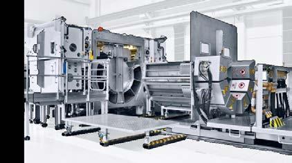
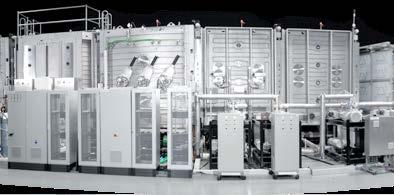
18 R2R Vacuum Processing Equipment Front surface contact free common platform Web support from back eliminates contact-based defects Winding versatility Low-friction roller bearings and optimized load cell positions for precise web tension Dual-bearing roller architecture to ensure roller-to-roller parallelism Supports a broad variety of substrate types and thicknesses Usable coating width 1.5 m R2R Vacuum Deposition Equipment Process Zones 18


19 PECVD: High Density Plasma Source Linear plasma source High-density plasma with low thermal budget High-quality film deposition Wide impedance range stability demonstrated CFD design to avoid powder buildup Laminar gas flow Uniform pressure distribution No dead or recirculation zones Plasma characteristics Plasma density > 1 x cm -3 Ion energy < 30 ev Electron temperature < 3 ev Plasma Uniformity Transmission / color ratio Full web width plasma uniformity ~± 2.5% Web Width (mm) 19
20 20


21 PVD: Rotary Cathode Technology Continuous target rotation ensures clean target surface Minimized particle buildup and emission Dramatically reduced ITO & IGZO nodule density &/or target crack density Maximized process stability and target utilization (> 80 %) Reduction of heat load to substrate during deposition with rotatable Lower target surface temperature with rotatable Less risk of film overheating Higher line speed on heat sensitive, thinner gauge substrates 21

22 Etch: Roll to Roll Etch Equipment R2R dry etch tools required for selective etching of silicon based semiconductor layers & dielectrics Utilizes fluorine & chlorine based chemistry for photoresist strip, silicon based dielectric & semiconductor etch & anisotropic metal etch Vision system required for inline microscopy & etch endpoint detection Commercial wet etchers available for source/gate/drain metal etching Requirement for selective process chemistry for etching different metals Multiple rinse step capability 200 o C anneal tunnel dryer HEPA filtered enclosure rated Class 100 or better 22

23 Imprint Lithography: Paradigm Shift in R2R Patterning Source : HP, 2009 Single mask, single imprint process with perfect source, gate & drain alignment!


24 Imprint Lithography Process Pixel speed depends linearly on mobility but inversely with the square of channel length ~40nm lines on 50μ polyimide 1μm Multilevel structures on flex at 5m/min 20 µm 4 levels in 0.5 μ step heights


25 TFT Backplane Imprint in Photoresist Provides basis for manufacture of TFT backplanes for active matrix driven sensors and low ppi displays in a-si and MO x (<200 ppi) Micron level features produced with excellent sidewall characteristics & aspect ratio Provides template for subsequent etch steps to manufacture device 1µm 25
26 Outline Introduction Megatrends Key R2R Process Technologies Barrier Films, Hardcoats & TFT Processing Summary 26
 &/or sensor manufacture Cover lens hardcoat")
27 Key R2R Technologies / Applications Substrate planarization Substrate barrier deposition Device passivation, encapsulation &/or barrier film deposition Low temperature TFT backplane manufacture Frontplane (EPD, EW & OLED) &/or sensor manufacture Cover lens hardcoat deposition

28 Multilayer Barrier Stacks Low temperature inorganic layer to inhibit H 2 O and O 2 permeation Defects in each inorganic layer impact permeation Low temperature process to avoid active organic layer degradation Multilayers critical to achieve high barrier for QD and OLED devices Redundancy and increase in effective diffusion path Planarization or burying of particles, defects by organic or quasi-organic layers Ref: Flexible Flat Panel Displays, Ed. G.P. Crawford (2005). Ref:- Robert Visser MIT/Stanford Nanoforum, April
29 Inorganic Layers for Barrier Films Material Deposition Method Conformal Coating AlOx PVD No line of sight deposition Cost Particle Size / Density High - low dep rate process SiOx PECVD Yes Low high dep rate process w/ HMDSO SiNx PECVD Yes Moderate high dep rate process w/sih 4 Microns/ high density Submicron/ high density Submicron/ low density Resistance to Acids Layer Density Fracture Toughness Low 3.2 g/cm MPa m 0.5 High 2.2 g/cm MPa m 0.5 High 2.7 g/cm MPa m 0.5 PECVD SiN x best choice for performance, cost, mechanical robustness Resistant to cracks during downstream processing and handling Key know-how from large area PECVD processes transferable to R2R High deposition rate and low cost processes for high quality films Particle mitigation strategies 29
30 Single Layer SiN x Barrier Performance Defect averaged barrier performance measured using Aquatran 2 permeation unit at 40 o C/100% RH conditions Barrier improvement factor increases linearly with SiN x layer thickness Typical WVTR ~ 1 x 10⁻³ g/m 2 day for SiN x layers on PET with MOCON (Ca test results >> 10 x lower) Typical WVTR at 20 o C/50% RH ~ 10 x lower than at 40 o C/100% RH 1 x 10⁻⁴ g/m 2 day Champion values as low as 7 x 10⁻⁴ g/m 2 day obtained on PET at 40 o C/100% RH 7 x 10⁻⁵ at 20 o C/50% RH 30

 Film RI DR nm m/min Uniformity % %T @400nm PP-HMDSO 1.")
31 Barrier Buffer Layer Development Quasi-organic interlayer required between SiN x layers to create torturous path Encapsulates particles and defects in place Mechanically decouples stiffer SiN x layers for increased stack flexibility High transmittance film when referenced to uncoated substrate Plasma Polymerized HMDSO (PP-HMDSO) Hexamethyldisiloxane (HMDSO) Film RI DR nm m/min Uniformity % PP-HMDSO 1.45 > 105 < 4% > 95% ~ 0 Stress MPa 31

32 Multilayer Stack Barrier Performance Defect averaged barrier performance measured using Aquatran 2 permeation unit at 40 o C/100% RH conditions WVTR < 7 x 10⁻⁵ g/m 2 day for full CVD 3 layer stack on PET Equivalent to < 7 x 10⁻⁶ g/m 2 day at 20 o C/50%RH 32
 through Adhesion Promotion")
33 Hardcoat for Next Generation Flexible Display Flexible hardcoat to replace current glass cover lens for bendable, rollable & foldable displays Abrasion resistant, UV stable & compatible with organics found in fingerprints R2R PECVD used to deposit tunable CTE siloxane based hardcoats on flexible substrates Pencil hardness improvement (4H 9H) through Adhesion Promotion Layers 33

34 R2R Process Flow: a-si:h Devices High grade, low surface roughness 50 µm PI foil used Bakeout required for mechanical stabilization & outgassing Plasma pretreated to enhance layer stack adhesion Deposition of barrier layer stack in CVD lab tool TFT layer stack deposition Al Gate metal layer deposited in PVD tool SiO 2 etch stop layer, SiN x gate dielectric, asi channel layer & n + contact layer deposited in CVD tool Cr source/drain metal layer deposited in PVD tool Device patterning Imprint lithography used to pattern stack in single step Coplanar device architecture Dry/wet etch steps used to provide final device structure 34
 expose")
35 SAIL Backplane: Patterning Process Flow Imprint Etch Disassemble Then Remove Next Etch Finally Etch top remove exposed polymer mask through metal the remove remaining polymer on array semiconductor and contact a stack top TFT gate second contact one metal stack polymer down all dielectric layer the time and layer to way at to a to to consisting define time expose to expose (optionally) expose the to TFT expose substrate gate completed channel area gate of the dielectric other covering lines structure. layers semiconductor undercutting layers that backplane covering TFT were Begin the by Top removing bottom channel isolated form the metal gate crossovers metal top by lines the metal undercut the thin regions Contact to isolate layer the (optional) gate lines and the Semiconductor TFTs Dielectric Bottom metal Process produces complete backplane: TFT Pixel electrode Data line Crossover Gate line


36 R2R TFT Device Performance Performance levels sufficient for sensor, EPD & electrowetting display applications High field effect mobility ~ 0.95 cm 2 /Vs for asi, ~ 10 cm 2 /Vs for IGZO High on/off current ratios ~ 10 8 for both asi and IGZO transistors Low threshold voltage ~ -2.5 V for asi & ~ 0.5 V for IGZO High threshold voltage drift stability < 0.4 V after 2000 s for asi 36
37 From Materials to Circuits Holistic toolbox approach required to build full circuits on flexible substrate materials for wearable device & IoT applications Hybrid solution required to optimize for cost & performance Number of steps & complexity of device will determine whether full R2R, R2S or S2S approach is required for yield and cost management Component performance & full scale device simulation required to reduce product development time and costs Materials Deposition Processes Etch Processes Lithography Bond/Interconnect Test/Repair Substrates Inorganic Layers Organic Layers Metals Inks Photoresists Adhesives PVD CVD Evaporation Printing Wet Etch Dry Etch Laser Ablation Photolithography Imprint Lithography Laser Ablation Flip Chip Printed Pads Low Temp Cure Pick & Place Optical Inspection Contact Probes Laser Trimming Laser CVD 37

38 Why Hybrid for Mobile, Wearable & IoT Devices? Essential for high performance applications Organics used in printed electronics not yet optimized for mobility & stability Atmospheric printing processes not yet accurate enough to compete with vacuum processed inorganic device stacks patterned with traditional lithography Substrate performance limits certain device types and integration paths Required for high resolution analog-digital conversion, RF communication, high density memory and certain logic applications Permits increased computational power, component density whilst reducing chip size with little compromise in total product form factor 38
39 Outline Introduction Megatrends Key R2R Process Technologies Barrier Films, Hardcoats & TFT Processing Summary 39
40 Roll-to-Roll Technology Roadmap Process Device Application Today Vacuum deposition Blanket films Touch sensors QDEF Barrier layers Optical coatings Food packaging Tomorrow Vacuum deposition Simple patterning Etch (dry & wet) Printing Blanket films Simple, passive optical & electronic devices Polarizers & plasmonic devices IoT devices Sensors Health, food spoilage & waste Future Vacuum deposition Complex patterning Etch (dry & wet) Printing Flex-hybrid integration Complex, active optical & electronic devices Low-resolution displays Flexible electronics Sensors Long-term roadmap to manufacture increasingly complex devices 40

41 Summary Displays & Flexible Electronics key drivers Information Universe R2R vacuum processing already in HVM for Touch Panel & Barriers Complex device architectures incl flexible TFT backplanes require R2R patterning Hybrid integration schemes required to combine the advantages of traditional silicon IC logic & memory with large scale integrated sensor & display devices Applied Materials creating building blocks to enable R2R manufacturing of more complex flexible devices and applications 41
42
Advances in Roll-to-Roll Imprint Lithography for Display Applications Using Self Aligned Imprint Lithography. John G Maltabes HP Labs
 Advances in Roll-to-Roll Imprint Lithography for Display Applications Using Self Aligned Imprint Lithography John G Maltabes HP Labs Outline Introduction Roll to Roll Challenges and Benefits HP Labs Roll
Advanced Display Manufacturing Technology
 Advanced Display Manufacturing Technology John Busch Vice President, New Business Development Display and Flexible Technology Group September 28, 2017 Safe Harbor This presentation contains forward-looking
Flexible Electronics Production Deployment on FPD Standards: Plastic Displays & Integrated Circuits. Stanislav Loboda R&D engineer
 Flexible Electronics Production Deployment on FPD Standards: Plastic Displays & Integrated Circuits Stanislav Loboda R&D engineer The world-first small-volume contract manufacturing for plastic TFT-arrays
AMOLED Manufacturing Process Report SAMPLE
 AMOLED Manufacturing Process Report SAMPLE 2018 AMOLED Manufacturing Process Report The report analyzes the structure and manufacturing process by dividing AMOLED into small & medium-sized rigid OLED,
Industrial Inline Control for Advanced Vacuum Roll to Roll Systems. Gerhard Steiniger Web inspection - surface Quallity control 7.
 Industrial Inline Control for Advanced Vacuum Roll to Roll Systems Gerhard Steiniger Web inspection - surface Quallity control 7.4-7684 1 Industrial Inline Control for Advanced Vacuum Roll to Roll Systems
Scalable self-aligned active matrix IGZO TFT backplane technology and its use in flexible semi-transparent image sensors. Albert van Breemen
 Scalable self-aligned active matrix IGZO TFT backplane technology and its use in flexible semi-transparent image sensors Albert van Breemen Image sensors today 1 Dominated by silicon based technology on
1. Publishable summary
 1. Publishable summary 1.1. Project objectives. The target of the project is to develop a highly reliable high brightness conformable low cost scalable display for demanding applications such as their
P I SCALE Creating an Open Access Flexible O L E D P ilo t L in e S e r vic e
 P I SCALE Creating an Open Access Flexible O L E D P ilo t L in e S e r vic e Pavel Kudlacek pavel.kudlacek@tno.nl P I - SCALE for 2017Flex 1 Lighting c h a lle n g e L ig h t in g c h a lle n g e At least
Enabling Paper-Like Displays Roll-to-Roll Manufacturing of Display Backplanes. Hewlett-Packard Company, Palo Alto, CA. Phicot Inc, Ames, IA
 Enabling Paper-Like Displays Roll-to-Roll Manufacturing of Display Backplanes Carl Taussig, Bob Cobene, Rich Elder, Warren Jackson, Mehrban Jam, Albert Jeans, Hao Luo, Ping Mei, Craig Perlov, Hewlett-Packard
Thin-Film Encapsulation of Organic Light Emitting Devices (OLEDs) Dr. Emilie Galand Huntsman Advanced Materials CSEM Plastic Optoelectronics - Basel
 Dr. Emilie Galand Huntsman Advanced Materials CSEM Plastic Optoelectronics - Basel") Thin-Film Encapsulation of Organic Light Emitting Devices (OLEDs) Dr. Emilie Galand CSEM Plastic Optoelectronics - Basel 25th June 2010 About Huntsman Huntsman is a global manufacturer and marketer of
Thin-Film Encapsulation of Organic Light Emitting Devices (OLEDs) Dr. Emilie Galand CSEM Plastic Optoelectronics - Basel 25th June 2010 About Huntsman Huntsman is a global manufacturer and marketer of
:: Reduce needs for heat dissipation components. :: Extend battery life in mobile products. :: Save power and reduce heat generation in TVs
 UniversalPHOLED Technology and Materials UniversalPHOLED Phosphorescent OLED technology and materials offer record-breaking performance to bring competitive advantages to your OLED display and lighting
FLEX2017 June, Monterey, USA Dr Mike Cowin, CMO, SmartKem.
 FLEX2017 June, Monterey, USA Dr Mike Cowin, CMO, SmartKem. FLEX2017 June, Monterey, USA Dr Mike Cowin, CMO, SmartKem. EU H2020 FLEXTRANs Grant Objectives A 24 month project (started September 2016) (Grant
ADDING AN O TO LEDS STATUS AND PERSPECTIVES OF ORGANIC LIGHT EMITTING DIODES PAWEL E. MALINOWSKI, TUNGHUEI KE LED EVENT 2017
 ADDING AN O TO LEDS STATUS AND PERSPECTIVES OF ORGANIC LIGHT EMITTING DIODES PAWEL E. MALINOWSKI, TUNGHUEI KE LIVING ROOM NOT SO LONG AGO... 2 Source: Warner Bros. Incadescent CRT 3 Source: Warner Bros.
New Worlds for Polymers: Organic Transistors, Light Emitting Diodes, and Optical Waveguides Ed Chandross
 New Worlds for Polymers: Organic Transistors, Light Emitting Diodes, and Optical Waveguides Ed Chandross Materials Chemistry, LLC 1 Polymers in the Electronic Industry Enabling Materials Active Materials?
Wafer Thinning and Thru-Silicon Vias
 Wafer Thinning and Thru-Silicon Vias The Path to Wafer Level Packaging jreche@trusi.com Summary A new dry etching technology Atmospheric Downstream Plasma (ADP) Etch Applications to Packaging Wafer Thinning
Display Technologies. Corning: The Technology Behind the Glass
 Display Technologies Corning: The Technology Behind the Glass Dr. David Chen Director, Application Engineering and Asia Commercial Technology Taiwan Corning Display Technologies Taiwan June 13, 2008 Forward
Next Generation of Poly-Si TFT Technology: Material Improvements and Novel Device Architectures for System-On-Panel (SOP)
") Next Generation of Poly-Si TFT Technology: Material Improvements and Novel Device Architectures for System-On-Panel (SOP) Tolis Voutsas* Paul Schuele* Bert Crowder* Pooran Joshi* Robert Sposili* Hidayat
Next Generation of Poly-Si TFT Technology: Material Improvements and Novel Device Architectures for System-On-Panel (SOP) Tolis Voutsas* Paul Schuele* Bert Crowder* Pooran Joshi* Robert Sposili* Hidayat
Phosphorescent OLED Technologies: The Next Wave. Plastic Electronics Conference Oct 9, 2012
 Phosphorescent OLED Technologies: The Next Wave Plastic Electronics Conference Oct 9, 2012 UDC Company Focus IP innovator, technology developer, patent licensor and materials supplier for the rapidly growing
Because Innovation Matters
 Because Innovation Matters Silicon Systems Group Toru Watanabe President, Applied Materials, Japan Semicon Japan November 30, 2010 Safe Harbor This presentation contains forward-looking statements, including
Applied Materials. 200mm Tools & Process Capabilities For Next Generation MEMS. Dr Michel (Mike) Rosa
 Rosa") Applied Materials 200mm Tools & Process Capabilities For Next Generation MEMS Dr Michel (Mike) Rosa 200mm MEMS Global Product / Marketing Manager, Components and Systems Group (CSG), Applied Global Services
Applied Materials 200mm Tools & Process Capabilities For Next Generation MEMS Dr Michel (Mike) Rosa 200mm MEMS Global Product / Marketing Manager, Components and Systems Group (CSG), Applied Global Services
The Company. A leading OLED player
 The Company A leading OLED player Novaled is the company to trade with, work for and invest in. Our company focuses on proprietary organic materials and complementary innovative technologies for superior
Overview of All Pixel Circuits for Active Matrix Organic Light Emitting Diode (AMOLED)
") Chapter 2 Overview of All Pixel Circuits for Active Matrix Organic Light Emitting Diode (AMOLED) ---------------------------------------------------------------------------------------------------------------
Chapter 2 Overview of All Pixel Circuits for Active Matrix Organic Light Emitting Diode (AMOLED) ---------------------------------------------------------------------------------------------------------------
Defect Analysis of Roll-to-Roll SAIL Manufactured Flexible Display Backplanes
 Defect Analysis of Roll-to-Roll SAIL Manufactured Flexible Display Backplanes Carl Taussig, Richard E. Elder, Warren B. Jackson, Albert Jeans, Mehrban Jam, Ed Holland, Hao Luo, John Maltabes, Craig Perlov,
projectors, head mounted displays in virtual or augmented reality use, electronic viewfinders
 Beatrice Beyer Figure 1. (OLED) microdisplay with a screen diagonal of 16 mm. Figure 2. CMOS cross section with OLED on top. Usually as small as fingernails, but of very high resolution Optical system
UV Nanoimprint Tool and Process Technology. S.V. Sreenivasan December 13 th, 2007
 UV Nanoimprint Tool and Process Technology S.V. Sreenivasan December 13 th, 2007 Agenda Introduction Need tool and process technology that can address: Patterning and CD control Alignment and Overlay Defect
Defense Technical Information Center Compilation Part Notice
 UNCLASSIFIED Defense Technical Information Center Compilation Part Notice ADPO1 1322 TITLE: Amorphous- Silicon Thin-Film Transistor With Two-Step Exposure Process DISTRIBUTION: Approved for public release,
Pressure sensor. Surface Micromachining. Residual stress gradients. Class of clean rooms. Clean Room. Surface micromachining
 Pressure sensor Surface Micromachining Deposit sacrificial layer Si PSG By HF Poly by XeF2 Pattern anchors Deposit/pattern structural layer Etch sacrificial layer Surface micromachining Structure sacrificial
ORGANIC ELECTRONICS PROCESS DEVELOPMENT AND ENCAPSULATION TECHNOLOGIES
 FRAUNHOFER INSTITUTE FOR ORGANIC ELECTRONICS, ELECTRON BEAM AND PLASMA TECHNOLOGY FEP ORGANIC ELECTRONICS PROCESS DEVELOPMENT AND ENCAPSULATION TECHNOLOGIES 2 PROFILE Fraunhofer FEP combines research and
OLED Status quo and our position
 OLED Status quo and our position Information Day 2013 A Deep Dive into the LC&OLED Business Dr. Udo Heider Vice President OLED Darmstadt, Germany June 26, 2013 Disclaimer Remarks All comparative figures
Leveraging 300 mm Technology Solutions to Enable New MEMS Process Capabilities
 Leveraging 300 mm Technology Solutions to Enable New MEMS Process Capabilities Evan Patton Semicon Europa November 2017 Lam Research Corp. 1 Presentation Outline The Internet of Things (IoT) as a market
 Chapter 1 Introduction --------------------------------------------------------------------------------------------------------------- 1.1 Overview of the Organic Light Emitting Diode (OLED) Displays Flat
Overcoming Challenges in 3D NAND Volume Manufacturing
 Overcoming Challenges in 3D NAND Volume Manufacturing Thorsten Lill Vice President, Etch Emerging Technologies and Systems Flash Memory Summit 2017, Santa Clara 2017 Lam Research Corp. Flash Memory Summit
Challenges for OLED Deposition by Vacuum Thermal Evaporation. D. W. Gotthold, M. O Steen, W. Luhman, S. Priddy, C. Counts, C.
 Challenges for OLED Deposition by Vacuum Thermal Evaporation D. W. Gotthold, M. O Steen, W. Luhman, S. Priddy, C. Counts, C. Roth June 7, 2011 Outline Introduction to Veeco Methods of OLED Deposition Cost
EQUIPMENT VACUUM WEB COATING SYSTEMS ROLL-TO-ROLL ROLL-TO-ROLL
 ROLL-TO-ROLL EQUIPMENT VACUUM WEB COATING SYSTEMS ROLL-TO-ROLL VACUUM WEB COATING APPLICATIONS VON ARDENNE provides tailored web coating solutions for today s most ambitious thin-film applications on polymer
Flexible Flat Panel Display Technology
 1 Flexible Flat Panel Display Technology Gregory P. Crawford Division of Engineering, Brown University, Providence RI 1.1 Introduction The manufacturing of flat panel displays is a dynamic and continuously
Present status of Roll-to-Roll Fabrication for OLED lighting
 Present status of Roll-to-Roll Fabrication for OLED lighting Michael Stanel, Tomasz Wański, Stefan Mogck Fraunhofer Institute for Organic Electronics, Electron Beam and Plasma Technology FEP AIMCAL, Web
AIXTRON in EXCILIGHT project
 AIXTRON SE AIXTRON in EXCILIGHT project Gintautas Simkus ABOUT AIXTRON 2 Who we are Headquarter based in Herzogenrath, Germany Worldwide presence with 14 sales/representatives offices and production facilities
TipatOr. Liquid metal switch (LMS) display technology. Avi Fogel
 display technology. Avi Fogel") TipatOr Liquid metal switch (LMS) display technology Avi Fogel 972-52-5702938 avifog@gmail.com Who is behind TipatOr TipatOr emerged from a merger of 2 expert groups in the fields of MEMS and Displays
TipatOr Liquid metal switch (LMS) display technology Avi Fogel 972-52-5702938 avifog@gmail.com Who is behind TipatOr TipatOr emerged from a merger of 2 expert groups in the fields of MEMS and Displays
Principles of Electrostatic Chucks 6 Rf Chuck Edge Design
 Principles of Electrostatic Chucks 6 Rf Chuck Edge Design Overview This document addresses the following chuck edge design issues: Device yield through system uniformity and particle reduction; System
Semiconductors Displays Semiconductor Manufacturing and Inspection Equipment Scientific Instruments
 Semiconductors Displays Semiconductor Manufacturing and Inspection Equipment Scientific Instruments Electronics 110-nm CMOS ASIC HDL4P Series with High-speed I/O Interfaces Hitachi has released the high-performance
Deep Silicon Etch Technology for Advanced MEMS Applications
 Deep Silicon Etch Technology for Advanced MEMS Applications Shenjian Liu, Ph.D. Managing Director, AMEC AMEC Company Profile and Product Line-up AMEC HQ, R&D and MF Facility in Shanghai AMEC Taiwan AMEC
Technology Overview LTCC
 Sheet Code RFi0604 Technology Overview LTCC Low Temperature Co-fired Ceramic (LTCC) is a multilayer ceramic substrate technology that allows the realisation of multiple embedded passive components (Rs,
Content. Core Technology (Short introduction) LCMO (Light Controlled Molecular Orientation) technology
 LCMO (Light Controlled Molecular Orientation) technology") Content Core Technology (Short introduction) LCMO (Light Controlled Molecular Orientation) technology LCMO Patterned Films for Light management : Applications Examples LCMO- Photo Patterned Retarders LCMO-
Content Core Technology (Short introduction) LCMO (Light Controlled Molecular Orientation) technology LCMO Patterned Films for Light management : Applications Examples LCMO- Photo Patterned Retarders LCMO-
Organic light emitting diode (OLED) displays
 displays") Ultra-Short Pulse Lasers Enable Precision Flexible OLED Cutting FLORENT THIBAULT, PRODUCT LINE MANAGER, HATIM HALOUI, APPLICATION MANAGER, JORIS VAN NUNEN, PRODUCT MARKETING MANAGER, INDUSTRIAL PICOSECOND
Ultra-Short Pulse Lasers Enable Precision Flexible OLED Cutting FLORENT THIBAULT, PRODUCT LINE MANAGER, HATIM HALOUI, APPLICATION MANAGER, JORIS VAN NUNEN, PRODUCT MARKETING MANAGER, INDUSTRIAL PICOSECOND
Liquid Crystal Display (LCD)
") Liquid Crystal Display (LCD) When coming into contact with grooved surface in a fixed direction, liquid crystal molecules line up parallelly along the grooves. When coming into contact with grooved surface
Liquid Crystal Display (LCD) When coming into contact with grooved surface in a fixed direction, liquid crystal molecules line up parallelly along the grooves. When coming into contact with grooved surface
Comparative Analysis of Organic Thin Film Transistor Structures for Flexible E-Paper and AMOLED Displays
 Comparative Analysis of Organic Thin Film Transistor Structures for Flexible E-Paper and AMOLED Displays Linrun Feng, Xiaoli Xu and Xiaojun Guo ECS Trans. 2011, Volume 37, Issue 1, Pages 105-112. doi:
Forward-Looking Statements
 Forward-Looking Statements Information in this presentation regarding MagnaChip s forecasts, business outlook, expectations and beliefs are forward-looking statements within the meaning of the Private
Self-Aligned Double Patterning for 3xnm Flash Production
 Self-Aligned Double Patterning for 3xnm Flash Production Chris Ngai Dir of Process Engineering & Lithography Maydan Technology Center Group Applied Materials, Inc. July 16 th, 2008 Overview Double Patterning
[1.9] AMOLED 공정 Introduction OLED Materials Patterning Process Process Equipments
![[1.9] AMOLED 공정 Introduction OLED Materials Patterning Process Process Equipments](/thumbs/73/69073032.jpg "[1.9] AMOLED 공정 Introduction OLED Materials Patterning Process Process Equipments") [1.9] AMOLED 공정 1.9.1. Introduction 1.9.2. OLED Materials 1.9.3. Patterning Process 1.9.4. Process Equipments OLED : Organic Light Emitting Diode Organic EL : Organic Electroluminescent 재료및공정 재료의발광메카니즘
[1.9] AMOLED 공정 1.9.1. Introduction 1.9.2. OLED Materials 1.9.3. Patterning Process 1.9.4. Process Equipments OLED : Organic Light Emitting Diode Organic EL : Organic Electroluminescent 재료및공정 재료의발광메카니즘
VACUUM WEB COATING SYSTEMS ROLL-TO-ROLL ROLL-TO-ROLL VACUUM WEB COATING SYSTEMS
 VACUUM WEB COATING SYSTEMS ROLL-TO-ROLL ROLL-TO-ROLL VACUUM WEB COATING SYSTEMS VACUUM WEB COATING APPLICATIONS VON ARDENNE provides tailored web coating solutions for today s most ambitious thin-film
Development of OLED Lighting Applications Using Phosphorescent Emission System
 Development of OLED Lighting Applications Using Phosphorescent Emission System Kazuhiro Oikawa R&D Department OLED Lighting Business Center KONICA MINOLTA ADVANCED LAYERS, INC. October 10, 2012 Outline
Leading. Through Innovation. Film Technology Franchise. September 9, 2008
 Film Technology Franchise Steven Webster, VP, Research & Technology Commercialization Display & Graphics Business Leading Through Innovation September 9, 2008 1 3M s Film Franchise Is More Than Optical
HB LEDs & OLEDs. Complete thin film process solutions
 HB LEDs & OLEDs Complete thin film process solutions Get off to a flying start for all your LED thin film deposition and etch processes From 2 inch to 8 inch Manual or fully automated substrate handling
Joint Development of Ultra-Bright, Inorganic EL Light-Emitting Materials. November 2, 2005 KURARAY CO., LTD.
 Joint Development of Ultra-Bright, Inorganic EL Light-Emitting Materials November 2, 2005 KURARAY CO., LTD. Sales Trends of Display-related Products (Kuraray (standalone)) FY1994 FY1999 FY2004 Sales Ratio
PROCESS TECHNOLOGIES FOR ADVANCED ORGANIC ELECTRONIC DEVICES: MICRODISPLAYS, LIGHTING AND SOLAR CELLS
 PROCESS TECHNOLOGIES FOR ADVANCED ORGANIC ELECTRONIC DEVICES: MICRODISPLAYS, LIGHTING AND SOLAR CELLS Dr. Christian May Fraunhofer IPMS - Center for Organic Materials and Electronic Devices Dresden COMEDD
SPATIAL LIGHT MODULATORS
 SPATIAL LIGHT MODULATORS Reflective XY Series Phase and Amplitude 512x512 A spatial light modulator (SLM) is an electrically programmable device that modulates light according to a fixed spatial (pixel)
P-224: Damage-Free Cathode Coating Process for OLEDs
 P-224: Damage-Free Cathode Coating Process for OLEDs Shiva Prakash DuPont Displays, 6 Ward Drive, Santa Barbara, CA 937, USA Abstract OLED displays require the growth of inorganic films over organic films.
MicroLED Displays: Global Trends & Opportunities for Equipment and Material Suppliers
 Picture: Sony From Technologies to Market MicroLED Displays: Global Trends & Opportunities for Equipment and Material Suppliers SEMICON EUROPA Jean-Christophe ELOY - CEO - Yole Développement 2017 AGENDA
Design of Organic TFT Pixel Electrode Circuit for Active-Matrix OLED Displays
 JOURNAL OF COMPUTERS, VOL. 3, NO. 3, MARCH 2008 1 Design of Organic TFT Pixel Electrode Circuit for Active-Matrix Displays Aram Shin, Sang Jun Hwang, Seung Woo Yu, and Man Young Sung 1) Semiconductor and
The Transition to Patterned Media in Hard Disk Drives
 The Transition to Patterned Media in Hard Disk Drives The Evolution of Jet and Flash Imprint Lithography for Patterned Media DISKCON San Jose Sept 24 rd, 2009 Paul Hofemann, Vice President, HDD Future
Technology White Paper Plasma Displays. NEC Technologies Visual Systems Division
 Technology White Paper Plasma Displays NEC Technologies Visual Systems Division May 1998 1 What is a Color Plasma Display Panel? The term Plasma refers to a flat panel display technology that utilizes
FIRST CALL FOR PAPERS SID Society for Information Display INTERNATIONAL SYMPOSIUM, SEMINAR & EXHIBITION. May 19 24, 2013
 FIRST CALL FOR PAPERS SID 2013 Society for Information Display INTERNATIONAL SYMPOSIUM, SEMINAR & EXHIBITION May 19 24, 2013 VANCOUVER CONVENTION CENTER VANCOUVER, BRITISH COLUMBIA, CANADA SID SOCIETY
Transforming Electronic Interconnect Breaking through historical boundaries Tim Olson Founder & CTO
 Transforming Electronic Interconnect Breaking through historical boundaries Tim Olson Founder & CTO Remember when? There were three distinct industries Wafer Foundries SATS EMS Semiconductor Devices Nanometers
 Chapter 3 Evaluated Results of Conventional Pixel Circuit, Other Compensation Circuits and Proposed Pixel Circuits for Active Matrix Organic Light Emitting Diodes (AMOLEDs) -------------------------------------------------------------------------------------------------------
Reduction of Device Damage During Dry Etching of Advanced MMIC Devices Using Optical Emission Spectroscopy
 Reduction of Device Damage During Dry Etching of Advanced MMIC Devices Using Optical Emission Spectroscopy D. Johnson, R. Westerman, M. DeVre, Y. Lee, J. Sasserath Unaxis USA, Inc. 10050 16 th Street North
High Repetition Rate USP Lasers Improve OLED Cutting Results
 Coherent White Paper May 7, 2018 High Repetition Rate USP Lasers Improve OLED Cutting Results High power ultraviolet, picosecond industrial lasers are widely employed because of their proven ability to
Organic light emitting diodes for display technology
 Organic light emitting diodes for display technology Shamna Shamsudeen MScTI - ZITI-Heidelberg University OLED ZITI, Uni Heidelberg Page1 What s Light Light: Visible part of EM spectra. Ref:[1] Thermoluminescence:
FASwitch - A MEMS Display Backplane Manufactured by Flex Circuit Methods
 FASwitch - A MEMS Display Backplane Manufactured by Flex Circuit Methods Presenter: Dr. Nicholas F. Pasch Rolltronics Corporation 750 Menlo Ave. Menlo Park, CA 94025 npasch@rolltronics.com Introduction
EQUIPMENT COATING SYSTEMS FOR THIN-FILM PV THIN-FILM PHOTOVOLTAICS. SCALA VISS PIA nova GC120VCR XENIA
 THIN-FILM PHOTOVOLTAICS EQUIPMENT COATING SYSTEMS FOR THIN-FILM PV SCALA VISS PIA nova GC120VCR XENIA OUR STORY. OUR EXPERIENCE. RANGE OF APPLICATIONS VON ARDENNE provides advanced PVD coating equipment
SINGULATION BY PLASMA ETCHING. INTEGRATION TECHNIQUES TO ENABLE LOW DAMAGE, HIGH PRODUCTIVITY DICING.
 SINGULATION BY PLASMA ETCHING. INTEGRATION TECHNIQUES TO ENABLE LOW DAMAGE, HIGH PRODUCTIVITY DICING. Richard Barnett Dave Thomas Oliver Ansell ABSTRACT Plasma dicing has rapidly gained traction as a viable
CCD Element Linear Image Sensor CCD Element Line Scan Image Sensor
 1024-Element Linear Image Sensor CCD 134 1024-Element Line Scan Image Sensor FEATURES 1024 x 1 photosite array 13µm x 13µm photosites on 13µm pitch Anti-blooming and integration control Enhanced spectral
SUPPLEMENTARY INFORMATION
 User-interactive electronic-skin for instantaneous pressure visualization Chuan Wang 1,2,3, David Hwang 1,2,3, Zhibin Yu 1,2,3, Kuniharu Takei 1,2,3, Junwoo Park 4, Teresa Chen 4, Biwu Ma 3,4, and Ali
Nano-Imprint Lithography Infrastructure: Imprint Templates
 Nano-Imprint Lithography Infrastructure: Imprint Templates John Maltabes Photronics, Inc Austin, TX 1 Questions to keep in mind Imprint template manufacturability Resolution Can you get sub30nm images?
Abstract. Keywords INTRODUCTION. Electron beam has been increasingly used for defect inspection in IC chip
 Abstract Based on failure analysis data the estimated failure mechanism in capacitor like device structures was simulated on wafer in Front End of Line. In the study the optimal process step for electron
Etching Part 2. Saroj Kumar Patra. TFE4180 Semiconductor Manufacturing Technology. Norwegian University of Science and Technology ( NTNU )
") 1 Etching Part 2 Chapter : 16 Semiconductor Manufacturing Technology by M. Quirk & J. Serda Spring Semester 2014 Saroj Kumar Patra, Norwegian University of Science and Technology ( NTNU ) 2 Introduction
1 Etching Part 2 Chapter : 16 Semiconductor Manufacturing Technology by M. Quirk & J. Serda Spring Semester 2014 Saroj Kumar Patra, Norwegian University of Science and Technology ( NTNU ) 2 Introduction
The future of microled displays using nextgeneration
 The future of microled displays using nextgeneration technologies Introduction MicroLEDs (micro-light-emitting diodes) are an emerging display technology that, as the name implies, use very small LEDs
THE NEXT LEVEL IN ARCHITECTURAL GLASS COATING ADVANCED EQUIPMENT & PROCESS EXPERTISE ADVANCED EQUIPMENT & PROCESS EXPERTISE
 THE NEXT LEVEL IN ARCHITECTURAL GLASS COATING ADVANCED EQUIPMENT & PROCESS EXPERTISE THE NEXT LEVEL IN ARCHITECTURAL GLASS COATING ADVANCED EQUIPMENT & PROCESS EXPERTISE ARCHITECTURAL GLASS COATING REACHES
Development of OLED Lighting Panel with World-class Practical Performance
 72 Development of OLED Lighting Panel with World-class Practical Performance TAKAMURA MAKOTO *1 TANAKA JUNICHI *2 MORIMOTO MITSURU *2 MORI KOICHI *3 HORI KEIICHI *4 MUSHA MASANORI *5 Using its proprietary
High ResolutionCross Strip Anodes for Photon Counting detectors
 High ResolutionCross Strip Anodes for Photon Counting detectors Oswald H.W. Siegmund, Anton S. Tremsin, Robert Abiad, J. Hull and John V. Vallerga Space Sciences Laboratory University of California Berkeley,
Solution-based transistor matrix
 18 PRINTED ELECTRONICS Solution-based transistor matrix A groundbreaking new technology is making it far more cost-effective to produce the electronic control unit of liquid crystal displays. At the same
CCD 143A 2048-Element High Speed Linear Image Sensor
 A CCD 143A 2048-Element High Speed Linear Image Sensor FEATURES 2048 x 1 photosite array 13µm x 13µm photosites on 13µm pitch High speed = up to 20MHz data rates Enhanced spectral response Low dark signal
Automation in Semiconductor Manufacturing IEDM, San Francisco, 1982 Keynote Speech
 Automation in Semiconductor Manufacturing IEDM, San Francisco, 1982 Keynote Speech Commentary Alongside ISSCC, IEDM is the most traditional academic conference in the semiconductor field, and it is held
Digital Light Processing
 A Seminar report On Digital Light Processing Submitted in partial fulfillment of the requirement for the award of degree of Bachelor of Technology in Computer Science SUBMITTED TO: www.studymafia.org SUBMITTED
LG OLED Light Panel. Flexible panels
 LG OLED Light Panel Flexible panels Handling Instruction A. Handling and Safety 1. Unpack packing box with care. Remove packing trays gently and carefully from packing box. 2. During unloading and handling,
Sep 09, APPLICATION NOTE 1193 Electronic Displays Comparison
 Sep 09, 2002 APPLICATION NOTE 1193 Electronic s Comparison Abstract: This note compares advantages and disadvantages of Cathode Ray Tubes, Electro-Luminescent, Flip- Dot, Incandescent Light Bulbs, Liquid
These are used for producing a narrow and sharply focus beam of electrons.
 CATHOD RAY TUBE (CRT) A CRT is an electronic tube designed to display electrical data. The basic CRT consists of four major components. 1. Electron Gun 2. Focussing & Accelerating Anodes 3. Horizontal
OLED ON CMOS: WHAT ABOUT THINNING AND BENDING?
 Large cost-effective OLED microdisplays and their applications OLED ON CMOS: WHAT ABOUT THINNING AND BENDING? IDW2017 tony.maindron@cea.fr T. Maindron, B. Chambion, A. Vandeneynde, S. Gétin, M. Provost,
MAXIM INTEGRATED PRODUCTS
 RELIABILITY REPORT FOR PLASTIC ENCAPSULATED DEVICES May 4, 2009 MAXIM INTEGRATED PRODUCTS 120 SAN GABRIEL DR. SUNNYVALE, CA 94086 Approved by Ken Wendel Quality Assurance Director, Reliability Engineering
Application note. Materials. Introduction. Authors. Travis Burt, Huang ChuanXu*, Andy Jiang* Agilent Technologies Mulgrave, Victoria, Australia
 Performance of compact visual displays measuring angular reflectance of optically active materials using the Agilent Cary 7000 Universal Measurement Spectrophotometer (UMS) Application note Materials Authors
Rollable Display Coming to Reality Interviews with World s First 18-inch Flexible Display Developers
 Rollable Display Coming to Reality Interviews with World s First 18-inch Flexible Display Developers Transparent displays and rollable displays are coming into our daily lives, just like science fiction
PUBLISHABLE Summary To provide OLED stacks with improved reliability Provide improved thin film encapsulation
 PUBLISHABLE Summary SCOOP is a European funded project (FP7 project number 287595 SCOOP). It is focused on OLED technology, microdisplays based on the combination of OLED with CMOS technology, and innovative
Spatial Light Modulators XY Series
 Spatial Light Modulators XY Series Phase and Amplitude 512x512 and 256x256 A spatial light modulator (SLM) is an electrically programmable device that modulates light according to a fixed spatial (pixel)
Monolithic Optoelectronic Integration of High- Voltage Power FETs and LEDs
 Monolithic Optoelectronic Integration of High- Voltage Power FETs and LEDs, Zhongda Li, Robert Karlicek and T. Paul Chow Smart Lighting Engineering Research Center Rensselaer Polytechnic Institute, Troy,
Fabrication of Lithium Niobate nanopillars using Focused Ion Beam (FIB)
") Fabrication of Lithium Niobate nanopillars using Focused Ion Beam (FIB) Final report for Nanofabrication with Focused Ion and Electron beams course (SK3750) Amin Baghban June 2015 1- Introduction Thanks
Fabrication of Lithium Niobate nanopillars using Focused Ion Beam (FIB) Final report for Nanofabrication with Focused Ion and Electron beams course (SK3750) Amin Baghban June 2015 1- Introduction Thanks
New Rotary Magnetron Magnet Bar Improves Target Utilization and Deposition Uniformity
 Society of Vacuum Coaters 2013 Technical Conference Presentation New Rotary Magnetron Magnet Bar Improves Target Utilization and Deposition Uniformity John Madocks & Phong Ngo, General Plasma Inc., 546
SNU PRECISION CO., LTD
 SNU PRECISION CO., LTD 1629-2 Nakseongdae-dong, Kwanak-ku in Seoul, SOUTH KOREA The First Quarter 2011 Disclaimer This document has been prepared by SNU Precision CO., Ltd.( the Company ). Until 2010,
OLED Lighting in Automotive Applications State of the Art and Future Demands. OLEDs World Summit 2017, San Francisco, Dr. Werner Thomas, AUDI AG
 OLED Lighting in Automotive Applications State of the Art and Future Demands OLEDs World Summit 2017, San Francisco, Dr. Werner Thomas, AUDI AG 2 Agenda 1. Overview 1 st automotive series applications
The Flat Panel Display Paradigm: Successful Implementation of Microelectronic Processes on Gigantic Wafers
 The Flat Panel Display Paradigm: Successful Implementation of Microelectronic Processes on Gigantic Wafers Dr. Zvi Yaniv Applied Nanotech, Inc. 3006 Longhorn Blvd., Suite 107 Austin, TX 78758 Phone 512-339-5020
Solid State Devices 4B6
 Solid State Devices 4B6 Lecture 13 Projection and 3D displays: LCD, DLP and LCOS Daping Chu Lent 2016 Development of flat panel displays (FPDs) (LCD) in early days 1 A 105 inch TFT-LCD 4k2k curved panel