Because Innovation Matters
|
|
|
- Chad Walters
- 5 years ago
- Views:
Transcription
1 Because Innovation Matters Silicon Systems Group Toru Watanabe President, Applied Materials, Japan Semicon Japan November 30, 2010
2 Safe Harbor This presentation contains forward-looking statements, including those regarding the Applied Silicon Systems Group s performance, strategic positions, products and opportunities. These statements are subject to known and unknown risks and uncertainties that could cause actual results to differ materially from those expressed or implied by such statements, including but not limited to: the level of demand for Applied s products, which is subject to many factors, including: uncertain global economic and industry conditions, business and consumer spending, demand for electronic products and semiconductors, and customers utilization rates and new technology and capacity requirements; Applied s ability to (i) develop, deliver and support a broad range of products, expand its markets and develop new markets, (ii) align its cost structure with business conditions, (iii) plan and manage its resources and production capability, (iv) implement initiatives that enhance global operations and efficiencies, (v) maintain effective internal controls and procedures, (vi) obtain and protect intellectual property rights in key technologies, and (vii) attract, motivate and retain key employees; risks related to legal proceedings and claims; and other risks described in Applied s SEC filings. All forward-looking statements are based on management s estimates, projections and assumptions as of November 30, 2010, and Applied undertakes no obligation to update any forward-looking statements..
3 Silicon Systems Group Overview #1 in the WFE and advanced packaging markets In 2010, expect increased market share in each SSG business In 2011, expect to grow WFE market share for the 3 rd consecutive year Growth fueled by new product innovations aligned to technology inflections Source: Gartner, April
4 Innovations Enable Inflections ADVANCED PATTERNING WAFER-LEVEL PACKAGING TRANSISTOR INTERCONNECT Centris Etch Tetra X Silvia Etch Eterna FCVD Aera3 Avila CVD Avenir PVD/ALD Mesa Etch InVia CVD Siconi for Epi Centinel PVD UVision 4 Brightfield Raider-S ECD Astra DSA Anneal Reflexion GT CMP Accelerating innovations 15 new products in 15 months 4
5 Applied Materials Conductor Etch Innovations Ellie Yieh VP and GM, Etch Business Unit Semicon Japan November 30, 2010
6 Conductor Etch is Fastest Growing Etch Segment Conductor etch ~ $1.6B market in 2010 New steps in advanced transistors, double patterning and advanced packaging driving growth Applied already leads in advanced DRAM transistor critical etch Source: Gartner, Sept
7 Innovations Enable Inflections ADVANCED PATTERNING WAFER-LEVEL PACKAGING TRANSISTOR INTERCONNECT Centris Etch Tetra X Silvia Etch Eterna FCVD Aera3 Avila CVD Avenir PVD/ALD Mesa Etch InVia CVD Siconi for Epi Centinel PVD UVision 4 Brightfield Raider-S ECD Astra DSA Anneal Reflexion GT CMP Accelerating innovations 15 new products in 15 months 7


8 Applied s Conductor Etch Competitive Position VERTICAL SCALING Leading in Advanced DRAM (BBL/BWL architectures) HORIZONTAL SCALING Expanding Positions in Double Patterning NAND, Foundry, Logic and DRAM Requires <1 % Depth Non-Uniformity Requires <1 nm, 3σ CD Non-Uniformity 8
9 Gap in Litho Roadmap is Etch Opportunity 10 Above Wavelength Near Wavelength Below Wavelength Double Patterning Resolution (µm) g-line λ=436nm i-line λ=365nm DUV λ=248nm Hard Mask Insertion 193 (dry) λ=193nm (immersion) λ=193nm F Year of Production Lithography Gap Hard masks and double patterning enable below-wavelength patterning Sources: 2010 ITRS Roadmap, Applied Materials 9
10 Adding up the CD Variation Logic / Foundry Double Patterning Scheme L 1 = First litho CD variation E 2 = First hard mask etch CD variation L 3 + L 4 = Second litho CD + overlay variation E 5 = Second hard mask etch CD variation Yield impacted by CD variation: (L 1, E 2, L 3, L 4, E 5 ) Tighter etch CD uniformity can give wider process window for litho 10

11 How Precise is the Etched Critical Dimension? Red Blood Cells Etched CD variation range of 0.8 nm: 10,000X smaller than a red blood cell diameter, matched over thousands of wafers 11

12 Patterning Etch Steps Growing +6 steps NAND 4X nm NAND 2X nm +10 steps Logic 45 nm Logic 22 nm +10 steps DRAM 4X nm DRAM 2X nm Source: Applied Materials estimate Added steps increase process cost for customers 12

13 Relentless Cost-per-Bit Reduction $ / MB F F Source: Gartner, Applied Materials Cost reduction is key for customers 13


14 Applied s Etch Leadership in Productivity and Technology Improved CD Control Traditional Platform Centris Platform Lower Cost-Per-Wafer (normalized) 30% lower cost-per-wafer with leading critical etch performance 14
15 Applied s Centris Platform: Performance Worth Repeating Combines industry-leading Mesa chambers with high-productivity Centris platform 15


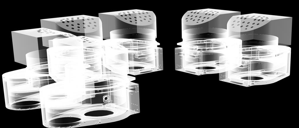
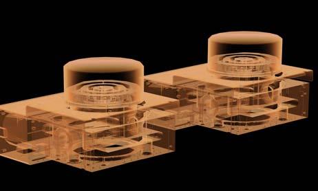
16 Building a Productivity Powerhouse with Centris 6 Mesa Chambers Dual- Blade Robot En-Route Abatement Four- FOUP Interface Optimized Gas Panel


17 Seijo En-Route Abatement Doubles the Number of Etch Chambers 3 Etch Chambers Traditional Platform Centris Platform 6 Etch Chambers Abatement Chamber 4 process chambers total 2 Seijo Abatement Chambers 8 process chambers total


18 AdvantEdge Mesa Chamber: Angstrom-level Precise Etch Mesa Source <1nm CD Uniformity <1% Etch Depth Uniformity Pulsync Extending Silicon Etch Memory leadership 1 st ultra-flat uniformity ICP* etcher enabling 3xnm node Rapid adoption with >200 chambers in 9 months Source Bias Pulse Pulse * Inductively Coupled Plasma Advanced plasma control Microloading benefit 18


19 Mesa Source: Breakthrough Etch Rate Uniformity Traditional Mesa Limited Electrical Field Tunability Electrical Field Decoupled and Tunable Limited Uniformity Improved Uniformity Breakthrough Mesa source delivers ultra-flat etch rate map 19
20 Mesa Pulsync Mitigates Microloading Challenge: Bi-Modal Trench Depth Distribution with Spacer Double Patterning SEVERE LOADING No Pulsing MINIMAL LOADING With Pulsync Mesa s Pulsync technology minimizes micro-loading in etch depth SEM image used with customer permission 20


21 Centris Enables the Same CD Every Time 6 Mesa Chambers, Auto- Calibrated to Same Standard Central Reference Standards Auto- Calibration Management Software E3 software identifies excursions
22 Improved Process Parameter Repeatability via Auto-Calibration OLD CONTROL LIMIT Base Pressure NEW CONTROL LIMIT Ch A Ch B Ch C Ch D Ch E Ch F Autocalibration off Autocalibration on Time (days) 22 Patent Applied For
23 Centris Etch Matching of 4,000 Wafers 43.0 Post-Process CD (nm) Upper Spec Limit Lower Spec Limit Number of wafers Chamber matching demonstrated at 0.8nm range across 4,000 wafers 23
24 Device Yield Benefit from Tighter Controls Traditional Platform Centris Platform PRODUCT PERFORMANCE PROCESS PERFORMANCE Device Yield Device Yield 24
25 Capital Productivity Benefit for Customers NAND 2Xnm at 250K WSPM, One Etch Application 3 ETCH, 1 ABATEMENT PLATFORM 6 ETCH, 2 EN-ROUTE ABATEMENT PLATFORM Unique 8-chamber architecture enables best-in-class productivity


26 Green Benefits of Lower Facilitization Costs ~35% improvement in energy savings from standard etchers One Platform saves an Olympicsize swimming pool of water per year Lower CO 2 emissions per Platform: equivalent to taking 50 cars per year off the road Green benefits contribute one-third of cost-per-wafer savings Assumes SEMI S23 standard calculations 26
27 Applied s Conductor Etch Platforms are Well Positioned at Leading Customers AdvantEdge Chamber AdvantEdge Mesa Chamber Centris Platform >1500 chambers >200 chambers in first 9 months 5 customers; includes entry into 2 new customers 27

28 Applied s Centris Platform: Performance Worth Repeating Precise Intelligent Productive Tightest CD uniformity Tightest depth uniformity on each wafer Auto-calibrating Industry-leading at 30% lower cost-per-wafer 28

29
Self-Aligned Double Patterning for 3xnm Flash Production
 Self-Aligned Double Patterning for 3xnm Flash Production Chris Ngai Dir of Process Engineering & Lithography Maydan Technology Center Group Applied Materials, Inc. July 16 th, 2008 Overview Double Patterning
Advanced Display Manufacturing Technology
 Advanced Display Manufacturing Technology John Busch Vice President, New Business Development Display and Flexible Technology Group September 28, 2017 Safe Harbor This presentation contains forward-looking
Applied Materials. 200mm Tools & Process Capabilities For Next Generation MEMS. Dr Michel (Mike) Rosa
 Rosa") Applied Materials 200mm Tools & Process Capabilities For Next Generation MEMS Dr Michel (Mike) Rosa 200mm MEMS Global Product / Marketing Manager, Components and Systems Group (CSG), Applied Global Services
Applied Materials 200mm Tools & Process Capabilities For Next Generation MEMS Dr Michel (Mike) Rosa 200mm MEMS Global Product / Marketing Manager, Components and Systems Group (CSG), Applied Global Services
Reduction of Device Damage During Dry Etching of Advanced MMIC Devices Using Optical Emission Spectroscopy
 Reduction of Device Damage During Dry Etching of Advanced MMIC Devices Using Optical Emission Spectroscopy D. Johnson, R. Westerman, M. DeVre, Y. Lee, J. Sasserath Unaxis USA, Inc. 10050 16 th Street North
Approaching Zero Etch Bias at Cr Etch Process
 Approaching Zero Etch Bias at Cr Etch Process Pavel Nesladek a ; Norbert Falk b ; Andreas Wiswesser a ; Renee Koch b ; Björn Sass a a Advanced Mask Technology Center, Rähnitzer Allee 9; 01109 Dresden,
Readiness and Challenges of EUV Mask
 Panel Discussion: EUVL HVM Insertion and Scaling Readiness and Challenges of EUV Mask Takashi Kamo Toshiba Corporation Semiconductor & Storage Products Company Contents [1] Introduction [2] EUV Mask Defect
Leveraging 300 mm Technology Solutions to Enable New MEMS Process Capabilities
 Leveraging 300 mm Technology Solutions to Enable New MEMS Process Capabilities Evan Patton Semicon Europa November 2017 Lam Research Corp. 1 Presentation Outline The Internet of Things (IoT) as a market
DOUBLE PATTERNING CHALLENGES FOR 20nm TECHNOLOGY
 DOUBLE PATTERNING CHALLENGES FOR 20nm TECHNOLOGY SEMICON DRESDEN TechARENA OCTOBER 12 th 2011 Vincent Farys, Bertrand Le-Gratiet, Pierre-Jérôme Goirand STMicroelectronics Crolles 2 OUTLINE Lithography
Wafer Thinning and Thru-Silicon Vias
 Wafer Thinning and Thru-Silicon Vias The Path to Wafer Level Packaging jreche@trusi.com Summary A new dry etching technology Atmospheric Downstream Plasma (ADP) Etch Applications to Packaging Wafer Thinning
The Transition to Patterned Media in Hard Disk Drives
 The Transition to Patterned Media in Hard Disk Drives The Evolution of Jet and Flash Imprint Lithography for Patterned Media DISKCON San Jose Sept 24 rd, 2009 Paul Hofemann, Vice President, HDD Future
Deep Silicon Etch Technology for Advanced MEMS Applications
 Deep Silicon Etch Technology for Advanced MEMS Applications Shenjian Liu, Ph.D. Managing Director, AMEC AMEC Company Profile and Product Line-up AMEC HQ, R&D and MF Facility in Shanghai AMEC Taiwan AMEC
Monolithic Optoelectronic Integration of High- Voltage Power FETs and LEDs
 Monolithic Optoelectronic Integration of High- Voltage Power FETs and LEDs, Zhongda Li, Robert Karlicek and T. Paul Chow Smart Lighting Engineering Research Center Rensselaer Polytechnic Institute, Troy,
Etching Part 2. Saroj Kumar Patra. TFE4180 Semiconductor Manufacturing Technology. Norwegian University of Science and Technology ( NTNU )
") 1 Etching Part 2 Chapter : 16 Semiconductor Manufacturing Technology by M. Quirk & J. Serda Spring Semester 2014 Saroj Kumar Patra, Norwegian University of Science and Technology ( NTNU ) 2 Introduction
1 Etching Part 2 Chapter : 16 Semiconductor Manufacturing Technology by M. Quirk & J. Serda Spring Semester 2014 Saroj Kumar Patra, Norwegian University of Science and Technology ( NTNU ) 2 Introduction
Transforming Electronic Interconnect Breaking through historical boundaries Tim Olson Founder & CTO
 Transforming Electronic Interconnect Breaking through historical boundaries Tim Olson Founder & CTO Remember when? There were three distinct industries Wafer Foundries SATS EMS Semiconductor Devices Nanometers
An Overview of the Performance Envelope of Digital Micromirror Device (DMD) Based Projection Display Systems
 Based Projection Display Systems") An Overview of the Performance Envelope of Digital Micromirror Device (DMD) Based Projection Display Systems Dr. Jeffrey B. Sampsell Texas Instruments Digital projection display systems based on the DMD
An Overview of the Performance Envelope of Digital Micromirror Device (DMD) Based Projection Display Systems Dr. Jeffrey B. Sampsell Texas Instruments Digital projection display systems based on the DMD
Nano-Imprint Lithography Infrastructure: Imprint Templates
 Nano-Imprint Lithography Infrastructure: Imprint Templates John Maltabes Photronics, Inc Austin, TX 1 Questions to keep in mind Imprint template manufacturability Resolution Can you get sub30nm images?
UV Nanoimprint Tool and Process Technology. S.V. Sreenivasan December 13 th, 2007
 UV Nanoimprint Tool and Process Technology S.V. Sreenivasan December 13 th, 2007 Agenda Introduction Need tool and process technology that can address: Patterning and CD control Alignment and Overlay Defect
Overcoming Challenges in 3D NAND Volume Manufacturing
 Overcoming Challenges in 3D NAND Volume Manufacturing Thorsten Lill Vice President, Etch Emerging Technologies and Systems Flash Memory Summit 2017, Santa Clara 2017 Lam Research Corp. Flash Memory Summit
OLED Status quo and our position
 OLED Status quo and our position Information Day 2013 A Deep Dive into the LC&OLED Business Dr. Udo Heider Vice President OLED Darmstadt, Germany June 26, 2013 Disclaimer Remarks All comparative figures
Outline. Double Patterning 11/6/17. Motivation Techniques Future of Double Patterning. Rasha El-Jaroudi November 7 th
 Double Patterning Rasha El-Jaroudi November 7 th 2017 reljaroudi@utexas.edu Outline Motivation Techniques Future of Double Patterning Rasha H. El-Jaroudi 2 1 Motivation Need to keep up with Moore s Law
Forward-Looking Statements
 Forward-Looking Statements Information in this presentation regarding MagnaChip s forecasts, business outlook, expectations and beliefs are forward-looking statements within the meaning of the Private
SEMICONDUCTOR TECHNOLOGY -CMOS-
 SEMICONDUCTOR TECHNOLOGY -CMOS- Fire Tom Wada 2011/12/19 1 What is semiconductor and LSIs Huge number of transistors can be integrated in a small Si chip. The size of the chip is roughly the size of nails.
Auto classification and simulation of mask defects using SEM and CAD images
 Auto classification and simulation of mask defects using SEM and CAD images Tung Yaw Kang, Hsin Chang Lee Taiwan Semiconductor Manufacturing Company, Ltd. 25, Li Hsin Road, Hsinchu Science Park, Hsinchu
SEMICONDUCTOR TECHNOLOGY -CMOS-
 SEMICONDUCTOR TECHNOLOGY -CMOS- Fire Tom Wada What is semiconductor and LSIs Huge number of transistors can be integrated in a small Si chip. The size of the chip is roughly the size of nails. Currently,
Principles of Electrostatic Chucks 6 Rf Chuck Edge Design
 Principles of Electrostatic Chucks 6 Rf Chuck Edge Design Overview This document addresses the following chuck edge design issues: Device yield through system uniformity and particle reduction; System
Fabrication of Step and Flash TM Imprint Lithography Templates Using Commercial Mask Processes
 Fabrication of Step and Flash TM Imprint Lithography Templates Using Commercial Mask Processes Ecron Thompson, Peter Rhyins, Ron Voisin, S.V. Sreenivasan *, Patrick Martin Molecular Imprints, Inc., 1807C
Microwave Backhaul Solutions SUPER HIGH PERFORMANCE ANTENNAS. Not just a new backhaul solution a whole new backhaul strategy
 Microwave Backhaul Solutions SUPER HIGH PERFORMANCE ANTENNAS Not just a new backhaul solution a whole new backhaul strategy Sentinel Class 4 antennas from our Andrew Portfolio When you think about network
Company Overview. September MICROVISION, INC. ALL RIGHTS RESERVED.
 Company Overview September 2018 1 SAFE HARBOR STATEMENT The statements and graphics in this presentation that are not historical facts, including statements regarding our future business strategy, future
COMPARISON OF EUV SINGLE EXPOSURE VS. 193i MULTIPLE PATTERING FOR N10 BEOL CHRISTOPHER J. WILSON
 COMPARISON OF EUV SINGLE EXPOSURE VS. 193i MULTIPLE PATTERING FOR N10 BEOL CHRISTOPHER J. WILSON - CONTRIBUTORS FORM ADVANCED LITHO AND CU-LOW-K IIAP PROGRAMS - ASML VELDHOVEN DEMO LAB FOR EXPOSURES EUV
Semiconductors Displays Semiconductor Manufacturing and Inspection Equipment Scientific Instruments
 Semiconductors Displays Semiconductor Manufacturing and Inspection Equipment Scientific Instruments Electronics 110-nm CMOS ASIC HDL4P Series with High-speed I/O Interfaces Hitachi has released the high-performance
International Workshop, Electrical Enduse Efficiency, 5th March Residential electricity consumption
 International Workshop, Electrical Enduse Efficiency, 5th March 2010 Residential electricity consumption Despite national efforts, electricity consumption is growing at nearly twice the rate estimated
Forward-Looking Statements
 Forward-Looking Statements Information in this presentation regarding MagnaChip s forecasts, business outlook, expectations and beliefs are forward-looking statements within the meaning of the Private
Automation in Semiconductor Manufacturing IEDM, San Francisco, 1982 Keynote Speech
 Automation in Semiconductor Manufacturing IEDM, San Francisco, 1982 Keynote Speech Commentary Alongside ISSCC, IEDM is the most traditional academic conference in the semiconductor field, and it is held
Sharif University of Technology. SoC: Introduction
 SoC Design Lecture 1: Introduction Shaahin Hessabi Department of Computer Engineering System-on-Chip System: a set of related parts that act as a whole to achieve a given goal. A system is a set of interacting
Flexible Electronics Production Deployment on FPD Standards: Plastic Displays & Integrated Circuits. Stanislav Loboda R&D engineer
 Flexible Electronics Production Deployment on FPD Standards: Plastic Displays & Integrated Circuits Stanislav Loboda R&D engineer The world-first small-volume contract manufacturing for plastic TFT-arrays
Review Report of The SACLA Detector Meeting
 Review Report of The SACLA Detector Meeting The 2 nd Committee Meeting @ SPring-8 Date: Nov. 28-29, 2011 Committee Members: Dr. Peter Denes, LBNL, U.S. (Chair of the Committee) Prof. Yasuo Arai, KEK, Japan.
How UV selectable illumination inspection tool and methodologies can accelerate learning curve of advanced technologies
 How UV selectable illumination inspection tool and methodologies can accelerate learning curve of advanced technologies V. Twines, C. Archambuult, B. Hinschberger, E. Rouchouze ST Microelectronic Crolles
Layers of Innovation: How Signal Chain Innovations are Creating Analog Opportunities in a Digital World
 The World Leader in High Performance Signal Processing Solutions Layers of Innovation: How Signal Chain Innovations are Creating Analog Opportunities in a Digital World Dave Robertson-- VP of Analog Technology
Advancements in Acoustic Micro-Imaging Tuesday October 11th, 2016
 Central Texas Electronics Association Advancements in Acoustic Micro-Imaging Tuesday October 11th, 2016 A review of the latest advancements in Acoustic Micro-Imaging for the non-destructive inspection
*Amounts less than 100 million yen shown in this presentation material have been rounded down. Copyright 2011 SHARP CORPORATION, All Rights Reserved.
 Business Strategy for FY211 Ⅰ.. Forecast for FY211 Financial Results Ⅱ.. LCD Business Restructuring SHARP CORPORATION Mikio Katayama, President June 3, 211 1 Forward-Looking Statements This presentation
Abstract. Keywords INTRODUCTION. Electron beam has been increasingly used for defect inspection in IC chip
 Abstract Based on failure analysis data the estimated failure mechanism in capacitor like device structures was simulated on wafer in Front End of Line. In the study the optimal process step for electron
OPTICAL POWER METER WITH SMART DETECTOR HEAD
 OPTICAL POWER METER WITH SMART DETECTOR HEAD Features Fast response (over 1000 readouts/s) Wavelengths: 440 to 900 nm for visible (VIS) and 800 to 1700 nm for infrared (IR) NIST traceable Built-in attenuator
CMOS Design Analysis of 4 Bit Shifters 1 Baljot Kaur, M.E Scholar, Department of Electronics & Communication Engineering, National
 CMOS Design Analysis of 4 Bit Shifters 1 Baljot Kaur, M.E Scholar, Department of Electronics & Communication Engineering, National Institute of Technical Teachers Training & Research, Chandigarh, UT, (India),
HB LEDs & OLEDs. Complete thin film process solutions
 HB LEDs & OLEDs Complete thin film process solutions Get off to a flying start for all your LED thin film deposition and etch processes From 2 inch to 8 inch Manual or fully automated substrate handling
24. Scaling, Economics, SOI Technology
 24. Scaling, Economics, SOI Technology Jacob Abraham Department of Electrical and Computer Engineering The University of Texas at Austin VLSI Design Fall 2017 December 4, 2017 ECE Department, University
HOW TO DELIVER OMNICHANNEL CUSTOMER ENGAGEMENT, TODAY! , Genesys Telecommunications Laboratories, Inc. All rights reserved.
 HOW TO DELIVER OMNICHANNEL CUSTOMER ENGAGEMENT, TODAY! 1 1 2016, Genesys Telecommunications Laboratories, Inc. All rights reserved. AGENDA Why omnichannel customer engagement The vision and path to success
AMERICAN NATIONAL STANDARD
 Interface Practices Subcommittee AMERICAN NATIONAL STANDARD ANSI/SCTE 73 2018 Test Method for Insertion Force of Connector to Drop Cable Interface NOTICE The Society of Cable Telecommunications Engineers
The PHI VersaProbe operates with two essential software programs: PHI Summitt and Vacuum Watcher. A third program, MultiPak, handles data reduction.
 PHI VersaProbe Scanning XPS System I. Overview The PHI VersaProbe operates with two essential software programs: PHI Summitt and Vacuum Watcher. A third program, MultiPak, handles data reduction. PHI Summitt
Alien Technology Corporation White Paper. Fluidic Self Assembly. October 1999
 Alien Technology Corporation White Paper Fluidic Self Assembly October 1999 Alien Technology Corp Page 1 Why FSA? Alien Technology Corp. was formed to commercialize a proprietary technology process, protected
Overview of All Pixel Circuits for Active Matrix Organic Light Emitting Diode (AMOLED)
") Chapter 2 Overview of All Pixel Circuits for Active Matrix Organic Light Emitting Diode (AMOLED) ---------------------------------------------------------------------------------------------------------------
Chapter 2 Overview of All Pixel Circuits for Active Matrix Organic Light Emitting Diode (AMOLED) ---------------------------------------------------------------------------------------------------------------
Spring Probes and Probe Cards for Wafer-Level Test. Jim Brandes Multitest. A Comparison of Probe Solutions for an RF WLCSP Product
 Session 6 AND, AT THE WAFER LEVEL For many in the industry, performing final test at the wafer level is still a novel idea. While providing some much needed solutions, it also comes with its own set of
PERFORMANCE ANALYSIS OF AN EFFICIENT PULSE-TRIGGERED FLIP FLOPS FOR ULTRA LOW POWER APPLICATIONS
 Available Online at www.ijcsmc.com International Journal of Computer Science and Mobile Computing A Monthly Journal of Computer Science and Information Technology ISSN 2320 088X IMPACT FACTOR: 5.258 IJCSMC,
data and is used in digital networks and storage devices. CRC s are easy to implement in binary
 Introduction Cyclic redundancy check (CRC) is an error detecting code designed to detect changes in transmitted data and is used in digital networks and storage devices. CRC s are easy to implement in
SINGULATION BY PLASMA ETCHING. INTEGRATION TECHNIQUES TO ENABLE LOW DAMAGE, HIGH PRODUCTIVITY DICING.
 SINGULATION BY PLASMA ETCHING. INTEGRATION TECHNIQUES TO ENABLE LOW DAMAGE, HIGH PRODUCTIVITY DICING. Richard Barnett Dave Thomas Oliver Ansell ABSTRACT Plasma dicing has rapidly gained traction as a viable
Digital Light Processing
 A Seminar report On Digital Light Processing Submitted in partial fulfillment of the requirement for the award of degree of Bachelor of Technology in Computer Science SUBMITTED TO: www.studymafia.org SUBMITTED
The Emergence of LCD TV and its Impact on Glass. James B. Flaws Vice Chairman and Chief Financial Officer
 The Emergence of LCD TV and its Impact on Glass James B. Flaws Vice Chairman and Chief Financial Officer January 10, 2006 Forward Looking and Cautionary Certain statements in this presentation constitute
Multi-Shaped E-Beam Technology for Mask Writing
 Multi-Shaped E-Beam Technology for Mask Writing Juergen Gramss a, Arnd Stoeckel a, Ulf Weidenmueller a, Hans-Joachim Doering a, Martin Bloecker b, Martin Sczyrba b, Michael Finken b, Timo Wandel b, Detlef
LEP400 Etch Depth Monitor Real-time, in-situ plasma etch depth monitoring and end point control plus co-linear wafer vision system
 LEP400 Etch Depth Monitor Real-time, in-situ plasma etch depth monitoring and end point control plus co-linear wafer vision system Base Configuration Etch Depth Monitoring LEP400 Recessed Window Plasma
Defect Reduction for Semiconductor Memory Applications Using Jet And Flash Imprint Lithography
 Defect Reduction for Semiconductor Memory Applications Using Jet And Flash Imprint Lithography Zhengmao Ye, Kang Luo, Xiaoming Lu, Brian Fletcher, Weijun Liu, Frank Xu, Dwayne LaBrake, Douglas Resnick,
DIRECT DRIVE ROTARY TABLES SRT SERIES
 DIRECT DRIVE ROTARY TABLES SRT SERIES Key features: Direct drive Large center aperture Brushless motor design Precision bearing system Integrated position feedback Built-in thermal sensors ServoRing rotary
InvenSense Fabless Model for the MEMS Industry
 InvenSense Fabless Model for the MEMS Industry HKSTP Symposium Aug 2016 InvenSense, Inc. Proprietary Outline MEMS Market InvenSense CMOS-MEMS Integration InvenSense Shuttle Program and Process MEMS MARKET
Selective isotropic etching of Group IV semiconductors to enable gate all around device architectures
 TEL Technology Center, America, LLC - imec Selective isotropic etching of Group IV semiconductors to enable gate all around device architectures SPCC, April 10, 2018 S. Kal 1, C. Pereira 1, Y. Oniki 2,
Layout Analysis Analog Block
 Layout Analysis Analog Block Sample Report Analysis from an HD Video/Audio SoC For any additional technical needs concerning semiconductor and electronics technology, please call Sales at Chipworks. 3685
Milestone Leverages Intel Processors with Intel Quick Sync Video to Create Breakthrough Capabilities for Video Surveillance and Monitoring
 white paper Milestone Leverages Intel Processors with Intel Quick Sync Video to Create Breakthrough Capabilities for Video Surveillance and Monitoring Executive Summary Milestone Systems, the world s leading
Interface Practices Subcommittee SCTE STANDARD SCTE Test Method for Drop Cable Center Conductor Bond to Dielectric
 Interface Practices Subcommittee SCTE STANDARD SCTE 59 2018 Test Method for Drop Cable Center Conductor Bond to Dielectric NOTICE The Society of Cable Telecommunications Engineers (SCTE) / International
Freescale SPC5604BF1CLL6 Embedded NOR Flash with M27V Die Markings 32 Bit Power Architecture Automotive Microcontroller 90 nm Logic Process
 Freescale SPC5604BF1CLL6 Embedded NOR Flash with M27V Die Markings 32 Bit Power Architecture Automotive Microcontroller 90 nm Logic Process Process Review 3685 Richmond Road, Suite 500, Ottawa, ON K2H
Achieving Faster Time to Tapeout with In-Design, Signoff-Quality Metal Fill
 White Paper Achieving Faster Time to Tapeout with In-Design, Signoff-Quality Metal Fill May 2009 Author David Pemberton- Smith Implementation Group, Synopsys, Inc. Executive Summary Many semiconductor
DIFFERENTIAL CONDITIONAL CAPTURING FLIP-FLOP TECHNIQUE USED FOR LOW POWER CONSUMPTION IN CLOCKING SCHEME
 DIFFERENTIAL CONDITIONAL CAPTURING FLIP-FLOP TECHNIQUE USED FOR LOW POWER CONSUMPTION IN CLOCKING SCHEME Mr.N.Vetriselvan, Assistant Professor, Dhirajlal Gandhi College of Technology Mr.P.N.Palanisamy,
Digitally Assisted Analog Circuits. Boris Murmann Stanford University Department of Electrical Engineering
 Digitally Assisted Analog Circuits Boris Murmann Stanford University Department of Electrical Engineering murmann@stanford.edu Motivation Outline Progress in digital circuits has outpaced performance growth
Agilent 81600B Tunable Laser Source Family Technical Specifications August New model: nm, low SSE output!
 New model: 1260 1375 nm, low SSE output! Agilent Tunable Laser Source Family Technical Specifications August 2004 The Agilent Tunable Laser Source Family offers the from 1260 nm to 1640 nm with the minimum
Self Restoring Logic (SRL) Cell Targets Space Application Designs
 Cell Targets Space Application Designs") TND6199/D Rev. 0, SEPT 2015 Self Restoring Logic (SRL) Cell Targets Space Application Designs Semiconductor Components Industries, LLC, 2015 September, 2015 Rev. 0 1 Publication Order Number: TND6199/D
TND6199/D Rev. 0, SEPT 2015 Self Restoring Logic (SRL) Cell Targets Space Application Designs Semiconductor Components Industries, LLC, 2015 September, 2015 Rev. 0 1 Publication Order Number: TND6199/D
Advanced WLP Platform for High-Performance MEMS. Presented by Dean Spicer, Director of Engineering
 Advanced WLP Platform for High-Performance MEMS Presented by Dean Spicer, Director of Engineering 1 May 11 th, 2016 1 Outline 1. Application Drivers for High Performance MEMS Sensors 2. Approaches to Achieving
Facedown Terminations Improve Ripple Current Capability
 Facedown Terminations Improve Ripple Current Capability John Prymak 1,Peter Blais 2, Bill Long 3 KEMET Electronics Corp. PO Box 5928, Greenville, SC 29606 1 66 Concord St., Suite Z, Wilmington, MA 01887
Why Use the Cypress PSoC?
 C H A P T E R1 Why Use the Cypress PSoC? Electronics have dramatically altered the world as we know it. One has simply to compare the conveniences and capabilities of today s world with those of the late
SES ASTRA. DLR / ESA ARTES XI Workshop June 2006, Rottach-Egern 2006/06/29 SES ASTRA PROPRIETARY
 SES ASTRA DLR / ESA ARTES XI Workshop 29-30 June 2006, Rottach-Egern 2006/06/29 SES ASTRA PROPRIETARY Overview Context Mission profile Technical Concept Example coverage maps 2006/06/29 SES ASTRA PROPRIETARY
Hardware Design I Chap. 5 Memory elements
 Hardware Design I Chap. 5 Memory elements E-mail: shimada@is.naist.jp Why memory is required? To hold data which will be processed with designed hardware (for storage) Main memory, cache, register, and
2016, Amkor Technology, Inc.
 1 Standardization of Packaging for the Internet of Things Adrian Arcedera l VP of MEMS and Sensor Products 2 About Amkor Technology Amkor Technology, Inc. is one of the world's largest and most accomplished
MMI: A General Narrow Interface for Memory Devices
 MMI: A General Narrow Interface for Devices Judy Chen Eric Linstadt Rambus Inc. Session 106 August 12, 2009 August 2009 1 What is MMI? WLAN BT GPS NOR S/M Baseband Processor Apps/Media Processor NAND M
Action07 Mid-range Business Plan
 Action07 Mid-range Business Plan March 25, 2004 Saburo Kusama, President Seiko Epson Corporation Cautionary Statement When reviewing this information please note that the information was created as of
ABSTRACT. Keywords: 3D NAND, FLASH memory, Channel hole, Yield enhancement, Defect inspection, Defect reduction DISCUSSION
 Yield enhancement of 3D flash devices through broadband brightfield inspection of the channel hole process module Jung-Youl Lee a, Il-Seok Seo a, Seong-Min Ma a, Hyeon-Soo Kim a, Jin-Woong Kim a DoOh Kim
Agilent 81600B Tunable Laser Source Family
 Agilent 81600B Tunable Laser Source Family Technical Specifications August 2007 The Agilent 81600B Tunable Laser Source Family offers the full wavelength range from 1260 nm to 1640 nm with the minimum
ENGINEERING COMMITTEE
 ENGINEERING COMMITTEE Interface Practices Subcommittee AMERICAN NATIONAL STANDARD ANSI/SCTE 33 2016 Test Method for Diameter of Drop Cable Title Table of Contents Page Number NOTICE 3 1. Scope 4 1.1. Determine
!Ill ~ 168. Model490 Dual Input, Dual Trace Automatic Peak Power Meter
 Model490 Dual Input, Dual Trace Automatic Peak Power Meter No other power meter can offer you these features: Help Mode: A Help Mode feature has been added to the Model 490 Automatic Peak Power Meter.
Standard Operating Manual
 Standard Operating Manual LAM490 AutoEtch System Copyright 11.2015 by Hong Kong University of Science & Technology. All rights reserved. Page 1 Contents 1. Picture and Location 2. Process Capabilities
The Flat Panel Display Paradigm: Successful Implementation of Microelectronic Processes on Gigantic Wafers
 The Flat Panel Display Paradigm: Successful Implementation of Microelectronic Processes on Gigantic Wafers Dr. Zvi Yaniv Applied Nanotech, Inc. 3006 Longhorn Blvd., Suite 107 Austin, TX 78758 Phone 512-339-5020
Model-Based Mask Data Preparation (MB-MDP) and its impact on resist heating
 and its impact on resist heating") Model-Based Mask Data Preparation (MB-MDP) and its impact on resist heating Aki Fujimura* a, Takashi Kamikubo b, Ingo Bork a a D2S Inc., 4040 Moorpark Ave, Suite 250, San Jose, CA, 95117, USA; b NuFlare
Model-Based Mask Data Preparation (MB-MDP) and its impact on resist heating Aki Fujimura* a, Takashi Kamikubo b, Ingo Bork a a D2S Inc., 4040 Moorpark Ave, Suite 250, San Jose, CA, 95117, USA; b NuFlare
AIXTRON in EXCILIGHT project
 AIXTRON SE AIXTRON in EXCILIGHT project Gintautas Simkus ABOUT AIXTRON 2 Who we are Headquarter based in Herzogenrath, Germany Worldwide presence with 14 sales/representatives offices and production facilities
Connection for filtered air
 BeamWatch Non-contact, Focus Spot Size and Position monitor for high power YAG, Diode and Fiber lasers Instantly measure focus spot size Dynamically measure focal plane location during start-up From 1kW
nmos transistor Basics of VLSI Design and Test Solution: CMOS pmos transistor CMOS Inverter First-Order DC Analysis CMOS Inverter: Transient Response
 nmos transistor asics of VLSI Design and Test If the gate is high, the switch is on If the gate is low, the switch is off Mohammad Tehranipoor Drain ECE495/695: Introduction to Hardware Security & Trust
MARKET OUTPERFORMERS CELERITAS INVESTMENTS
 MARKET OUTPERFORMERS CELERITAS INVESTMENTS Universal Displays (OLED) Rating: Strong Buy Stock Price: $101/share Price Target: $130/share MOP Idea of the Month: Universal Displays Business Overview: Universal
Spatial Light Modulators XY Series
 Spatial Light Modulators XY Series Phase and Amplitude 512x512 and 256x256 A spatial light modulator (SLM) is an electrically programmable device that modulates light according to a fixed spatial (pixel)
High ResolutionCross Strip Anodes for Photon Counting detectors
 High ResolutionCross Strip Anodes for Photon Counting detectors Oswald H.W. Siegmund, Anton S. Tremsin, Robert Abiad, J. Hull and John V. Vallerga Space Sciences Laboratory University of California Berkeley,
The future of microled displays using nextgeneration
 The future of microled displays using nextgeneration technologies Introduction MicroLEDs (micro-light-emitting diodes) are an emerging display technology that, as the name implies, use very small LEDs
Failure Analysis Technology for Advanced Devices
 ISHIYAMA Toshio, WADA Shinichi, KUZUMI Hajime, IDE Takashi Abstract The sophistication of functions, miniaturization and reduced weight of household appliances and various devices have been accelerating
APM CALIBRATION PROCEDURE Rev. A June 3, 2015
 APM CALIBRATION PROCEDURE Rev. A June 3, 2015 Calibration of the APM allows system parameters such as coupler coupling values, interconnecting cable losses and system feeder losses to be programmed into
ENGINEERING COMMITTEE
 ENGINEERING COMMITTEE Interface Practices Subcommittee AMERICAN NATIONAL STANDARD ANSI/SCTE 33 2010 Test Method for Diameter of Drop Cable NOTICE The Society of Cable Telecommunications Engineers (SCTE)
Opti Max Nodes Digital Return System
 arris.com Opti Max Nodes Digital Return System 2x85 MHz Legacy ARRIS Protocol Node Transmitter and CHP Receiver FEATURES Digital Return technology for ease of set up and simplified plug and play operation
Next Generation of Poly-Si TFT Technology: Material Improvements and Novel Device Architectures for System-On-Panel (SOP)
") Next Generation of Poly-Si TFT Technology: Material Improvements and Novel Device Architectures for System-On-Panel (SOP) Tolis Voutsas* Paul Schuele* Bert Crowder* Pooran Joshi* Robert Sposili* Hidayat
Next Generation of Poly-Si TFT Technology: Material Improvements and Novel Device Architectures for System-On-Panel (SOP) Tolis Voutsas* Paul Schuele* Bert Crowder* Pooran Joshi* Robert Sposili* Hidayat
Challenges in the design of a RGB LED display for indoor applications
 Synthetic Metals 122 (2001) 215±219 Challenges in the design of a RGB LED display for indoor applications Francis Nguyen * Osram Opto Semiconductors, In neon Technologies Corporation, 19000, Homestead
2016, Amkor Technology, Inc.
 1 Standardization of Packaging for the Internet of Things Adrian Arcedera l VP of MEMS and Sensor Products 2 About Amkor Technology Amkor Technology, Inc. is one of the world's largest and most accomplished