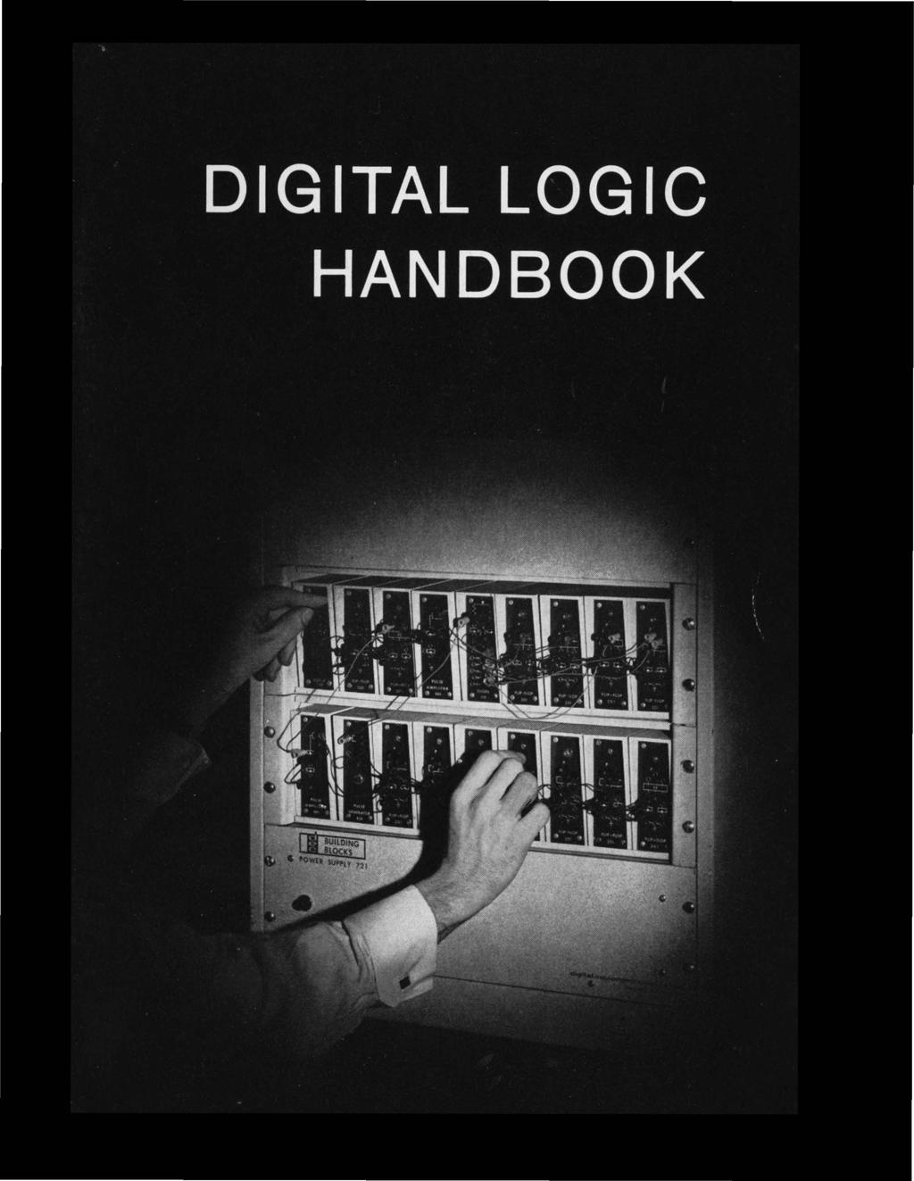
DIGITAL LOGIC HANDBOOK
|
|
|
- Magnus Lang
- 6 years ago
- Views:
Transcription
1
2 DIGITAL LOGIC HANDBOOK
3 COPYRIGHT, 1961, BY DIGITAL EQUIPMENT CORPORATION First Edition - September, 1960 Second Edition - November, 1960 Third Edition - March, 1961 PRINTED IN THE UNITED STATES OF AMERICA
4 INTRODUCTION DEC Digital Modules are a coordinated set of digital circuits used for building and testing computer systems. For use as laboratory equipment, they are packaged for convenient patch cord interconnections. For use in systems, they are packaged in a unique plug-in unit construction. They are available in three compatible speed ranges with maximum frequencies of 500 kilocycles,s megacycles, and 10 megacycles. DEC Modules are designed to be easy to understand and easy to use. People with no knowledge of Boolean algebra can perform logical design with DEC Modules, and those who like to use Boolean mathematics can very quickly and easily implement their equations. Straightforward static logic is employed, and only a small number of Modules is needed for most systems because of the high driving capability of each unit. The general logical principles utilized are the same for all Modules. The purpose of this booklet is to acquaint the reader with these principles. The logic used with DEC Modules is "static." "ONES" and "ZEROS" in this system are represented by two different DC voltage levels. The use of such a static system makes it possible to change the state of a system at any time. Logic is performed by the coincidence of levels which are sampled by pulses. Unlike "dynamic" logic, where ONES and ZEROS are represented by the presence or absence of a train of pulses, static logic is not tied to a fixed clock frequency and usually avoids precise timing problems. The rules governing loading will depend on the speed range of the equipment used. The rules and illustrations in this book are applicable principally to 500 kilocycle and 5 megacycle Modules. 3

5 DEC LABORATORY MODULES (TOP) AND DEC SYSTEM MODULES ARE AVAILABLE IN THREE COMPATIBLE FREQUENCY RANGES 4
6 CONTENTS INTRODUCTION.. DEC SYMBOLOGY BASIC DIGITAL MODULES The Transistor Inverter. Diode Logic. Flip-Flops. Delays.. Pulse Amplifiers Clocks... Pulse Generators. TYPICAL APPLICATIONS Counters... Parallel Adders Comparators Synchronizers Subtracters. Gray-to-Binary Code Converter RULES AND DEFINITIONS Inverter Usage Loading Definitions Marginal Checking. Indica tors.... BOOLEAN ALGEBRA. DEC TECHNICAL BULLETINS
7 DEC SYMBOLOGY A small rectangle with an enclosed solid triangle is an inverter. 1 tlector Base Input Emitter INVERTER A resistor with a large solid dot is a standard DEC clamped load resistor. CLAMPED LOAD The solid diamond is a logic level for which the assertion level is -3 volts. LEVEL-NEGATIVE The open diamond is a logic level for which the assertion level is ground. LEVEL-GROUND The solid arrowhead is a negative pulse (from ground). PULSE-NEGATIVE The open arrowhead is a positive pulse (from ground). r PULSE - POSITIVE Arrowheads (or diamonds) are used at all branch points to indicate signal flow. 6
8 BASIC DIGITAL MODULES THE TRANSISTOR INVERTER Most logical operations with DEC Modules are performed with saturating PNP transistor inverters. When a junction transistor is turned completely on or "saturated," the collector is practically a short circuit to the emitter of the transistor. If the emitter is at ground in this condition, the output from the collector will also be at ground voltage. When a junction transistor is turned completely off or ~~opened," the collector-to-emitter path is practically an open circuit. If the collector is connected to a clamped load resistor, the collector will be at -3 volts. Input O-~/V'\-+-+-f - 3v -15v W I I I Output + 10v FIGURE 1. I 1 ~ C'~::..d I I -i T'M""", ~ Inverter I I I 1 FIGURE 2 Figure 1 is a schematic drawing of a DEC inverter and clamped load resistor. The capacitor shunting the input resistor is used to provide overdriving current to the transistor during input level changes, thus switching the transistor much more rapidly. The resistor to +10 volts biases off the transistor to protect against noise voltage. The load resistor is clamped to -3 volts with a diode so that, when the transistor is off, the output signal is always at -3 volts regardless of the loading on the inverter output. 7
9 To simplify logic drawings, the symbology of Figure 2 is used. When the input is negative, the output is ttshorted" to ground. When the input is positive or at ground level, the transistor is open circuit~d and the output, if connected to a clamped load resistor, is at -3 volts. Input 1----<> Output FIGURE 3 The inverter switch is analogous to the mechanical switch, as shown in Figure 3. The logical designer can often build networks of inverters in the same manner as he would if he were using mechanical relays or simple switches. A B c FIGURE 4 FIGURE 5 Figure 4 shows three mechanical switches connected in a series to form an "AND" circuit. All switches A and Band C must be closed in order to ground the output. Similarly, in the series inverter network of Figure 5, all transistor inputs A and Band C must be negative in order to short the output to ground. If any input in Figure 5 is ground, that transistor will be an open circuit, and the output will be -3 volts. Therefore, the network also acts as an "OR" circuit for ground levels. 8
10 If any of the switches of Figure 6 close, the output will be shorted to ground. If A or B or C in Figure 7 is negative, the output will be shorted to ground. Only if all inputs are at ground will the network output be negative. The parallel arrangement in Figure 7 is an OR gate for negative levels and an AND gate for ground levels r--<> output r 1 r c FIGURE 6 FIGURE 7 Inverters can be stacked in complicated series-parallel combinations, like that of Figure 8, to perform sophisticated logical operations. There are some rules, however, since the inverters are not quite ideal switches. These rules are discussed in the sections beginning on Page 41. C B A ~-G G H=C+(B+A D) (E+F)-G H=C' [B'(A+D)+E'F+ G] FIGURE 8 DIODE LOGIC All logical systems could be constructed using only parallel and series combinations of transistors in inverter networks. However, as the number of inputs to a particular gate increases, it becomes more economical to perform the gating action with diode gates. The 9

11 INTERIOR VIEW OF 5 MEGACYCLE LABORATORY MODULE LABORATORY MODULE MOUNTING PANEL SHOWING POWER CONNECTIONS AT THE BACK 10
12 outputs of diode gates are permanently connected to a transistor inverter which re-establishes the reference level after every gate. Thus, DEC diode gates may be connected in tandem indefinitely. A o--i<l----r--i Bo--KJ--~ c o---ki--~ D o---ki---t E o--i<l---t F o---t< FIGURE 9 DEC negative diode units are six-input diodes tied to an inverter, as in Figure 9, so that anyone of the input terminals can turn on the inverter. This makes a six-input OR circuit for negative levels or pulses because A, B, C, D, E, or F can turn on the inverter and "short circuit" its output. This, of course, also acts as an AND circuit for ground levels. Bo---Dl---t c o---i>i---t Do---I>I----t E o---dl---t Fo--OI-~ FIGURE 10 The positive-type diode circuit, Figure 10, provides an AND circuit for negative levels and an OR circuit for ground levels. This unit is available only in DEC System Modules because DEC Laboratory Modules are usually employed in small systems and the economy resulting from the use of this type of unit is small. 11
13 FLIP-FLOPS If two grounded inverters are interconnected, as in Figure 11, a bi-stable ((flip-flop" is obtained. When one side is cut off, its output is negative. This holds the other side on, which, in turn, holds the first side off. FIGURE 11 If a grounded inverter A is connected to the off side B of the flipflop in Figure 12, the state of the flip-flop can be changed by pulsing the base of transistor A with a negative signal. This extra transistor will short the collector of transistor B to ground and will cutoff transistor C, which will turn on transistor B. The flip-flop will then stay in that state even after the signal is removed from A. input FIGURE 12 Simple flip-flops, such as in Figure 12, can be used wherever the load on the output is light and economy is important. DEC System Modules Types 1213 and 4213 contain circuits similar to this one. For general applications, it is desirable to have flip-flops with very low output impedance so that they can drive many other circuits. For this reason, most DEC flip-flops have buffer amplifiers on each side of the flip-flop. 12
14 FIGURE 13 A simple network is placed between the flip-flop in Figure 13 and the output amplifiers, which delays the change in the output. When the flip-flop is changed with a standard pulse, this delay is long enough so that the output does not change until after the pulse is over. This allows flip-flops to be sensed while they are being pulsed, which makes shift registers, counters and adders relatively simple. FIGURE 14 The symbol for a flip-flop is shown in Figure 14. In order to set the flip-flop to the desired state, the inputs at the bottom are ((shorted" through inverters to ground. When the input on the ZERO side has been shorted to ground, the ZERO output is set to the - 3 volt level and the ONE output is at ground. This is defined as the ZERO state. Similarly, when the flip-flop is in the ONE state, the ONE output is at - 3 volts and the ZERO output is at ground.... _Pulse Input Level Input FIGURE FIGURE 16

15 Flip-flops are always changed by momentarily shorting an input to ground, as shown in Figure 15. The input to the inverter is a DEC Standard Negative Pulse of 2.5 volts amplitude relative to ground. To gate information into a flip-flop, two inverters can be connected in series, as in Figure 16. If the level input is at ground when the upper inverter is pulsed, the flip-flop terminal will not be shorted to ground; but if the level input is at -3 when the negative pulse arrives, the input is shorted and the flip-flop is cleared. Since most DEC flip-flops have buffer amplifiers, it is permissible to use the buffer as the level gate. This added flexibility is useful since it allows reading into a flip-flop with only one inverter gate. I4--Pulse FIGURE 17 Figure 17 is a ~~jam transfer" gate employing DEC buffered flipflops. The contents of flip-flop A can be ~~jammed" into flip-flop B with a single pulse independent of the previous state of flip-flop B. The outputs of A are connected directly to the emitters of the pulse gates feeding the inputs of B. Both inverter pulse gates are pulsed simultaneously, but only the gate which has ground on its emitter will pass the pulse to set the flip-flop. For example, if flip-flop A holds a ONE, its ZERO output terminal will be at ground, allowing the right-hand gate to pass the pulse and set flip-flop B. FIGURE 18 The shift register of Figure 18 is another use of the jam transfer gate of Figure 17. Since the outputs of the flip-flops do not change until the shift pulse has passed, no logical delays are needed between flip-flops. 14
16 10 MEGACYCLE SYSTEM MODULE FLIP-FLOP SYSTEM MODULE MOUNTING PANEL WITH UNIT EXTENDER 15
17 When the inverters of Figure 19 are pulsed, the state of the flipflop will be changed or ~~complemented." On some of the DEC flip-flops this gating is done internally, and a complement terminal is brought out, as in Figure 20. L..&J~-Poise Complement Input FIGURE 19 FIGURE 20 There is also a complement output terminal P which will deliver a DEC Standard Negative Pulse every time the flip-flop complement input is pulsed. This P pulse output is useful in counters and adders. Input Pulse FIGURE 21 A typical counter arrangement using DEC complementing flipflops is shown in Figure 21. The pulses being counted enter on the right. They always complement flip-flop C and generate a standard pulse at P. This P pulse complements flip-flop B when flip-flop C 16
18 holds a ONE. When this P pulse gets through the gate and actually complements B, it will generate a P pulse out of B. The process is continued down the length of the counter. Only one inverter and one flip-flop are needed for each bit in the counter. Pulse FIGURE 22 System Module flip-flops also have direct clear and set terminals which allow flip-flop registers to be set or cleared without the use of pulse gates on each flip-flop. The input to these terminals is a DEC Standard Positive Pulse of 2.5 volts amplitude relative to ground. These pulses can be produced by DEC delays, pulse amplifiers, clocks, and pulse generators. Figure 22 shows a register being set to using the direct inputs. DELAYS DEC Delay units are flip-flops which have only one stable state. When the input terminal is ~~shorted" to ground by a Standard Pulse, the level output terminal will switch from its normal ground level to the -3 volt level for a fixed period of time, which is adjustable. A standard pulse will be produced at the pulse output when the level output returns to its normal a volt condition. The pulse output comes from a pulse transformer which has both terminals available. To obtain a negative pulse, ground the output from the positive terminal. To obtain a positive pulse, ground the output from the negative terminal. Pulse Input Level Output Pulse Output L-_~~+ Input Pulse Output - - ~ J -- c -- I Level Output t+t+ I'*t- ('--I-,U FIGURE 23 Typical waveforms for a delay unit are shown in Figure
19 FIGURE 24 Delay units are particularly useful in generating delayed standard pulses or signals of arbitrary width. The network of delays in Figure 24 will produce the waveform in Figure 25. FIGURE 25 PULSE AMPLIFIERS DEC pulse amplifiers are a powerful logical element because they not only amplify and standardize the shape of pulses but also gate pulses. When the same logical gating is to be done on a whole register of flip-flops, it often can be done once before the pulse amplifier drives the register. o"i Pulse 0... A;,.;,;,m_p...--O + FIGURE 26 The outputs of the pulse amplifiers come from pulse transformers, which have both terminals available so that either positive or negative pulses may be obtained, depending on which terminal is grounded. Positive pulses are used to direct set and clear flip-flops without inverters. Negative pulses are used for setting, clearing and complementing with inverters. 18
20 CLOCKS DEC clocks produce standard pulses from stable, variable frequency, RC-coupled oscillators which have a wide range of frequencies available. These clocks are often used as a primary source of timing for large systems. Where very precise timing is needed, crystal clocks which contain a single-frequency crystal oscillator are available. I Clock I ~ + FIGURE 27 PULSE GENERATORS DEC pulse generators are used to initiate action as a result of outside activity. Every time the input of these pulse generators goes more negative than -272 volts after having been more positive than -1 volt, a standard pulse is generated. Most outside actions can be converted into voltage levels that will fill this criterion. H :~~~e i -~ I + I ~1 I External '=' SWitch ~.J -15 FIGURE 28 It is difficult to generate a single pulse from a switch or relay closure because contacts bounce many times before they finally make a solid contact. If these are connected directly to a pulse generator, they will produce a pulse for each contact bounce. An integrating circuit is included which can be connected between the pulse generator and the contact. This circuit converts the many fast voltage changes into a single slow change, which generates a single pulse. 19
21 FRONT VIEW OF DEC SYSTEM MODULE MOUNTING PANEL SHOWING STANDARD PIN CONNECTIONS FRONT VIEW OF NEW TAPER-PIN MOUNTING PANEL WHICH PERMITS PATCHCORDING OF SYSTEM MODULES 20
22 TYPICAL APPLICATIONS COUNTERS Building a counter with DEC flip-flops is straightforward due to the built-in delay and the availability of the P pulse terminal. A carry pulse is created when the P pulse is fed to the base of a gate which is conditioned by the ONE state of the flip-flop. STRAIGHT BINARY COUNTING Pulses...-ToBe Counted FIGURE 29 STRAIGHT BINARY COUNTER (DEC Flip-Flops Type 201, 1201, 3201, or 4201) COUNTING SEQUENCE o When flip-flop D in Figure 29 is in the ONE state, its ZERO output terminal is ground. When it receives a complement pulse, the gate will pass a P pulse into the complement input terminal of flip-flop C. If flip-flop D had been in a ZERO state, the P pulse would have been prevented from complementing flip-flop C. The series connection of P pulses and gates is the high-speed carry chain. The carry propagate time per digit is much less than the flip-flop's total transition time. To assure that flip-flop D will not be in the process of changing state while flip-flop C is receiving its carry pulse, a delay has been built into each flip-flop package. This insures that the ONE and 21
23 ZERO output terminals will not change until after the carry pulse has been gated. Each bit of the counter requires one flip-flop and one transistor gate. There are two gates contained in each DEC Flip-Flop Type 201, 1201, 3201, and If DEC Laboratory Modules are used, the results can be read by means of the indicator lights on the front panel. DEC System Modules Types 1201 and 4201 are compatible with Indicator Drivers Types 1675 and 1669, which are suitable for driving remote indicator lights. SPECIAL COUNTS Often it is desirable to build a counter that will produce a signal after a particular number (N) of events have occurred. If N is an integer power of 2, the output is automatically produced by the final digit of a counter of appropriate length. If N is not a power of 2, gating must be performed to detect the desired number, generate a signal, and reset the counter to O. Pulses ~~_~I-- ~"",,_To Be Counted FIGURE 30 ARBITRARY COUNT - COUNT OF 12 ILLUSTRATED (DEC Flip-Flops Type 201, 1201, 3201, or 4201) 22
24 Transistor inverter gates or diode gates may be used to sense the number N-l, close the input to the counter, and re-route the Nth input pulse so that it will clear the counter and generate an output signal Although this is not always the optimum method, it is a completely general method which will work for any value of N. 4 0 Pulses To Be Counted COUNTING SEQUENCE o I FIGURE 31 COUNT OF 3 (DEC Flip-Flops Type 201, 1201, 3201, or 4201) A typical counting sequence is shown for N = 3 in Figure 31. The progress of the count is shown in the table. When the count of 2 is reached, the next pulse will clear the counter and generate an output signal. Count of 3 Count Of Jl, " ~---o r------o Pulses..-+-ToBe Counted COUNTING SEQUENCE o FIGURE 32 COUNT OF 6 (DEC Flip-Flops Type 201, 1201, 3201, or 4201) A counter for 6 is made from the counter for 3 by preceding it with a binary counter (Figure 32). Examination of the counting 23
25 sequence shows that the least significant digit alternates between ZERO and ONE, while the two most significant digits follow the same pattern as the count of 3. The circuit for flip-flops A and B is identical to that for the count of 3 except that two additional gates are necessary. These are required because the input to the countof-3 portion includes a conditioning level, as well as a pulse. BINARY CODED DECIMAL COUNTING Pulses To Be Counted COUNTING SEQUENCE o FIGURE 33 COUNT OF 5 (DEC Flip-Flops Type 201, 1201, 3201, or 4201) From the simple count-of-5 circuit, binary coded decimal counters may be generated. Count of ~ Count Of 2 Pulses To Be Counted COUNTING SEQUENCE o FIGURE 34 BINARY CODED DECIMAL COUNT OF 10 - (DEC Flip-Flops Type 201, 1201, 3201, or 4201) 24
26 To give a count of 10) the counter for 5 is preceded by a binary counter (Figure 34). This circuit is compatible with DEC's BCD Decoder and Light Driver Type 1671, which has 10 output lines for driving a decimal output display. A counter for 100 can be made by cascading two BCD stages. Because the complement input to A is used only at the time the decade is cleared, the P pulse can feed the next stage without being gated. Any number of BCD stages may be cascaded in a similar manner. Up COUNTERS AND DOWN COUNTERS ARE AMONG THE LOGICAL OPERATIONS WHICH CAN BE PERFORMED WITH THE DEC BASIC LOGIC KIT 25
27 DOWN COUNTERS Pulses To Be Counted Down FIGURE 35 DOWN COUNTER (DEC Flip-Flops Type 201, 1201, 3201, or 4201) In a down counter, each successive pulse will decrease the count by 1. The method for building a down counter is essentially the same as that used in the up counter, except that each flip-flop input is conditioned by the ZERO state of the previous flip-flop. In this way, the P pulse chain will form a high-speed borrow circuit instead of a carry circuit. Counter Has Overflowed Counter Has Gone Negative FIGURE 36 BINARY UP-DOWN COUNTER (DEC Flip-Flops Type 1201 or 4201) 26
28 An up-down counter combines the techniques found in the individual up and down counters. This is made possible by use of DEC Flip-Flops Type 1201 or Each of these units contains a flip-flop with two independent sets of complement and associated P pulse terminals. Thus, it is possible to connect one set to form a high-speed carry circuit, while the other set forms a high-speed borrow circuit. Of course, the add and subtract pulses should not be allowed to arrive simultaneously MEGACYCLE COUNTING Pulses... -ToBe Counted FIGURE Me BINARY COUNTER (DEC Flip-Flops Type 5201 or 6201) The logic behind a 10 megacycle counter is the same as that for a 5 megacycle or 500 kilocycle counter; however, the loading rules differ. Two inverters are required for each bit. The pulse must go to the lower inverter, as shown, to insure sufficient pulse gain to propagate the carries. Only one 10 megacycle flip-flop is needed for counting at 10 megacycles where carry propagate time is not important. Such a mixed system is shown in Figure 38. In the transition from one type of equipment to another, a pulse amplifier with feedback is required to lengthen the pulse. PARALLEL ADDERS Addition of the contents of the incident number register to the contents of the accumulator is accomplished in two discrete steps, a half-add and a carry. This is made possible by using DEC Flip-Flops Types 1201 or 4201 as in Figure 39. These units have two discrete complement inputs, each with its own P pulse terminal. The first step is half-add. Each digit of the accumulator is complemented if the corresponding digit of the incident number is a ONE. 27
29 KC BLDG. BLOCKS Series 3000 or MC BLDG. BLOCKS Series 100 or 1000 o PA 5 MC 70 NS Pulses 10 MC 40 NS Pulses FIGURE MC COUNTER, MIXED SYSTEM - SHOWING PULSE STRETCHING (Lower cost than Figure 37 counter, but longer propagate time)
30 Carry ~------~' T ~~ (Step2) Carry to Next ~ ~_--1_..., Stage, or End Around Carry End Around Carry,(, Add (?tep 1) FIGURE 39 PARALLEL ADDER (Accumulator Flip-Flops DEC Type 1201 or 4201)
31 The second step is carry. A carry will be generated if a digit in the accumulator is ZERO and the corresponding incident number digit is ONE. A carry will be propagated if an accumulator digit is ONE and it also receives a carry pulse from the next less significant accumulator digit. After the carries have propagated, the contents of the incident number register may be modified to add another number to the accumulator. Table I provides some examples. I Original Incident Accumulator Accumulator Accumulator Number Number I After Half-Add After Carry TABLE I MEMORY CORE EVALUATOR MADE FROM DEC LABORATORY MODULES 30
32 Variations of this technique can be used to make a subtracter, a multiplier, a divider, etc. A faster adder can be built by using 10 megacycle Flip-Flops Type 6202, as shown in Figure Carry Carry to Next (Step 2) Stage. or End Around Carry End Around Carry Incident Number Register FIGURE 40 PARALLEL ADDER USING 10 Me FLIP-FLOPS (Accumulator Flip-Flops DEC Type 6202) COMPARATORS COMPARING A TOGGLE SWITCH REGISTER AND A FLIP-FLOP REGISTER The simplest comparator is the type used in building a counter which will stop or reset itself after a preset number of counts. This type of comparator, as illustrated in Figure 30, consists merely of a string of diode gates with each diode connected through a toggle switch to a flip-flop. Each toggle switch corresponds to a single binary bit, with a closed switch representing a ONE and an open switch representing a ZERO. Since opening a toggle switch has the same effect as removing the corresponding diode, there may be several numbers which would generate a comparator output. However, the first comparator output will correspond to the desired number if the counter always begins in the all ZERO state. This, of course, requires that the counter be reset, or the counter input be terminated as soon as the comparator output appears. The comparator output, in Figure 30, is used to close the counter input and re-route the next count pulse to perform the clearing action. Since this action requires an additional input pulse, the toggle switches must be set to detect one less than the desired number. 31

33 This technique can also be used with a down counter. The diode gates are then connected to the flip-flops so that a closed switch corresponds to a ZERO. The first comparator output is used to preset the counter to the all ONE state or to turn off the counter input. Comparing a toggle switch register with an arbitrary flip-flop register requires a single-pole double-throw switch for each bit. Thus both ZEROS and ONES are detected. COMPARING Two FLIP-FLOP REGISTERS Comparison of two flip-flop registers requires an "EXCLUSIVE OR" for each corresponding pair of bits, since there are two possible conditions which will produce an inequality; i.e., bit Ai = 0 and Bi = i or Ai = i and Bi = o. The entire set of EXCLUSIVE OR'S must then be or'd together to determine when any pair of bits is unequal. Figure 41 shows an example of a two-register comparator. The EXCLUSIVE OR'S consist of two inverters. The final oring function is accomplished by simply tying the inverter outputs together. Whenever the two bits of any pair are different, the comparator output will be at ground. When there are no differences, the output will be negative. B1 (0) B1 (1) B2(0) B2(1) BN(O) BN(1) FIGURE 41 COMPARATOR (10 me, 5 me or 500 kc Inverters) Of course, there is a limit to the number of inverters which can be connected in this manner. If a single standard clamped load resistor is used to define the -3 logic level, then the maximum number of "on" bases is six (as explained in the section entitled "Loading Definitions" and the technical literature describing the inverters). Since only one base in each EXCLUSIVE OR pair can be "on" at a time, the maximum configuration is actually seven pairs of inverters. 32
")
34 To increase the allowable number of inverters, the clamped load resistor may be replaced by a 10,000 ohm resistor externally wired to the -15 volt terminal. The maximum configuration is then 14 pairs of inverters; however, the output can drive only one inverter base. Unequal Y1(1) X_1 (.;...;.1)..f>IoI~ Y1(O) FIGURE 42 COMPARATOR (DEC Diodes Type 4113) Figure 42 shows an equivalent comparator with the inverters replaced by two-input diode units. Here the load determining factor is the ico of the transistors. If only one unit Base Load is to be supplied by the output, then up to 100 pairs of diode gates may be used. If the number of pairs of diode gates is decreased, then the output driving ability is increased proportionally. SIGN OF AN INEQUALITY A more sophisticated comparator is used to compare the numerical value of two registers to determine equality or the sign of an inequality. This problem requires that each pair of bits be investigated in the order of their significance. Once an inequality has been discovered, all further investigation must be stopped so that the differences in bits of lesser significance will not affect the output. Figures 43 and 44 show the i th stage of such a comparator chain. To begin investigation, the equality line is brought to -3 volts. This negative signal is ANDed with an EXCLUSIVE OR for the first pair of bits. If there is equality, then the negative signal will propagate down the equality line. If all corresponding pairs of both registers are equal, the negative signal will appear at the end of the final stage. However, if an inequality is reached, further investigation will be stopped and the equality line output will remain at ground. If this inequality is such that register A is greater than register B, then a ground signal will be generated at the sign output. 33
35 Equality Line Equality Line From Previous Bits -3 Volts Indicates Equal So Far ALeO) BteO) t AW) Bt(O)--n..., -----'--~ (0 Volts Indicates A>B) Equal So Far Meaning of Outputs Sign Equality Output Output Meaning -3-3 A=B -3 0 B>A 0 0 A>B 0-3 Impossible FIGURE 43 COMPARATOR (DEC Diodes Type 1111 or 4111) Equality Line From Previous Bits - 3 Volts Indicates Equal At (1) So Far --D... ~"... -K... -Al(O) Bt (1)... CI--BtCO) t At (1)--I)... ~ Bl(O)--I)... Sign Output (0 Volt Indicates A>B) Meaning of Outputs Sign Equality Output Output Meaning -3-3 A=B -3 0 B>A 0 0 A>B 0-3 Impossible FIGURE 44 COMPARATOR (DEC Diodes Type 4113) There is no limit to the number of stages through which the equality line may propagate. The restrictions on the sign output are similar to those described in the previous section. In Figure 43 the sign output is fed by diode units with grounded emitters. Thus, the output will drive one unit base load if it is fed by one clamped load resistor and up to 100 diode gates. 34
36 With the configuration for the sign output as shown in Figure 44, it may be necessary for a single "on" transistor to supply the base current for other transistors with both negative bases and emitters. If a standard clamped load resistor is used to define the output level, then a maximum of seven inputs may be connected. If the clamped load resistor is replaced by a 10,000 ohm resistor wired to the -15 volt terminal, then the maximum number of inputs is 14. PARITY GENERATOR A Parity Generator is a comparator which compares flip-flops within the same register. The circuits shown in Figures 45 and 46 are made up of EXCLUSIVE OR'S as in the previous examples. Each EXCLUSIVE OR determines whether the sum of its two inputs is odd or'even. The circuits are built up in a pyramid arrangement so that the output of the final EXCLUSIVE OR gives the parity of the sum of all the inputs. X2(O) X2(1) X4(O) X4(1) X6(O) X6(1) X8(O) X8(1) FIGURE 45 PARITY CIRCUIT (5 me or 500 ke Inverters) To lighten the load on the inverters, 10,000 ohm resistors are used instead of standard clamped load resistors. The maximum series configuration is three inverters or one inverter and one 2-input diode gate. When the emitter of an inverter is driven from a flip-flop output (Figure 45), the flip-flop must be counted as an inverter. 35
37 _-<>Odd r "'T'" ~Even X 2(0) X2(1) X4(Q) X3(O) ~t= X4(1) FIGURE 46 PARITY CIRCUIT (DEC Diodes Type 4113) SYNCHRONIZERS Synchronizers are extremely important in any digital system, not only to determine what will happen if two asynchronous or incompatible signals occur, but also to assure that catastrophic errors will not result from such signals. Asynchronous signals are often commands such as start, stop or clear. Incompatible signals must be guarded against whenever a single flip-flop register is connected for more than one possible mode of operation. Some typical cases where synchronizers are required are as follows: 1. Shift Registers - When a shift register is being changed from parallel mode to serial mode or vice versa, care must be taken that a split or partial pulse is not allowed to enter the system. Such a pulse could result in a partial shift, partial read-in or partial read-out. Likewise, a bi-directional shift register should never be commanded to shift left and shift right at the same time. 2. Counters - Particular care must be taken with start or stop signals which occur at random times relative to the counter input. If a synchronizer is not used, this situation might result in a split or partial pulse which would enter the system and propagate only part way down the carry chain. Thus, the entire number in the counter, or any part of that number, could be wiped out. A similar split pulse might occur in a bidirectional counter if the add and subtract inputs were pulsed simultaneously. 36
38 Basically, a synchronizer is accomplished by ANDing together a random input signal and a primary pulse stream (usually a clock) and feeding the results of this AND gate into a single flip-flop. If the random signal arrives while the clock pulse is occurring, the single synchronizer flip-flop makes the decision as to whether the signal will be accepted or rejected. Provision must also be made for the rejected signal to be accepted by the next clock pulse; thus, the input signal may be slightly delayed by the synchronizer flip-flop, but there will be no "middle" state which would activate only a portion of the main circuit. LEVEL SYNCHRONIZER Figure 47 shows a method of synchronizing a command level, such as a mode control, with a primary pulse stream. When the input level is ground, the primary pulse stream will pass through terminal A. When the input level is negative, the primary pulse stream will pass through terminal B. If the input level is in the process of changing at the time the clock pulse occurs, then the decision to accept or reject the signal change will be made by the synchronizer flip-flop only. Thus, no pulses will ever pass out both terminal A and terminal B, and no split pulses will ever pass out either terminal. This method, or a variation, is often used in controlling the direction of count in an up-down counter. PA PA Output A Output B Clock I"put ~ Level ' ' Clock Output A Output B Input Level FIGURE 47 LEVEL SYNCHRONIZER (DEC Flip-Flops Type 201, 1201, 1209, 3201, 4201, or 4209) 37
39 START-STOP SYNCHRONIZER Figure 48 shows a method for synchronizing start and stop commands with a primary pulse stream. This type of synchronizer is extremely important in counters which are used to measure time intervals. PA Output Stop,t Pulse V Output ----.I FIGURE 48 START STOP SYNCHRONIZER (DEC Flip-Flops Type 201, 1201, 1209, 3201, 4201, 4209, 5202, or 6202) The random start and stop pulses will be converted to stop or start levels by flip-flop A. Flip-flop B will convert this randomly changing level into a level that changes synchronously with the primary stream. This level, in turn, conditions the output pulse stream. The action may be delayed by one clock pulse. However, a split pulse will never be allowed to enter the main system. SINGLE PULSE SYNCHRONIZATION Figure 49 shows a method for synchronizing a single pulse with a primary stream of pulses. The operation of the synchronizer is similar to that of Figure 48 except that the stop command is autorna tically genera ted by the first pulse to leave the synchronizer. Thus, one, and only one, pulse will pass into the main system, and this pulse will be synchronized with the main system. 38
40 Output T~i~I~:r Clock V Output-----v FIGURE 49 ONE PULSE SYNCHRONIZER (DEC Flip-Flops Type 201, 1201, 1209, 3201, 4201, or 4209) SUBTRACTERS An adder may be used for subtraction as well as addition. To subtract a number from the accumulator, the number is made negative and added to the accumulator. The steps involved in performing a subtraction depend on whether the ~~one's complement" or the ~~two's complement" number system is used to represent a negative number. The ~~one's complement" number system is easiest to implement. To subtract a number from the accumulator, the steps are: (1) complement the incident number, (2) half-add, and (3) carry. With this number system it is necessary to implement an ~~end-around carry" from the most to the least significant digit. This connection is shown in Figures 39 and 40. Subtraction is performed in DEC's PDP computers by (1) complementing the accumulator, (2) half-add, (3) carry, and (4) recomplementing the accumulator. GRAY-TO-BINARY CODE CONVERTER A frequent problem in digital control work is to convert a Gray coded number, such as a shaft position, into a pure binary number so that it can be used conveniently in arithmetic operations. The DEC converter begins examination with the most significant bit and proceeds down the line, making use of two basic conversion principles: (1) the most significant digit is identical in Gray and binary and (2) if a digit is a 1 after being converted to binary, the following digit is complemented. 39
41 The DEC converter does not require any shifting or transferring of information. All logic is done by means of inverter gates, arranged in such a way that the convert pulse will simultaneously convert all digits from Gray to binary. Conv_e...;,rtoof- --t_-+i FIGURE 50 GRAY-To-BINARY CONVERTER (DEC Flip-Flops Type 201, 1201, 3201, 4201, 4209, 5202, or 6202) 40
42 RULES AND DEFINITIONS INVERTER USAGE 5 MC AND 500 KC MODULES DEC transistor inverters serve two functions. When used as level gates, they are placed in series and parallel configurations to perform logic. When used as pulse gates, the inverter will sample the logic performed by the level gates and read the results into a flip-flop or other active element. When used as a pulse gate, an inverter will drive one and only one pulse unit. Inverters serving as level gates are usually considered as simple switches when designing logical networks, but because they are not ideal switches, there are certain limitations which have to be taken into account. The voltage drop across saturated inverters is not zero; it is closer to 0.1 volt. As a result, inverters cannot be stacked indefinitely. Three inverters is the maximum which can be put in series if the output is to drive another inverter, as in Figure 51. FIGURE 51 FIGURE 52 If inverters are in series with the output of a flip-flop, as in Figure 52, the flip-flop buffer inverter is considered to be one of the three allowed series transistors. When the output of a series of inverters is driving the input of a pulse amplifier or delay unit or the set or clear input of a flip-flop, as in Figure 53, a fourth transistor serving as a pulse gate may be added in series. Only three may be used in series when driving the complement input of a flip-flop. It is important to note that a clamped load resistor is tied to the emitter of each pulse transistor when it is being driven from an inverter or a network of inverters, as in Figure
43 FIGURE 53* Because inverters are not really ideal switches, each collector of a series string of DC inverters supplying a pulse inverter will go somewhat negative during the pulse. This means that, if a series of inverters is supplying both pulse current and a DC signal, care must be taken because a signal will occur in the DC output during the pulse. Pulse FIGURE 54 In Figure 54, when the input C is negative, flip-flop A should be set by the pulse, but flip-flop B should not be set. However, during the pulse, collector E of the DC inverter feeding flip-flop A will go slightly negative. It will partly turn on the DC inverter feeding flip-flop B, and sometimes it will set flip-flop B as well as flip-flop A. This network will work only if the pulses are not simultaneous. *The clamped load resistor is not needed in 5 megacycle circuitry when the pulse inverter is driven from a single series of inverters and the length of wire between inverters is short. In the 500 kilocycle line this clamped load resistor can be replaced by a IN276 diode from the emitter of the pulse inverter to ground, connected so as to prevent this point from going positive. 42
44 CONSTRUCTION OF DIGITAL SYSTEMS, SUCH AS THIS DEC MEMORY TESTER, Is GREATLY SIMPLIFIED BY THE USE OF SYSTEM MODULES MOUNTING PANELS MAY BE PRE-WIRED TO FORM SYSTEM SUB-AsSEMBLIES 43
45 FIGURE 55 The network shown in Figure 55 will work whether or not the pulses are simultaneous. Two additional inverters have been added so that collector E will no longer be pulled negative by the pulse, since the pulse current will now come directly from ground instead of collector E. (If both outputs are feeding the same flip-flop, the network shown in Figure 54 can be used safely because the output of the A side will be much greater than that of the B side.) LOADING DEFINITIONS To facilitate the design of systems, a number of simple loading definitions and rules have been made. These do not cover all possible configurations, but they do serve as a useful guide. A "BASE LOAD" is the current which must be taken from the base of a DC inverter to keep it in a saturated state. In this condition the inverter base input terminal is at -3 volts, the transistor base is at ground, and 1 rna current is drawn through the 3000 ohm base resistor. Inverter load resistors, when clamped at -3 volts, have about 12 volts across their 1500 ohms, and they can accept about 8 milliamperes of current. Ideally, this would drive 8 units of BASE LOAD, but tolerance considerations limit the number to 7. A "PULSE LOAD" is the load presented to a pulse source when driving the base of an inverter. Pulse amplifiers are usually limited to driving 16 pulse bases. This number should be decreased if the bases are widely separated, and it can be increased to 18 if they are all close together. The 44

46 series inductance and shunt capacity of the connecting wires can make the pulses at the end of a string of bases either large or small. Consequently, when a number near the maximum is being driven, the pulse amplitude should be carefully checked after installation. A terminating resistor in the loo-to-300 ohm range is desirable to reduce ringing on a heavily loaded pulse line. A "PULSE LOAD" is also the load seen by a pulse source when driving one direct set or direct clear input of a flip-flop. The loading on a pulse source is approximately the same as when driving a base. One pulse source, of course, cannot drive both direct inputs of flipflops and inverter bases because the direct input pulses are positive from a normal ground level and base input pulses are negative from a normal ground level. A "PULSED EMITTER LOAD" is the load seen by the collector of an inverter driving the pulse input to a flip-flop, pulse amplifier or delay. The pulse current goes through all the inverters in series with the pulse input, and it should be assumed to be the load on each of the series inverters. A "DC EMITTER LOAD" is a load seen by the collector of an inverter driving a clamped load resistor. This load is also seen by the collector of an inverter which is driving an emitter in a network of inverters which is terminated by a clamped load resistor. FIGURE 56 The collector of an inverter driving an emitter in a network of transistors must also supply the base current leaving the inverters higher in the chain. This number is normally small, but in complex networks it must be considered. An inverter can drive no more than one clamped load resistor and six bases of ~~on" inverters. Since transistors are almost symmetrical, this ~~on" base current can also flow through the collector of a transistor whose emitter is open, as shown in Figure 56. In this case, the collector of the bottom ~~on" transistor must carry the current A from the load resistor and the base currents from B, C and D. 45
47 , DEC POWER SUPPLIES PROVIDE PROPER VOLTAGES FOR LOGICAL OPERATIONS DEC HIGH CURRENT PULSE EQUIPMENT INCLUDES NEGATIVE AND POSITIVE CURRENT DRIVERS AND CURRENT CALIBRATORS 46
48 MARGINAL CHECKING Marginal checking is used in a system to find the margin of safety between the condition of a system and the point of failure. Marginal checking is normally used in routine maintenance to find deteriorating components before they cause system failure. In many instances routine marginal checking is not necessary due to the long life of modern transistors, but it is still invaluable in debugging a new system. Without marginal checking, a system may be assembled with a number of mistakes which do not cause failure but which do not provide the system with as much margin as it should have. In systems made with DEC Modules, the + 10 volt bias on inverters is varied for marginal checking. In most Modules, the + 10 inputs are broken into two groups to make possible most critical marginal checking. In large systems, like the DEC Programmed Data Processor, the +10 lines to the Modules are broken down into several groups so that small portions of the system can be marginal checked at one time. If the inverter transistor has marginal gain, it will fail when the + 10 supply is increased less than 5 volts because the drive to the base of that transistor is lessened. Reducing the positive bias on an inverter will detect noise on the inverter input or a condition where the input does not come sufficiently close to ground. Normal margins on a system are plus and minus 5 volts on the +10 volt supply. INDICATORS In most systems an indicator lamp is connected to each flip-flop to show its logical state. In DEC Laboratory Modules the indicator lamps are built into the flip-flop units with their own transistor drivers. Types 1669 and 1675 plug-in units are used to drive indicators with the System Modules. The indicator drivers are power transistors in an inverter circuit, very much like a logic inverter except that the 3000 ohm resistor in the base is not bypassed with a capacitor. In the high-speed lines, the 3000 ohm resistor is included in the flip-flop package and not in the 1675 package to avoid capacitive loading on the flip-flop output. However, in the low-speed line the base resistors are included in the 1669 package. The load of the inverter is the incandescent lamp, which is tied to the -15 supply. When the inverter is on, the full 15 volts is across the lamp bulb. Normally, a GE 327 aircraft-type indicator 47
49 lamp bulb is used. This is a conveniently small bulb with very good life characteristics. It is rated at 24 volts, but when operated at 15 volts the light output is pleasant, and the life of the lamp is very long. The DEC Type 1671 BCD Light Driver is designed to drive a decimal display from either a binary coded decimal register or a Gray coded decimal register. This unit decodes a decade (four flip-flops) into ten lines and amplifies the output. The output will produce up to 150 milliamperes at -20 volts. This is sufficient for a GE 47 lamp, such as those used in the Industrial Electronic Engineers Model decimal display unit. 48
50 BOOLEAN ALGEBRA NOTE: As mentioned in the Introduction, a knowledge of Boolean algebra is not a prerequisite to the performance of logic design with DEC Modules. However, Laboratory Modules and System Modules can be used to implement Boolean equations quickly and easily. Boolean algebra was introduced in 1847 by an English mathematician, George Boole. The purpose of the algebra was to find a shorthand notation for the system of logic originally set forth by Aristotle. Aristotle's system dealt with statements which were considered to be either true or false, but never partially true or false. Boole's algebra was based on a single valued function with two discrete possible states. Boolean algebra lay almost dormant until recent times. Today, however, it is gaining widespread recognition as an efficient method for handling any single valued function with only two possible states. When it is applied to binary arithmetic, the two states are ZERO and ONE. When discussing a switch, the two values are OPEN and CLOSED.! =0 r I =1 FIGURE Bl The convention used will be that the OPEN state corresponds to the ZERO state while the CLOSED state corresponds to the ONE state. 49
51 OR FUNCTION n C y A +B= C 0+ 0= = = = 1 FIGURE B2 If two switches, A and B, are connected in parallel to form a gate, inspection shows that the gate can only transmit information if A or B or both are in the transmitting state, i.e., CLOSED. This is written in equation form as A +B =C (A or B equals C) Figure B2 shows the parallel combination of two switches along with its equivalent inverter gate and a table giving the value of C for all possible values of A and B. B C = C = B C ~ (A+B)+ C = A+(B+C) A+B+C FIGURE B3 By adding a third gate in parallel, as in Figure B3, it becomes obvious how the OR function may be extended to any number of variables. This figure also serves to illustrate that the commutative and associative laws are valid for the OR function, i.e., A+B=B+A (A + B) + C == A + (B + C) == A + B + C 50
52 AND FUNCTION Q AB= C 00= 0 01= 0 1 0= = 1 FIGURE B4 If two or more gates are placed in series, the result is known as an AND gate. Inspection of the arrangement in Figure B4 shows that the resulting gate will transmit only if both A and Bare CLOSED, i.e., equal to ONE. The equivalent equation in Boolean form is AB =C (A and B equal C) A(BC) _ ABC _ C B A FIGURE B5 Figure B5 demonstrates how the AND function is applied to more than one variable. The commutative and associative laws also hold. AB =BA A(BC) == (AB)C == ABC 51
53 IDENTITIES! 0 ~A ~A A Y A r r 1+A=1 O+A=A 1A=A OA=O \ y n c \B \c y y A (B+C) = AB+AC FIGURE B6 To enable the simplification of Boolean functions, there are many identities which are helpful. In Figure B6, the combinations of switches and corresponding equations demonstrate these identities. COMPLEMENT If two gates are connected so that the same signal will open both of them or close both of them simultaneously, then the switches are given the same symbol. If two gates are connected so that a single signal will open one gate while closing the other gate, and vice versa, then these gates are said to be the complement of each other. Thus, if one gate is labeled A, the other gate will be labeled A (read Unot A"). 52
54 if An entire function may also be complemented. For example, then C = ACB + C) C = A(B + C) The use of one label for more than one gate makes the following identities helpful: A+A=A A+A=l A=A AA = A AA = 0 DE MORGAN'S LAWS Two unique laws which can be applied only to Boolean algebra are known as De Morgan's laws. A + B + C N = ABC... N ABC... N = A + ii + C N These laws may be verified by constructing a table of various possible values. BOOLEAN ALGEBRA FOR USE WITH VOLTAGE LEVELS Since DEC voltage levels have only two possible values, Boolean algebra can also be useful in the study of these levels. A FIGURE B7 The basic unit of DEC Logic is the transistor inverter. The simplest use of the inverter is to perform a complement. If the emitter is at ground and a signal is applied to the base, the resulting output is the complement of the base input. 53
55 ABC D E F Negative Or Gate A+B+C+D+E+F=G ABC D E F Negative And Gate ABCDEF=G FIGURE B8 A simple OR gate is formed by means of diodes, as shown in Figure B8. If A or B or C or D or E or F or any combination of these is negative, the resulting output is negative. A similar unit with the diodes reversed will form an AND gate. Only if A and Band C and D and E and F are negative will the resulting output be negative. Inspection of these diode units shows that the AND and OR gates will be interchanged if the levels are defined in the opposite manner. That is, if ground is defined as a ONE and negative is defined as a ZERO. This is a demonstration of De Morgan's law. A c A_-<>I c B And Gate AB=C FIGURE B9 B Or Gate A+B=C If the signals are manipulated without the encumbrance of a permanent sign convention, the same gate may perform many functions. Figure B9 shows an inverter which serves as an AND gate if the following definitions are used: A = 1 if negative, B = 1 if ground, C =1 if ground. The same transistor can be used as an OR gate if the opposite definitions are made, i.e.: A = 1 if positive, B = 1 if negative, and C = 1 if negative. For this reason, DEC uses the sign convention that the diamond arrowheads on signals indicate the required polarity for the desired action. A solid diamond denotes a -3 volt level for assertion, while a hollow diamond denotes a ground level for assertion. By using this method, it is possible to combine amplification and gating without added inversions as would otherwise be necessary. Several illustrations are shown in Figure BIO. 54
56 1"""" _-<::.. C A B A r-----~----~_4.c B A+B=C AB=C C A A A C B B B AB=C A+B=C C=AB+AB C=AB+AB FIGURE BIO 55
57 DEC TECHNICAL BULLETINS NOTE: DEC digital circuit packages are being renamed "Modules." As new bulletins are published, the two basic product lines will be referred to as "Laboratory Modules" instead of "Digital Test Equipment" and as "System Modules" rather than "System Building Blocks." DEC Building Blocks & Digital Systems (A-700B) - catalog listing DEC's complete product line.. short form DEC 10 Megacycle Building Blocks (A-710) - describes new 5000 Series Digital Test Equipment and 6000 Series System Building Blocks. de Expanded 100 Series DEC Digital Test Equipment (B-100) - scribes DEC's 5 megacycle patchcord units. New 3000 Series DEC Digital Test Equipment CB-3000) - DEC's 500 kilocycle patchcord units. describes Expanded 1000 Series DEC System Building Blocks (C-1000A) describes DEC's 5 megacycle plug-in units. New 4000 Series DEC System Building Blocks (C-4000A)-describes DEC's 500 kilocycle plug-in units. DEC Basic Logic Kit CE-150) -describes a basic selection of DEC Digital Test Equipment and Accessories which can be used to perform a variety of logical operations. DEC Programmed Data Processor (F-10) - describes DEC's PDP-1 high-speed, solid state, general purpose computer. DEC Memory Tester Type 1512 (F-1512A) -describes DEC's 1500 Series testers for coincident current core memories. DEC Memory Tester Type 1514 (F-1514) - describes DEC's 1500 Series testers for word address and coincident current core memones. DEC Automatic Memory Core Tester Type 2101 (F-2101)-describes DEC's automatic tester for ferrite magnetic memory cores. DEC Programmable Pulse Generator Type2104 (F-2104)-describes DEC's versatile new pulse generator system. DEC Memory Exerciser Type 2201 (F-2201) -describes DEC's exercisers for coincident current core memory systems. Copies of the above bulletins are available on request from the DEC Sales Department, 146 Main Street, Maynard, Massachusetts, or 8820 Sepulveda Boulevard, Los Angeles 45, California. 56
58 INFORMATION REQUEST Please arrange for me to receive future editions of the "Digital Logic Handbook" at no obligation. I would also like to have the following technical bulletins: As new Modules are added to the Digital line and as new applications are developed, this information will be incorporated in revised and expanded editions of the "Digital Logic Handbook." If you would like to receive future editions at no obligation, just complete and return this reply card. And if you would like additional information on any DEC products, please note this in the space provided. (/) c.f)m (f) c.f)c"'l «<t. ~ -10 UZ 0 I-t:: 0::: (/)~ «z 0:::0::: -w >- L.L..0- «~ Name I would also like information on the following application: Company- Dept. or Div. Street City Zone State...J \II t-z ~ III zo «Ul "'C LLJ.- ~.~ (/) c ~c:x: I- >- ::l I- d) >- 0..0:: I.&J.::: co en c _0 =:I...J 0 J: "'C ~ Q.. ::Ja.. OJ Il. Co) 0:: <'0 «LI.J UJ E co do en en 0:::.- -..J -..J LLJU «- ~ ::E <'0 ~ \II \II LI.J en ci u OJ «'-' OJ en 0:: c f-- <.f) UJ , E Il. CO Z <t >- Cl ::E Z 2 III -- c:( 00 en OJ 2 -- III 0 ::> c.. eo 0 z -C

59
DEC BUILDING BLOCK LOGIC
 ., DEC BUILDING BLOCK LOGIC PER COPY $1.00 DEC BUILDING BLOCK LOGIC digital equipment corporation MAYNARD, MASSACHUSETTS COPYRIGHT, 1960, BY DIGITAL EQUIPMENT CORPORATION PRINTED IN THE UNITED STATES
Chapter 4. Logic Design
 Chapter 4 Logic Design 4.1 Introduction. In previous Chapter we studied gates and combinational circuits, which made by gates (AND, OR, NOT etc.). That can be represented by circuit diagram, truth table
AC103/AT103 ANALOG & DIGITAL ELECTRONICS JUN 2015
 Q.2 a. Draw and explain the V-I characteristics (forward and reverse biasing) of a pn junction. (8) Please refer Page No 14-17 I.J.Nagrath Electronic Devices and Circuits 5th Edition. b. Draw and explain
MODULE 3. Combinational & Sequential logic
 MODULE 3 Combinational & Sequential logic Combinational Logic Introduction Logic circuit may be classified into two categories. Combinational logic circuits 2. Sequential logic circuits A combinational
SEQUENTIAL LOGIC. Satish Chandra Assistant Professor Department of Physics P P N College, Kanpur
 SEQUENTIAL LOGIC Satish Chandra Assistant Professor Department of Physics P P N College, Kanpur www.satish0402.weebly.com OSCILLATORS Oscillators is an amplifier which derives its input from output. Oscillators
MC9211 Computer Organization
 MC9211 Computer Organization Unit 2 : Combinational and Sequential Circuits Lesson2 : Sequential Circuits (KSB) (MCA) (2009-12/ODD) (2009-10/1 A&B) Coverage Lesson2 Outlines the formal procedures for the
16 Stage Bi-Directional LED Sequencer
 16 Stage Bi-Directional LED Sequencer The bi-directional sequencer uses a 4 bit binary up/down counter (CD4516) and two "1 of 8 line decoders" (74HC138 or 74HCT138) to generate the popular "Night Rider"
Analogue Versus Digital [5 M]
![Analogue Versus Digital [5 M]](/thumbs/93/111640168.jpg "Analogue Versus Digital [5 M]") Q.1 a. Analogue Versus Digital [5 M] There are two basic ways of representing the numerical values of the various physical quantities with which we constantly deal in our day-to-day lives. One of the ways,
Q.1 a. Analogue Versus Digital [5 M] There are two basic ways of representing the numerical values of the various physical quantities with which we constantly deal in our day-to-day lives. One of the ways,
FLIP-FLOPS AND RELATED DEVICES
 C H A P T E R 5 FLIP-FLOPS AND RELATED DEVICES OUTLINE 5- NAND Gate Latch 5-2 NOR Gate Latch 5-3 Troubleshooting Case Study 5-4 Digital Pulses 5-5 Clock Signals and Clocked Flip-Flops 5-6 Clocked S-R Flip-Flop
WINTER 14 EXAMINATION
 Subject Code: 17320 WINTER 14 EXAMINATION Model Answer Important Instructions to examiners: 1) The answers should be examined by key words and not as word-to-word as given in the model answer scheme. 2)
Computer Systems Architecture
 Computer Systems Architecture Fundamentals Of Digital Logic 1 Our Goal Understand Fundamentals and basics Concepts How computers work at the lowest level Avoid whenever possible Complexity Implementation
Chapter 5 Flip-Flops and Related Devices
 Chapter 5 Flip-Flops and Related Devices Chapter 5 Objectives Selected areas covered in this chapter: Constructing/analyzing operation of latch flip-flops made from NAND or NOR gates. Differences of synchronous/asynchronous
Introduction to Digital Electronics
 Introduction to Digital Electronics by Agner Fog, 2018-10-15. Contents 1. Number systems... 3 1.1. Decimal, binary, and hexadecimal numbers... 3 1.2. Conversion from another number system to decimal...
MODULAR DIGITAL ELECTRONICS TRAINING SYSTEM
 MODULAR DIGITAL ELECTRONICS TRAINING SYSTEM MDETS UCTECH's Modular Digital Electronics Training System is a modular course covering the fundamentals, concepts, theory and applications of digital electronics.
MUHAMMAD NAEEM LATIF MCS 3 RD SEMESTER KHANEWAL
 1. A stage in a shift register consists of (a) a latch (b) a flip-flop (c) a byte of storage (d) from bits of storage 2. To serially shift a byte of data into a shift register, there must be (a) one click
Flip Flop. S-R Flip Flop. Sequential Circuits. Block diagram. Prepared by:- Anwar Bari
 Sequential Circuits The combinational circuit does not use any memory. Hence the previous state of input does not have any effect on the present state of the circuit. But sequential circuit has memory
Logic Design Viva Question Bank Compiled By Channveer Patil
 Logic Design Viva Question Bank Compiled By Channveer Patil Title of the Practical: Verify the truth table of logic gates AND, OR, NOT, NAND and NOR gates/ Design Basic Gates Using NAND/NOR gates. Q.1
Notes on Digital Circuits
 PHYS 331: Junior Physics Laboratory I Notes on Digital Circuits Digital circuits are collections of devices that perform logical operations on two logical states, represented by voltage levels. Standard
EE292: Fundamentals of ECE
 EE292: Fundamentals of ECE Fall 2012 TTh 10:00-11:15 SEB 1242 Lecture 23 121120 http://www.ee.unlv.edu/~b1morris/ee292/ 2 Outline Review Combinatorial Logic Sequential Logic 3 Combinatorial Logic Circuits
1. Convert the decimal number to binary, octal, and hexadecimal.
 1. Convert the decimal number 435.64 to binary, octal, and hexadecimal. 2. Part A. Convert the circuit below into NAND gates. Insert or remove inverters as necessary. Part B. What is the propagation delay
UNIT IV. Sequential circuit
 UNIT IV Sequential circuit Introduction In the previous session, we said that the output of a combinational circuit depends solely upon the input. The implication is that combinational circuits have no
DIGITAL SYSTEM FUNDAMENTALS (ECE421) DIGITAL ELECTRONICS FUNDAMENTAL (ECE422) COUNTERS
 DIGITAL ELECTRONICS FUNDAMENTAL (ECE422) COUNTERS") COURSE / CODE DIGITAL SYSTEM FUNDAMENTALS (ECE421) DIGITAL ELECTRONICS FUNDAMENTAL (ECE422) COUNTERS One common requirement in digital circuits is counting, both forward and backward. Digital clocks and
COURSE / CODE DIGITAL SYSTEM FUNDAMENTALS (ECE421) DIGITAL ELECTRONICS FUNDAMENTAL (ECE422) COUNTERS One common requirement in digital circuits is counting, both forward and backward. Digital clocks and
Notes on Digital Circuits
 PHYS 331: Junior Physics Laboratory I Notes on Digital Circuits Digital circuits are collections of devices that perform logical operations on two logical states, represented by voltage levels. Standard
The basic logic gates are the inverter (or NOT gate), the AND gate, the OR gate and the exclusive-or gate (XOR). If you put an inverter in front of
, the AND gate, the OR gate and the exclusive-or gate (XOR). If you put an inverter in front of") 1 The basic logic gates are the inverter (or NOT gate), the AND gate, the OR gate and the exclusive-or gate (XOR). If you put an inverter in front of the AND gate, you get the NAND gate etc. 2 One of the
1 The basic logic gates are the inverter (or NOT gate), the AND gate, the OR gate and the exclusive-or gate (XOR). If you put an inverter in front of the AND gate, you get the NAND gate etc. 2 One of the
WINTER 15 EXAMINATION Model Answer
 Important Instructions to examiners: 1) The answers should be examined by key words and not as word-to-word as given in the model answer scheme. 2) The model answer and the answer written by candidate
NORTHWESTERN UNIVERSITY TECHNOLOGICAL INSTITUTE
 NORTHWESTERN UNIVERSITY TECHNOLOGICL INSTITUTE ECE 270 Experiment #8 DIGITL CIRCUITS Prelab 1. Draw the truth table for the S-R Flip-Flop as shown in the textbook. Draw the truth table for Figure 7. 2.
MAHARASHTRA STATE BOARD OF TECHNICAL EDUCATION (Autonomous) (ISO/IEC Certified)
 (ISO/IEC Certified)") Important Instructions to examiners: 1) The answers should be examined by key words and not as word-to-word as given in the model answer scheme. 2) The model answer and the answer written by candidate
Important Instructions to examiners: 1) The answers should be examined by key words and not as word-to-word as given in the model answer scheme. 2) The model answer and the answer written by candidate
IT T35 Digital system desigm y - ii /s - iii
 UNIT - III Sequential Logic I Sequential circuits: latches flip flops analysis of clocked sequential circuits state reduction and assignments Registers and Counters: Registers shift registers ripple counters
B. Sc. III Semester (Electronics) - ( ) Digital Electronics-II) BE-301 MODEL ANSWER (AS-2791)
 - ( ) Digital Electronics-II) BE-301 MODEL ANSWER (AS-2791)") B. Sc. III Semester (Electronics) - (2013-14) Digital Electronics-II) BE-301 MODEL ANSWER (AS-2791) Section-[A] i. (B) ii. (A) iii. (D) iv. (C) v. (C) vi. (C) vii. (D) viii. (B) Ans-(ix): In JK flip flop
B. Sc. III Semester (Electronics) - (2013-14) Digital Electronics-II) BE-301 MODEL ANSWER (AS-2791) Section-[A] i. (B) ii. (A) iii. (D) iv. (C) v. (C) vi. (C) vii. (D) viii. (B) Ans-(ix): In JK flip flop
VTU NOTES QUESTION PAPERS NEWS RESULTS FORUMS Registers
 Registers Registers are a very important digital building block. A data register is used to store binary information appearing at the output of an encoding matrix.shift registers are a type of sequential
Massachusetts Institute of Technology Department of Electrical Engineering and Computer Science Introductory Digital Systems Laboratory
 Massachusetts Institute of Technology Department of Electrical Engineering and Computer Science 6.111 - Introductory Digital Systems Laboratory How to Make Your 6.111 Project Work There are a few tricks
UNIT III. Combinational Circuit- Block Diagram. Sequential Circuit- Block Diagram
 UNIT III INTRODUCTION In combinational logic circuits, the outputs at any instant of time depend only on the input signals present at that time. For a change in input, the output occurs immediately. Combinational
Department of CSIT. Class: B.SC Semester: II Year: 2013 Paper Title: Introduction to logics of Computer Max Marks: 30
 Department of CSIT Class: B.SC Semester: II Year: 2013 Paper Title: Introduction to logics of Computer Max Marks: 30 Section A: (All 10 questions compulsory) 10X1=10 Very Short Answer Questions: Write
Module -5 Sequential Logic Design
 Module -5 Sequential Logic Design 5.1. Motivation: In digital circuit theory, sequential logic is a type of logic circuit whose output depends not only on the present value of its input signals but on
Decade Counters Mod-5 counter: Decade Counter:
 Decade Counters We can design a decade counter using cascade of mod-5 and mod-2 counters. Mod-2 counter is just a single flip-flop with the two stable states as 0 and 1. Mod-5 counter: A typical mod-5
Chapter 3: Sequential Logic Systems
 Chapter 3: Sequential Logic Systems 1. The S-R Latch Learning Objectives: At the end of this topic you should be able to: design a Set-Reset latch based on NAND gates; complete a sequential truth table
Sequential Logic Basics
 Sequential Logic Basics Unlike Combinational Logic circuits that change state depending upon the actual signals being applied to their inputs at that time, Sequential Logic circuits have some form of inherent
Vignana Bharathi Institute of Technology UNIT 4 DLD
 DLD UNIT IV Synchronous Sequential Circuits, Latches, Flip-flops, analysis of clocked sequential circuits, Registers, Shift registers, Ripple counters, Synchronous counters, other counters. Asynchronous
TYPICAL QUESTIONS & ANSWERS
 DIGITALS ELECTRONICS TYPICAL QUESTIONS & ANSWERS OBJECTIVE TYPE QUESTIONS Each Question carries 2 marks. Choose correct or the best alternative in the following: Q.1 The NAND gate output will be low if
Solution to Digital Logic )What is the magnitude comparator? Design a logic circuit for 4 bit magnitude comparator and explain it,
What is the magnitude comparator? Design a logic circuit for 4 bit magnitude comparator and explain it,") Solution to Digital Logic -2067 Solution to digital logic 2067 1.)What is the magnitude comparator? Design a logic circuit for 4 bit magnitude comparator and explain it, A Magnitude comparator is a combinational
Solution to Digital Logic -2067 Solution to digital logic 2067 1.)What is the magnitude comparator? Design a logic circuit for 4 bit magnitude comparator and explain it, A Magnitude comparator is a combinational
Chapter 3 Unit Combinational
 EE 200: Digital Logic Circuit Design Dr Radwan E Abdel-Aal, COE Logic and Computer Design Fundamentals Chapter 3 Unit Combinational 5 Registers Logic and Design Counters Part Implementation Technology
UNIT 1: DIGITAL LOGICAL CIRCUITS What is Digital Computer? OR Explain the block diagram of digital computers.
 UNIT 1: DIGITAL LOGICAL CIRCUITS What is Digital Computer? OR Explain the block diagram of digital computers. Digital computer is a digital system that performs various computational tasks. The word DIGITAL
Combinational vs Sequential
 Combinational vs Sequential inputs X Combinational Circuits outputs Z A combinational circuit: At any time, outputs depends only on inputs Changing inputs changes outputs No regard for previous inputs
CS302 Digital Logic Design Solved Objective Midterm Papers For Preparation of Midterm Exam
 CS302 Digital Logic Design Solved Objective Midterm Papers For Preparation of Midterm Exam MIDTERM EXAMINATION Spring 2012 Question No: 1 ( Marks: 1 ) - Please choose one A SOP expression is equal to 1
The word digital implies information in computers is represented by variables that take a limited number of discrete values.
 Class Overview Cover hardware operation of digital computers. First, consider the various digital components used in the organization and design. Second, go through the necessary steps to design a basic
The transition from understanding the operation of a simple adder, built during a sixth-form science session, to understanding how a full sized
 The transition from understanding the operation of a simple adder, built during a sixth-form science session, to understanding how a full sized digital computer can through-put vast amounts of scientific
OFC & VLSI SIMULATION LAB MANUAL
 DEVBHOOMI INSTITUTE OF TECHNOLOGY FOR WOMEN, DEHRADUN - 24847 DEPARTMENT OF ELECTRONICS AND COMMUNICATION ENGINEERING Prepared BY: Ajay Kumar Gautam Asst. Prof. Electronics & Communication Engineering
A Review of logic design
 Chapter 1 A Review of logic design 1.1 Boolean Algebra Despite the complexity of modern-day digital circuits, the fundamental principles upon which they are based are surprisingly simple. Boolean Algebra
NH 67, Karur Trichy Highways, Puliyur C.F, Karur District UNIT-III SEQUENTIAL CIRCUITS
 NH 67, Karur Trichy Highways, Puliyur C.F, 639 114 Karur District DEPARTMENT OF ELETRONICS AND COMMUNICATION ENGINEERING COURSE NOTES SUBJECT: DIGITAL ELECTRONICS CLASS: II YEAR ECE SUBJECT CODE: EC2203
MODU LE DAY. Class-A, B, AB and C amplifiers - basic concepts, power, efficiency Basic concepts of Feedback and Oscillation. Day 1
 DAY MODU LE TOPIC QUESTIONS Day 1 Day 2 Day 3 Day 4 I Class-A, B, AB and C amplifiers - basic concepts, power, efficiency Basic concepts of Feedback and Oscillation Phase Shift Wein Bridge oscillators.
QUICK GUIDE COMPUTER LOGICAL ORGANIZATION - OVERVIEW
 QUICK GUIDE http://www.tutorialspoint.com/computer_logical_organization/computer_logical_organization_quick_guide.htm COMPUTER LOGICAL ORGANIZATION - OVERVIEW Copyright tutorialspoint.com In the modern
Sequential Digital Design. Laboratory Manual. Experiment #7. Counters
 The Islamic University of Gaza Engineering Faculty Department of Computer Engineering Spring 2018 ECOM 2022 Khaleel I. Shaheen Sequential Digital Design Laboratory Manual Experiment #7 Counters Objectives
MAHARASHTRA STATE BOARD OF TECHNICAL EDUCATION (Autonomous) (ISO/IEC Certified) WINTER 2018 EXAMINATION MODEL ANSWER
 (ISO/IEC Certified) WINTER 2018 EXAMINATION MODEL ANSWER") Important Instructions to examiners: 1) The answers should be examined by key words and not as word-to-word as given in themodel answer scheme. 2) The model answer and the answer written by candidate may
Important Instructions to examiners: 1) The answers should be examined by key words and not as word-to-word as given in themodel answer scheme. 2) The model answer and the answer written by candidate may
TEST-3 (DIGITAL ELECTRONICS)-(EECTRONIC)
-(EECTRONIC)") 1 TEST-3 (DIGITAL ELECTRONICS)-(EECTRONIC) Q.1 The flip-flip circuit is. a) Unstable b) multistable c) Monostable d) bitable Q.2 A digital counter consists of a group of a) Flip-flop b) half adders c)
1 TEST-3 (DIGITAL ELECTRONICS)-(EECTRONIC) Q.1 The flip-flip circuit is. a) Unstable b) multistable c) Monostable d) bitable Q.2 A digital counter consists of a group of a) Flip-flop b) half adders c)
DEPARTMENT OF COMPUTER SCIENCE & ENGINEERING
 DRONACHARYA GROUP OF INSTITUTIONS, GREATER NOIDA Affiliated to Mahamaya Technical University, Noida Approved by AICTE DEPARTMENT OF COMPUTER SCIENCE & ENGINEERING Lab Manual for Computer Organization Lab
PESIT Bangalore South Campus
 SOLUTIONS TO INTERNAL ASSESSMENT TEST 3 Date : 8/11/2016 Max Marks: 40 Subject & Code : Analog and Digital Electronics (15CS32) Section: III A and B Name of faculty: Deepti.C Time : 11:30 am-1:00 pm Note:
SEMESTER ONE EXAMINATIONS 2002
 SEMESTER ONE EXAMINATIONS 2002 EE101 Digital Electronics Solutions Question 1. An assembly line has 3 failsafe sensors and 1 emergency shutdown switch. The Line should keep moving unless any of the following
Introduction. NAND Gate Latch. Digital Logic Design 1 FLIP-FLOP. Digital Logic Design 1
 2007 Introduction BK TP.HCM FLIP-FLOP So far we have seen Combinational Logic The output(s) depends only on the current values of the input variables Here we will look at Sequential Logic circuits The
DIGITAL ELECTRONICS MCQs
 DIGITAL ELECTRONICS MCQs 1. A 8-bit serial in / parallel out shift register contains the value 8, clock signal(s) will be required to shift the value completely out of the register. A. 1 B. 2 C. 4 D. 8
(Refer Slide Time: 2:00)
") Digital Circuits and Systems Prof. Dr. S. Srinivasan Department of Electrical Engineering Indian Institute of Technology, Madras Lecture #21 Shift Registers (Refer Slide Time: 2:00) We were discussing
Digital Circuits and Systems Prof. Dr. S. Srinivasan Department of Electrical Engineering Indian Institute of Technology, Madras Lecture #21 Shift Registers (Refer Slide Time: 2:00) We were discussing
EXPERIMENT #6 DIGITAL BASICS
 EXPERIMENT #6 DIGITL SICS Digital electronics is based on the binary number system. Instead of having signals which can vary continuously as in analog circuits, digital signals are characterized by only
Logic Design II (17.342) Spring Lecture Outline
 Spring Lecture Outline") Logic Design II (17.342) Spring 2012 Lecture Outline Class # 03 February 09, 2012 Dohn Bowden 1 Today s Lecture Registers and Counters Chapter 12 2 Course Admin 3 Administrative Admin for tonight Syllabus
Logic Design II (17.342) Spring 2012 Lecture Outline Class # 03 February 09, 2012 Dohn Bowden 1 Today s Lecture Registers and Counters Chapter 12 2 Course Admin 3 Administrative Admin for tonight Syllabus
Logic Gates, Timers, Flip-Flops & Counters. Subhasish Chandra Assistant Professor Department of Physics Institute of Forensic Science, Nagpur
 Logic Gates, Timers, Flip-Flops & Counters Subhasish Chandra Assistant Professor Department of Physics Institute of Forensic Science, Nagpur Logic Gates Transistor NOT Gate Let I C be the collector current.
VU Mobile Powered by S NO Group
 Question No: 1 ( Marks: 1 ) - Please choose one A 8-bit serial in / parallel out shift register contains the value 8, clock signal(s) will be required to shift the value completely out of the register.
CHAPTER 4: Logic Circuits
 CHAPTER 4: Logic Circuits II. Sequential Circuits Combinational circuits o The outputs depend only on the current input values o It uses only logic gates, decoders, multiplexers, ALUs Sequential circuits
UNIT-3: SEQUENTIAL LOGIC CIRCUITS
 UNIT-3: SEQUENTIAL LOGIC CIRCUITS STRUCTURE 3. Objectives 3. Introduction 3.2 Sequential Logic Circuits 3.2. NAND Latch 3.2.2 RS Flip-Flop 3.2.3 D Flip-Flop 3.2.4 JK Flip-Flop 3.2.5 Edge Triggered RS Flip-Flop
Counters
 Counters A counter is the most versatile and useful subsystems in the digital system. A counter driven by a clock can be used to count the number of clock cycles. Since clock pulses occur at known intervals,
Contents Circuits... 1
 Contents Circuits... 1 Categories of Circuits... 1 Description of the operations of circuits... 2 Classification of Combinational Logic... 2 1. Adder... 3 2. Decoder:... 3 Memory Address Decoder... 5 Encoder...
A MISSILE INSTRUMENTATION ENCODER
 A MISSILE INSTRUMENTATION ENCODER Item Type text; Proceedings Authors CONN, RAYMOND; BREEDLOVE, PHILLIP Publisher International Foundation for Telemetering Journal International Telemetering Conference
2 The Essentials of Binary Arithmetic
 ENGG1000: Engineering esign and Innovation Stream: School of EE&T Lecture Notes Chapter 5: igital Circuits A/Prof avid Taubman April5,2007 1 Introduction This chapter can be read at any time after Chapter
CS 61C: Great Ideas in Computer Architecture
 CS 6C: Great Ideas in Computer Architecture Combinational and Sequential Logic, Boolean Algebra Instructor: Alan Christopher 7/23/24 Summer 24 -- Lecture #8 Review of Last Lecture OpenMP as simple parallel
Registers and Counters
 Registers and Counters Clocked sequential circuit = F/Fs and combinational gates Register Group of flip-flops (share a common clock and capable of storing one bit of information) Consist of a group of
Digital Circuits I and II Nov. 17, 1999
 Physics 623 Digital Circuits I and II Nov. 17, 1999 Digital Circuits I 1 Purpose To introduce the basic principles of digital circuitry. To understand the small signal response of various gates and circuits
Chapter 3. Boolean Algebra and Digital Logic
 Chapter 3 Boolean Algebra and Digital Logic Chapter 3 Objectives Understand the relationship between Boolean logic and digital computer circuits. Learn how to design simple logic circuits. Understand how
Sequential Logic and Clocked Circuits
 Sequential Logic and Clocked Circuits Clock or Timing Device Input Variables State or Memory Element Combinational Logic Elements From combinational logic, we move on to sequential logic. Sequential logic
CHAPTER 4: Logic Circuits
 CHAPTER 4: Logic Circuits II. Sequential Circuits Combinational circuits o The outputs depend only on the current input values o It uses only logic gates, decoders, multiplexers, ALUs Sequential circuits
Counter dan Register
 Counter dan Register Introduction Circuits for counting events are frequently used in computers and other digital systems. Since a counter circuit must remember its past states, it has to possess memory.
EECS 140 Laboratory Exercise 7 PLD Programming
 1. Objectives EECS 140 Laboratory Exercise 7 PLD Programming A. Become familiar with the capabilities of Programmable Logic Devices (PLDs) B. Implement a simple combinational logic circuit using a PLD.
DIGITAL ELECTRONICS LAB MANUAL FOR 2/4 B.Tech (ECE) COURSE CODE: EC-252
 COURSE CODE: EC-252") DIGITAL ELECTRONICS LAB MANUAL FOR /4 B.Tech (ECE) COURSE CODE: EC-5 PREPARED BY P.SURENDRA KUMAR M.TECH, Lecturer D.SWETHA M.TECH, Lecturer T Srinivasa Rao M.TECH, Lecturer Ch.Madhavi, Lab Assistant 009-00
DIGITAL ELECTRONICS LAB MANUAL FOR /4 B.Tech (ECE) COURSE CODE: EC-5 PREPARED BY P.SURENDRA KUMAR M.TECH, Lecturer D.SWETHA M.TECH, Lecturer T Srinivasa Rao M.TECH, Lecturer Ch.Madhavi, Lab Assistant 009-00
Digital Electronic Circuits and Systems
 Digital Electronic Circuits and Systems Macmillan Basis Books in Electronics General Editor: Noel M. Morris, Principal Lecturer, North Staffordshire Polytechnic LINEAR ELECTRONIC CIRCUITS AND SYSTEMS:
RS flip-flop using NOR gate
 RS flip-flop using NOR gate Triggering and triggering methods Triggering : Applying train of pulses, to set or reset the memory cell is known as Triggering. Triggering methods:- There are basically two
Chapter 9 MSI Logic Circuits
 Chapter 9 MSI Logic Circuits Chapter 9 Objectives Selected areas covered in this chapter: Analyzing/using decoders & encoders in circuits. Advantages and disadvantages of LEDs and LCDs. Observation/analysis
DALHOUSIE UNIVERSITY Department of Electrical & Computer Engineering Digital Circuits - ECED 220. Experiment 4 - Latches and Flip-Flops
 DLHOUSIE UNIVERSITY Department of Electrical & Computer Engineering Digital Circuits - ECED 0 Experiment - Latches and Flip-Flops Objectives:. To implement an RS latch memory element. To implement a JK
CS61C : Machine Structures
 CS 6C L4 State () inst.eecs.berkeley.edu/~cs6c/su5 CS6C : Machine Structures Lecture #4: State and FSMs Outline Waveforms State Clocks FSMs 25-7-3 Andy Carle CS 6C L4 State (2) Review (/3) (2/3): Circuit
Registers and Counters
 Registers and Counters Clocked sequential circuit = F/Fs and combinational gates Register Group of flip-flops (share a common clock and capable of storing one bit of information) Consist of a group of
Chapter 7 Counters and Registers
 Chapter 7 Counters and Registers Chapter 7 Objectives Selected areas covered in this chapter: Operation & characteristics of synchronous and asynchronous counters. Analyzing and evaluating various types
DIGITAL SYSTEM FUNDAMENTALS (ECE421) DIGITAL ELECTRONICS FUNDAMENTAL (ECE422) LATCHES and FLIP-FLOPS
 DIGITAL ELECTRONICS FUNDAMENTAL (ECE422) LATCHES and FLIP-FLOPS") COURSE / CODE DIGITAL SYSTEM FUNDAMENTALS (ECE421) DIGITAL ELECTRONICS FUNDAMENTAL (ECE422) LATCHES and FLIP-FLOPS In the same way that logic gates are the building blocks of combinatorial circuits, latches
COURSE / CODE DIGITAL SYSTEM FUNDAMENTALS (ECE421) DIGITAL ELECTRONICS FUNDAMENTAL (ECE422) LATCHES and FLIP-FLOPS In the same way that logic gates are the building blocks of combinatorial circuits, latches
Synchronous Sequential Logic
 Synchronous Sequential Logic Ranga Rodrigo August 2, 2009 1 Behavioral Modeling Behavioral modeling represents digital circuits at a functional and algorithmic level. It is used mostly to describe sequential
YEDITEPE UNIVERSITY DEPARTMENT OF COMPUTER ENGINEERING. EXPERIMENT VIII: FLIP-FLOPS, COUNTERS 2014 Fall
 YEDITEPE UNIVERSITY DEPARTMENT OF COMPUTER ENGINEERING EXPERIMENT VIII: FLIP-FLOPS, COUNTERS 2014 Fall Objective: - Dealing with the operation of simple sequential devices. Learning invalid condition in
Chapter 6 Registers and Counters
 EEA051 - Digital Logic 數位邏輯 Chapter 6 Registers and Counters 吳俊興國立高雄大學資訊工程學系 January 2006 Chapter 6 Registers and Counters 6-1 Registers 6-2 Shift Registers 6-3 Ripple Counters 6-4 Synchronous Counters
Long and Fast Up/Down Counters Pushpinder Kaur CHOUHAN 6 th Jan, 2003
 1 Introduction Long and Fast Up/Down Counters Pushpinder Kaur CHOUHAN 6 th Jan, 2003 Circuits for counting both forward and backward events are frequently used in computers and other digital systems. Digital
12-bit Wallace Tree Multiplier CMPEN 411 Final Report Matthew Poremba 5/1/2009
 12-bit Wallace Tree Multiplier CMPEN 411 Final Report Matthew Poremba 5/1/2009 Project Overview This project was originally titled Fast Fourier Transform Unit, but due to space and time constraints, the
Find the equivalent decimal value for the given value Other number system to decimal ( Sample)
") VELAMMAL COLLEGE OF ENGINEERING AND TECHNOLOGY, MADURAI 65 009 Department of Information Technology Model Exam-II-Question bank PART A (Answer for all Questions) (8 X = 6) K CO Marks Find the equivalent
VELAMMAL COLLEGE OF ENGINEERING AND TECHNOLOGY, MADURAI 65 009 Department of Information Technology Model Exam-II-Question bank PART A (Answer for all Questions) (8 X = 6) K CO Marks Find the equivalent
Laboratory 8. Digital Circuits - Counter and LED Display
 Laboratory 8 Digital Circuits - Counter and Display Required Components: 2 1k resistors 1 10M resistor 3 0.1 F capacitor 1 555 timer 1 7490 decade counter 1 7447 BCD to decoder 1 MAN 6910 or LTD-482EC
Final Exam review: chapter 4 and 5. Supplement 3 and 4
 Final Exam review: chapter 4 and 5. Supplement 3 and 4 1. A new type of synchronous flip-flop has the following characteristic table. Find the corresponding excitation table with don t cares used as much
Digital Principles and Design
 Digital Principles and Design Donald D. Givone University at Buffalo The State University of New York Grauu Boston Burr Ridge, IL Dubuque, IA Madison, Wl New York San Francisco St. Louis Bangkok Bogota
ME 515 Mechatronics. Introduction to Digital Electronics
 ME 55 Mechatronics /5/26 ME 55 Mechatronics Digital Electronics Asanga Ratnaweera Department of Faculty of Engineering University of Peradeniya Tel: 8239 (3627) Email: asangar@pdn.ac.lk Introduction to
Computer Architecture and Organization
 A-1 Appendix A - Digital Logic Computer Architecture and Organization Miles Murdocca and Vincent Heuring Appendix A Digital Logic A-2 Appendix A - Digital Logic Chapter Contents A.1 Introduction A.2 Combinational
Fig1-1 2-bit asynchronous counter
 Digital electronics 1-Sequential circuit counters Such a group of flip- flops is a counter. The number of flip-flops used and the way in which they are connected determine the number of states and also
Report on 4-bit Counter design Report- 1, 2. Report on D- Flipflop. Course project for ECE533
 Report on 4-bit Counter design Report- 1, 2. Report on D- Flipflop Course project for ECE533 I. Objective: REPORT-I The objective of this project is to design a 4-bit counter and implement it into a chip