DIGITAL ELECTRONICS LAB MANUAL FOR 2/4 B.Tech (ECE) COURSE CODE: EC-252
|
|
|
- Cecilia Morris
- 5 years ago
- Views:
Transcription
1
2 DIGITAL ELECTRONICS LAB MANUAL FOR /4 B.Tech (ECE) COURSE CODE: EC-5 PREPARED BY P.SURENDRA KUMAR M.TECH, Lecturer D.SWETHA M.TECH, Lecturer T Srinivasa Rao M.TECH, Lecturer Ch.Madhavi, Lab Assistant
3 LIST OF EXPERIMENTS S.No Name of the Experiment Page No. Realization of Gates using Discrete Components...0. Realization of Gates using Universal Building Block(NAND only).04. Design of Combinational Logic Circuits like Half-Adder, Full-Adder, Half- Subtractor and Full-Subtractor Verification of 4-Bit Magnitude Comparator 0 5. Design of Decoders like BCD-Decimal decoder Applications of IC Parallel Adder( s and s compliment addition) Design of Code Converters (Binary to Gray) 9 8. Design of Multiplexers/De Multiplexers.. 9. Verification of Truth Table of Flip-Flops using Gates.. 0. Design of Shift register (To verify Serial to Parallel, Parallel to Serial,Serial to Serial and Parallel to Parallel Converters) using Flip-Flops Design of Ring & Johnson Counters using Flip-Flops 0. Conversion of Flip-Flops (JK-T, JK-D).... Design of Binary/Decade Counter Design Asynchronous Counter, Mod Counter, Up Counter, Down Counter and Up/Down Counter.6 5. Design Synchronous Counter, Mod Counter, Up Counter, Down Counter and Up/Down Counter.9
4 The Laboratory Notebook: Each student must have their own laboratory notebook. All pre-lab exercises and laboratory reports are to be entered into your notebook. Your notebook must be clearly labelled on the cover with the following information: Module: Digital Electronics - Name: Register no: 4 Class: Lab Partner Name:
5 STUDENTS GUIDELINES There are hours allocated to a laboratory session in Digital Electronics. It is a necessary part of the course at which attendance is compulsory. Here are some guidelines to help you perform the experiments and to submit the reports:. Read all instructions carefully and carry them all out.. Ask a demonstrator if you are unsure of anything.. Record actual results (comment on them if they are unexpected!) 4. Write up full and suitable conclusions for each experiment. 5. If you have any doubt about the safety of any procedure, contact the demonstrator beforehand. 6. THINK about what you are doing!


6 The Breadboard The breadboard consists of two terminal strips and two bus strips (often broken in the centre). Each bus strip has two rows of contacts. Each of the two rows of contacts are a node. That is, each contact along a row on a bus strip is connected together (inside the breadboard). Bus strips are used primarily for power supply connections, but are also used for any node requiring a large number of connections. Each terminal strip has 60 rows and 5 columns of contacts on each side of the centre gap. Each row of 5 contacts is a node. You will build your circuits on the terminal strips by inserting the leads of circuit components into the contact receptacles and making connections with -6 gauge wire. There are wire cutter/strippers and a spool of wire in the lab. It is a good practice to wire +5V and 0V power supply connections to separate bus strips.
7 Fig. The breadboard. The lines indicate connected holes. The 5V supply MUST NOT BE EXCEEDED since this will damage the ICs (Integrated circuits) used during the experiments. Incorrect connection of power to the ICs could result in them exploding or becoming very hot - with the possible serious injury occurring to the people working on the experiment! Ensure that the power supply polarity and all components and connections are correct before switching on power. Building the Circuit: Throughout these experiments we will use TTL chips to build circuits. The steps for wiring a circuit should be completed in the order described below:. Turn the power (Trainer Kit) off before you build anything!. Make sure the power is off before you build anything!. Connect the +5V and ground (GND) leads of the power supply to the power and ground bus strips on your breadboard. 4. Plug the chips you will be using into the breadboard. Point all the chips in the same direction with pin at the upper-left corner. (Pin is often identified by a dot or a notch next to it on the chip package) 5. Connect +5V and GND pins of each chip to the power and ground bus strips on the breadboard. 6. Select a connection on your schematic and place a piece of hook-up wire between corresponding pins of the chips on your breadboard. It is better to make the short connections before the longer ones. Mark each connection on your schematic as you go, so as not to try to make the same connection again at a later stage. 7. Get one of your group members to check the connections, before you turn the power on. 8. If an error is made and is not spotted before you turn the power on. Turn the power off immediately before you begin to rewire the circuit. 9. At the end of the laboratory session, collect you hook-up wires, chips and all equipment and return them to the demonstrator. 0. Tidy the area that you were working in and leave it in the same condition as it was before you started.
8 Common Causes of Problems:. Not connecting the ground and/or power pins for all chips.. Not turning on the power supply before checking the operation of the circuit.. Leaving out wires. 4. Plugging wires into the wrong holes. 5. Driving a single gate input with the outputs of two or more gates 6. Modifying the circuit with the power on. In all experiments, you will be expected to obtain all instruments, leads, components at the start of the experiment and return them to their proper place after you have finished the experiment. Please inform the demonstrator or technician if you locate faulty equipment. If you damage a chip, inform a demonstrator, don't put it back in the box of chips for somebody else to use. Example Implementation of a Logic Circuit: Build a circuit to implement the Boolean function F = /(/A./B), please note that the notation /A refers to. You should use that notation during the write-up of your laboratory experiments.

9 Quad Input 7400 Hex 7404 Inverter Fig. The complete designed and connected circuit Sometimes the chip manufacturer may denote the first pin by a small indented circle above the first pin of the chip. Place your chips in the same direction, to save confusion at a later stage. Remember that you must connect power to the chips to get them to work.
10 Useful IC Pin details IC NUMBER Description of IC 7400 Quad input NAND GATE 740 Quad input NAND Gate (open collector) 740 Quad input NOR Gate 740 Quad input NOR Gates (open collector) 7404 Hex Inverts 74 Dual 4 input AND Gates input NAND Gate 74 Quad input OR Gates 7486 Quad input EX-OR Gate 7407 Dual j-k Flip Flop 7409 Dual j-k Flip Flop 7474 Hex D Flip Flop 747 Quad D Flip Flop 747 Dual j-k Flip Flop 7474 Dual D Flip Flop 7475 Quad Bi-stable latch
")
11 7476 Dual j-k Flip Flop 7400(NAND) 740(NOR)
12 7404(NOT) 7408(AND) 740(4 i/p NAND)
13 74( i/p AND) 74(OR)
14 7486(EX-OR) 740( i/p NAND)
15
16 EXPERIMENT REALIZATION OF GATES USING DISCRETE COMPONENTS Aim: To construct logic gates OR, AND, NOT, NOR, NAND gates using discrete components and verify their truth tables Apparatus:. Electronic circuit designer. Resistors 0k,k,0ohms. Transistors N(NPN) 4. Diodes N Connecting wires Circuit Diagrams: TRUTH TABLE OR Gate DN400 A B Y 0v 0v 0v A V B V DN400 0k Y 0v 5v 5v 5v 0v 5v 5v 5v 5v
17 AND Gate + 5 V A B Y 0v 0v 0v k 0v 5v 0v A B V DN400 DN400 Y 5v 0v 0v 5v 5v 5v NOT Gate + 5 V 0k A Y Y 0v 5v k QN 5v 0v A NOR Gate + 5 V A B Y 0v 0v 5v DN400 0 k Y 0v 5v 0v A B DN400 k QN 5v 0v 0v 5v 5v 0v
18 NAND Gate + 5 V k 0 k A B Y 0v 0v 5v DN400 Y 0v 5v 5v A B DN400 DN400 QN 5v 0v 5v 5v 5v 0v Procedure:. Connections are made as per the circuit diagram. Switch on the power supply. Apply different combinations of inputs and observe the outputs; compare the outputs with the truth tables. Precautions: All the connections should be made properly. Result: Different logic gates are constructed and their truth tables are verified. Questions:. Explain the operation of each circuit.
19 EXPERIMENT REALIZATION OF GATES USING UNIVERSAL BUILDING BLOCKS (NAND ONLY) Aim: To construct logic gates NOT, AND, OR, EX-OR,EX-NOR of basic gates using NAND gate and verify their truth tables. Apparatus:. IC s Electronic Circuit Designer. Connecting patch chords. Circuit Diagrams: TRUTH TABLE NOT Gate A 7400 Y A 0v Y 5v 5v 0v AND Gate A B Y A B Y 0v 0v 0v 0v 5v 0v 5v 0v 0v 5v 5v 5v 4
20 OR Gate A B Y A Y 0v 0v 0v 0v 5v 5v 5v 0v 5v B v 5v 5v EX-OR Gate A B Y A B Y 0v 0v 0v 0v 5v 5v 5v 0v 5v 5v 5v 0v EX-NOR Gate A B Y A B Y 0v 0v 5v 0v 5v 0v 5v 0v 0v 5v 5v 5v 5
21 Procedure:. Connect the logic gates as shown in the diagrams.. Feed the logic signals 0 or from the logic input switches in different combinations at the inputs A & B.. Monitor the output using logic output LED indicators. 4. Repeat steps to for NOT, AND, OR, EX OR & EX-NOR operations. and compare the outputs with the truth tables. Precautions:. All the connections should be made properly.. IC should not be reversed. Result: Different logic gates are constructed using NAND gates and their truth tables are verified. Questions:. Why NAND & NOR gates are called universal gates?. Realize the EX OR gates using minimum number of NAND gates?.. Give the truth table for EX-NOR (EX-OR+NOT) and realize using NAND gates 4. Realize the given logic function using NAND gates? f = ABC + ABC + ABC 6
22 EXPERIMENT DESIGN OF COMBINATIONAL LOGIC CIRCUITS Aim: - To design and construct Half-adder, Full-adder, Half-subtractor, Full- subtractor Apparatus: -. IC s , 74, 7408, Electronic Circuit Designer. Connecting patch chords. Circuit Diagram:- TRUTH TABLE Half Adder: A B S C X Y 7486 S C 0 Full Adder: A B C N- S C X Y S Z C
23 Half Subtractor X Y 7486 D A B D B B 0 0 Full Subtractor X Y D Z B A B C D B N
24 Procedure: -. Verify the gates.. Make the connections as per the circuit diagram.. Switch on V CC and apply various combinations of input according to truth table. 4. Note down the output readings for half/full adder and half/full subtractor, Sum/difference and the carry/borrow bit for different combinations of inputs verify their truth tables. Precautions:. All the connections should be made properly.. IC should not be reversed. Result: Combinational logic circuits like Half-adder, Full-adder, Half-subtractor, Fullsubtractor are constructed and truth tables are verified. Questions:. Describe the difference between half-adder and full-adder.. Describe the difference between half -subtractor and fullsubtractor. 9
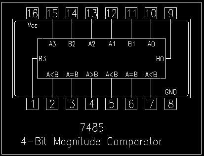
25 EXPERIMENT 4 VERIFICATION OF 4-BIT MAGNITUDE COMPARATOR Aim: - To verify the truth table of one bit and four bit comparators using logic Gates and IC 7485 Apparatus : - IC s -7486, 7404, 7408 and 7485 Circuit diagrams: 0
26 IC 7486 (4 bit Magnitude comparator) pin configuration:
27 IC 7486 (4 bit Magnitude comparator) Logic diagram:
28
29 DESCRIPTION: The 74F85 is a 4-bit magnitude comparator that can be expanded to almost any length. It compares two 4-bit binary, BCD, or other monotonic codes and presents the three possible magnitude results at the outputs. The 4-bit inputs are weighted (A0 A) and (B0 B) where A and B are the most significant bits. The operation of the74f85 is described in the Function Table, showing all possible logic conditions. The upper part of the table describes the normal operation under all conditions that will occur in a single device or in a series expansion scheme. In the upper part of the table the three outputs are mutually exclusive. In the lower part of the table, the outputs reflect the feed-forward conditions that exist in the parallel expansion scheme. The expansion inputs IA>B, and IA=B and IA<B are the least significant bit positions. When used for series expansion, the A>B, A=B and A<B outputs of the lease significant word are connected to the corresponding IA>B, IA=B and IA<B inputs of the next higher stage. Stages can be added in this manner to any length, but a propagation delay penalty of about 5ns is added with each additional stage. For proper operation, the expansion inputs of the least significant word should be tied as follows: IA>B = Low, Procedure: -. Connect the circuit as shown in fig. Feed the 4-bit binary words A0, A, A, A and B0, B, B, B from the logic input switches.. Pin of IC 7485 should be at logic to enable compare operation.. Observe the output A>B, A=B, and A<B on logic indicators. The outputs must be or 0 respectively. 4. Repeat the steps, and for various inputs A0,A, A, A and B0, B, B, B and observe the outputs at A>B, A=B and A<B. Precautions:. All the connections should be made properly.. IC should not be reversed. Result: The truth tables of one bit and four bit magnitude comparators are verified. Questions :-. What is Comparator?. What are the applications of Comparator?. Which logic is used as bit comparator? 4
30 EXPERIMENT 5 DESIGN OF DECODERS LIKE BCD-DECIMAL DECODER Aim: To design BCD-Decimal Decoder Apparatus:. IC s - 74, Electronic Circuit Designer. Connecting patch chords. Circuit Diagram:- 5
31 Truth Table: Decimal Digit Binary Inputs Logic Function Procedure:. Connections are made as per the circuit diagram. Switch on the power supply. Apply different combinations of inputs and observe the outputs; compare the outputs with the truth tables. Precautions: All the connections should be made properly. Result: BCD-Decimal decoder is designed and truth table is verified. 6
32 EXPERIMENT 6 APPLICATIONS OF IC PARALLEL ADDER ( S AND S COMPLIMENT ADDITION) Aim: Design of 4-bit IC parallel adder Apparatus : - IC s -7486, 7404, 7408 and 7485 Circuit diagrams: Description: The circuit performs addition as well as subtraction.when s input is low the circuit performs addition.the EX-OR gate acts as a controlled inverter (i.e., it inverts input when control is high, otherwise it passes the input to the output).the output of EX-OR gate is B when s input is low.the output of the circuit is sum of two input numbers when s input is low.when s input is HIGH the EX-OR gate acts as inverter and its output is the complement of input.the carry input of the first full adder is.the output of the circuit is the sum A, complement of B and.this performs s complement subtraction.the output of the circuit is in true magnitude form if the A>B.The output of the circuit is in s complement form if the A<B. 7
33 Procedure:. Connections are made as per the circuit diagram. Switch on the power supply. Apply different combinations of inputs and observe the outputs. Precautions: All the connections should be made properly. Result: 4-bit IC parallel adder is designed and s & s complement addition is performed 8
34 EXPERIMENT 7 DESIGN OF CODE CONVERTORS (BINARY TO GRAY AND GRAY TO BINARYCONVERSION) Aim: To design code converters and verify their truth tables Apparatus:. IC Electronic circuit designer.connecting patch chords Circuit Diagrams: Truth table B B B B0 Binary to Gray Code Converter G 7486 G 7486 G 7486 G0 B B B BO G G G G
35 Gray to Binary Code Converter G G G G B B B B0 G G G GO B B B B Procedure: -. The circuit connections are made as shown in fig.. Pin (4) is connected to +Vcc and Pin (7) to ground. In the case of binary to gray conversion, the inputs B0, B, B and B are given at respective pins and outputs G0, G, G, G are taken for all the 6 combinations of the input. 4. In the case of gray to binary conversion, the inputs G0, G, G and G are given at respective Pins and outputs B0, B, B, and B are taken for all the 6 combinations of inputs. 5. The values of the outputs are tabulated. Result: code converters are designed and their truth tables are verified. Precautions: All the connections should be made properly. Questions:. Convert binary 0000 to gray code. 0
36 EXPERIMENT 8 DESIGN OF MULTIPLEXERS/DEMULTIPLEXERS Aim: To design Multiplexer and Demultiplexer and verify their truth tables Apparatus:. IC ,74,74,7408. Electronic circuit designer.connecting patch chords Circuit Diagrams: MULTIPLEXER S S0 Y 0 0 I0 0 I 0 I I S S I I I I 74
37 Demultiplexer A B Y0 A B Y Y Y Y Y Y 7408 Y Procedure:. Connections are made as per the circuit diagram. Switch on the power supply. Apply different combinations of inputs and observe the outputs; compare the outputs with the truth tables. Precautions: All the connections should be made properly. Result: Multiplexer and Demultiplexer are constructed and the truth tables are verified Questions:. What is the difference between multiplexer and decoder
38 EXPERIMENT 9 VERIFICATION OF TRUTH TABLES OF FLIPFLOPS USING GATES Aim: To design and construct basic flip-flops R-S,J-K,J-K Master slave flip-flops using gates and verify their truth tables Apparatus:. IC s , 740, Electronic circuit designer. Connecting patch chords Circuit Diagrams:- Basic flipflop using NAND gates Truth Table S R Q 0 0 Forbidden No Change Basic flipflop using NOR gates S R Q 0 0 No Change Forbidden
39 R-S flip-flop using NAND gates S R Q 0 0 No Change Forbidden J-k flip-flop using NAND gates J K Q 0 0 No Change Race around 4
40 J-K Master Slave using NAND gates J K Q Procedure:. Connect the Flip-flop circuits as shown above.. Apply different combinations of inputs and observe the outputs Precautions: All the connections should be made properly. Result: Different Flip-flops using gates are constructed and their truth tables are verified Questions:.List four Basic Flip-flop applications?. What advantage does a J-K Flip-flop have over an S-R?. What is meant by Race around condition? 5
41 EXPERIMENT 0 DESIGN OF SHIFT REGISTER(TO VERIFY SERIAL TO PARALLEL,PARALLEL TO SERIAL,SERIAL TO SERIAL,PARALLEL TO PARALLEL)USING FLIP-FLOPS Aim:- To study shift register using IC 7495 in all its modes i.e. SIPO/SISO, PISO/PIPO. Apparatus: - IC 7495, etc. Circuit diagram : 6
42 PISO: 7
43 Procedure : Serial In Parallel Out(SIPO):. Connections are made as per circuit diagram.. Apply the data at serial i/p. Apply one clock pulse at clock (Right Shift) observe this data at QA. 4. Apply the next data at serial i/p. 5. Apply one clock pulse at clock, observe that the data on QA will shift to QB and the new data applied will appear at QA. 6. Repeat steps and till all the 4 bits data are entered one by one into the shift register. Serial In Serial Out (SISO):. Connections are made as per circuit diagram.. Load the shift register with 4 bits of data one by one serially.. At the end of 4th clock pulse the first data d0 appears at QD. 4. Apply another clock pulse; the second data d appears at QD. 5. Apply another clock pulse; the third data appears at QD. 6. Application of next clock pulse will enable the 4th data d to appear at QD. Thus the data applied serially at the input comes out serially at QD Parallel In Serial Out (PISO):. Connections are made as per circuit diagram.. Apply the desired 4 bit data at A, B, C and D. 8
44 . Keeping the mode control M= apply one clock pulse. The data applied at A, B, C and D will appear at QA, QB, QC and QD respectively. 4. Now mode control M=0. Apply clock pulses one by one and observe the Data coming out serially at QD Parallel In Parallel Out (PIPO):. Connections are made as per circuit diagram.. Apply the 4 bit data at A, B, C and D.. Apply one clock pulse at Clock (Note: Mode control M=). 4. The 4 bit data at A, B, C and D appears at QA, QB, QC and QD respectively. Precautions: All the connections should be made properly. Result: shift registers using IC 7495 in all its modes i.e.sipo/siso, PISO/PIPO are verified. 9
45 EXPERIMENT DESIGN OF RING AND JOHNSON COUNTERS USING FLIP-FLOPS Aim: To design Ring counter and Johnson counter and verify their truth tables Apparatus:. IC s , 740, Electronic circuit designer. Connecting patch chords Circuit Diagram: Ring Counter: Truth Table Clk Q Q Q
46 Johnson Counter: Truth Table Procedure: Clk Q Q Q Connections are made as per the circuit diagram. Switch on the power supply.. Apply clock pulses and note the outputs after each clock pulse Precautions:. All the connections should be made properly.. IC should not be reversed. Result: Ring counter and Johnson counter are designed and their truth tables are verified.
47 EXPERIMENT CONVERTION OF FLIP-FLOPS (JK-T,JK-D) Aim: To design and construct T and D Flip-flop from JK- flip-flop and verify their truth tables Apparatus: Circuit diagram:. IC s - 740, Electronic circuit designer. Connecting patch chords T-Flip Flop D-Flip Flop
48 Procedure:. Connections are made as per the circuit diagram. Switch on the power supply. Apply different combinations of inputs and observe the out puts Precautions:. All the connections should be made properly.. IC should not be reversed. Result: T and D Flip-flop are designed and constructed from JK- flip-flop and their truth tables are verified.
49 EXPERIMENT DESIGN OF BINARY/DECADE COUNTER Aim: To design and construct decade counter and verify the truth table Apparatus: Circuit diagram: Decade Counter:. IC s - 740, Electronic circuit designer. Connecting patch chords Truth Table CLK Q Q Q Q
50 Procedure:. Connections are made as per the circuit diagram. Switch on the power supply.. Apply clock pulses and note the outputs after each clock pulse and note done the out puts Q, Q, Q, Q0. Precautions:. All the connections should be made properly.. IC should not be reversed. Result: Decade counter is designed and truth tables are verified. 5
51 EXPERIMENT 4 DESIGN OFASYNCHRONOUS COUNTER, MOD COUNTER, UP COUNTER, DOWN COUNTER AND UP/DOWN COUNTER USING FLIP FLOPS Aim:- To design and construct of -bit Asynchronous up and down counters,-bit up/down counter. Apparatus: Circuit Diagram:. IC s ,7476,7400,74. Electronic circuit designer. Connecting patch chords -bit Asynchronous up counter: 6

52 -bit Asynchronous down counter: TRUTH TABLE 7

53 Two Bit up/down Counter using negative edge-triggered flipflops WHEN M= WHEN M=0 CLK Q Q 0 0 8
54 CLK Q Q Procedure:. Connections are made as per the circuit diagram. Switch on the power supply.. Apply clock pulses and note the outputs after each clock pulse and note done the out puts. Precautions:. All the connections should be made properly.. IC should not be reversed. Result: -bit Asynchronous up and down counters,-bit up/down counter are designed and truth tables are verified. 9
55 EXPERIMENT 5 DESIGN OF SYNCHRONOUS COUNTER, MOD COUNTER, UP COUNTER, DOWN COUNTER AND UP/DOWN COUNTER USING FLIP FLOPS Aim:- To design and construct of -bit Synchronous up and down counters,-bit up/down counter. Apparatus: Circuit Diagram:. IC s ,7476,7400,74. Electronic circuit designer. Connecting patch chords 40

56 Truth Table Two Bit up/down Counter using negative edge-triggered flip-flops WHEN M= WHEN M=0 CLK Q Q CLK Q Q
57 Procedure:. Connections are made as per the circuit diagram. Switch on the power supply.. Apply clock pulses and note the outputs after each clock pulse and note done the out puts. Precautions:. All the connections should be made properly.. IC should not be reversed. Result: -bit Synchronous up and down counters,-bit up/down counter are designed and truth tables are verified. 4
Dev Bhoomi Institute Of Technology Department of Electronics and Communication Engineering PRACTICAL INSTRUCTION SHEET
 Dev Bhoomi Institute Of Technology Department of Electronics and Communication Engineering PRACTICAL INSTRUCTION SHEET LABORATORY MANUAL EXPERIMENT NO. 1 ISSUE NO. : ISSUE DATE: REV. NO. : REV. DATE :
DEPARTMENT OF COMPUTER SCIENCE & ENGINEERING
 DRONACHARYA GROUP OF INSTITUTIONS, GREATER NOIDA Affiliated to Mahamaya Technical University, Noida Approved by AICTE DEPARTMENT OF COMPUTER SCIENCE & ENGINEERING Lab Manual for Computer Organization Lab
Logic Design Viva Question Bank Compiled By Channveer Patil
 Logic Design Viva Question Bank Compiled By Channveer Patil Title of the Practical: Verify the truth table of logic gates AND, OR, NOT, NAND and NOR gates/ Design Basic Gates Using NAND/NOR gates. Q.1
Module -5 Sequential Logic Design
 Module -5 Sequential Logic Design 5.1. Motivation: In digital circuit theory, sequential logic is a type of logic circuit whose output depends not only on the present value of its input signals but on
Sequential Digital Design. Laboratory Manual. Experiment #7. Counters
 The Islamic University of Gaza Engineering Faculty Department of Computer Engineering Spring 2018 ECOM 2022 Khaleel I. Shaheen Sequential Digital Design Laboratory Manual Experiment #7 Counters Objectives
Analogue Versus Digital [5 M]
![Analogue Versus Digital [5 M]](/thumbs/93/111640168.jpg "Analogue Versus Digital [5 M]") Q.1 a. Analogue Versus Digital [5 M] There are two basic ways of representing the numerical values of the various physical quantities with which we constantly deal in our day-to-day lives. One of the ways,
Q.1 a. Analogue Versus Digital [5 M] There are two basic ways of representing the numerical values of the various physical quantities with which we constantly deal in our day-to-day lives. One of the ways,
Solution to Digital Logic )What is the magnitude comparator? Design a logic circuit for 4 bit magnitude comparator and explain it,
What is the magnitude comparator? Design a logic circuit for 4 bit magnitude comparator and explain it,") Solution to Digital Logic -2067 Solution to digital logic 2067 1.)What is the magnitude comparator? Design a logic circuit for 4 bit magnitude comparator and explain it, A Magnitude comparator is a combinational
Solution to Digital Logic -2067 Solution to digital logic 2067 1.)What is the magnitude comparator? Design a logic circuit for 4 bit magnitude comparator and explain it, A Magnitude comparator is a combinational
TRAINING KITS ON DIGITAL ELECTRONIC EXPERIMENTS. Verify Truth table for TTL IC s AND, NOT, & NAND GATES
 TRAINING KITS ON DIGITAL ELECTRONIC EXPERIMENTS CEE 2800 Basic Logic Gates using TTL IC's (7 in 1) To verify the truth table For TTL AND, OR. NOT, NAND,NOR, EX-OR, & EX-NOR Gates. Instrument comprises
WINTER 15 EXAMINATION Model Answer
 Important Instructions to examiners: 1) The answers should be examined by key words and not as word-to-word as given in the model answer scheme. 2) The model answer and the answer written by candidate
PHYSICS 5620 LAB 9 Basic Digital Circuits and Flip-Flops
 PHYSICS 5620 LAB 9 Basic Digital Circuits and Flip-Flops Objective Construct a two-bit binary decoder. Study multiplexers (MUX) and demultiplexers (DEMUX). Construct an RS flip-flop from discrete gates.
MODULE 3. Combinational & Sequential logic
 MODULE 3 Combinational & Sequential logic Combinational Logic Introduction Logic circuit may be classified into two categories. Combinational logic circuits 2. Sequential logic circuits A combinational
1. Convert the decimal number to binary, octal, and hexadecimal.
 1. Convert the decimal number 435.64 to binary, octal, and hexadecimal. 2. Part A. Convert the circuit below into NAND gates. Insert or remove inverters as necessary. Part B. What is the propagation delay
RAO PAHALD SINGH GROUP OF INSTITUTIONS BALANA(MOHINDER GARH)123029
123029") DIGITAL ELECTRONICS LAB( EE-224-F) DIGITAL ELECTRONICS LAB (EE-224-F) LAB MANUAL IV SEMESTER RAO PAHALD SINGH GROUP OF INSTITUTIONS BALANA(MOHINDER GARH)2329 Department Of Electronics & Communication Engg.
DIGITAL ELECTRONICS LAB( EE-224-F) DIGITAL ELECTRONICS LAB (EE-224-F) LAB MANUAL IV SEMESTER RAO PAHALD SINGH GROUP OF INSTITUTIONS BALANA(MOHINDER GARH)2329 Department Of Electronics & Communication Engg.
NORTHWESTERN UNIVERSITY TECHNOLOGICAL INSTITUTE
 NORTHWESTERN UNIVERSITY TECHNOLOGICL INSTITUTE ECE 270 Experiment #8 DIGITL CIRCUITS Prelab 1. Draw the truth table for the S-R Flip-Flop as shown in the textbook. Draw the truth table for Figure 7. 2.
DIGITAL SYSTEM FUNDAMENTALS (ECE421) DIGITAL ELECTRONICS FUNDAMENTAL (ECE422) COUNTERS
 DIGITAL ELECTRONICS FUNDAMENTAL (ECE422) COUNTERS") COURSE / CODE DIGITAL SYSTEM FUNDAMENTALS (ECE421) DIGITAL ELECTRONICS FUNDAMENTAL (ECE422) COUNTERS One common requirement in digital circuits is counting, both forward and backward. Digital clocks and
COURSE / CODE DIGITAL SYSTEM FUNDAMENTALS (ECE421) DIGITAL ELECTRONICS FUNDAMENTAL (ECE422) COUNTERS One common requirement in digital circuits is counting, both forward and backward. Digital clocks and
Scanned by CamScanner
 NAVEEN RAJA VELCHURI DSD & Digital IC Applications Example: 2-bit asynchronous up counter: The 2-bit Asynchronous counter requires two flip-flops. Both flip-flop inputs are connected to logic 1, and initially
SEQUENTIAL LOGIC. Satish Chandra Assistant Professor Department of Physics P P N College, Kanpur
 SEQUENTIAL LOGIC Satish Chandra Assistant Professor Department of Physics P P N College, Kanpur www.satish0402.weebly.com OSCILLATORS Oscillators is an amplifier which derives its input from output. Oscillators
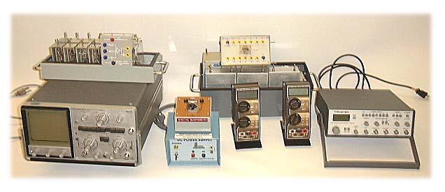
Laboratory 1 - Introduction to Digital Electronics and Lab Equipment (Logic Analyzers, Digital Oscilloscope, and FPGA-based Labkit)
") Massachusetts Institute of Technology Department of Electrical Engineering and Computer Science 6. - Introductory Digital Systems Laboratory (Spring 006) Laboratory - Introduction to Digital Electronics
Massachusetts Institute of Technology Department of Electrical Engineering and Computer Science 6. - Introductory Digital Systems Laboratory (Spring 006) Laboratory - Introduction to Digital Electronics
Bachelor Level/ First Year/ Second Semester/ Science Full Marks: 60 Computer Science and Information Technology (CSc. 151) Pass Marks: 24
 Pass Marks: 24") 2065 Computer Science and Information Technology (CSc. 151) Pass Marks: 24 Time: 3 hours. Candidates are required to give their answers in their own words as for as practicable. Attempt any TWO questions:
2065 Computer Science and Information Technology (CSc. 151) Pass Marks: 24 Time: 3 hours. Candidates are required to give their answers in their own words as for as practicable. Attempt any TWO questions:
Chapter 4. Logic Design
 Chapter 4 Logic Design 4.1 Introduction. In previous Chapter we studied gates and combinational circuits, which made by gates (AND, OR, NOT etc.). That can be represented by circuit diagram, truth table
EXPERIMENT: 1. Graphic Symbol: OR: The output of OR gate is true when one of the inputs A and B or both the inputs are true.
 EXPERIMENT: 1 DATE: VERIFICATION OF BASIC LOGIC GATES AIM: To verify the truth tables of Basic Logic Gates NOT, OR, AND, NAND, NOR, Ex-OR and Ex-NOR. APPARATUS: mention the required IC numbers, Connecting
Digital Circuits I and II Nov. 17, 1999
 Physics 623 Digital Circuits I and II Nov. 17, 1999 Digital Circuits I 1 Purpose To introduce the basic principles of digital circuitry. To understand the small signal response of various gates and circuits
AIM: To study and verify the truth table of logic gates
 EXPERIMENT: 1- LOGIC GATES AIM: To study and verify the truth table of logic gates LEARNING OBJECTIVE: Identify various Logic gates and their output. COMPONENTS REQUIRED: KL-31001 Digital Logic Lab( Main
CHAPTER 6 COUNTERS & REGISTERS
 CHAPTER 6 COUNTERS & REGISTERS 6.1 Asynchronous Counter 6.2 Synchronous Counter 6.3 State Machine 6.4 Basic Shift Register 6.5 Serial In/Serial Out Shift Register 6.6 Serial In/Parallel Out Shift Register
Laboratory 10. Required Components: Objectives. Introduction. Digital Circuits - Logic and Latching (modified from lab text by Alciatore)
") Laboratory 10 Digital Circuits - Logic and Latching (modified from lab text by Alciatore) Required Components: 1x 330 resistor 4x 1k resistor 2x 0.F capacitor 1x 2N3904 small signal transistor 1x LED 1x
Laboratory 10 Digital Circuits - Logic and Latching (modified from lab text by Alciatore) Required Components: 1x 330 resistor 4x 1k resistor 2x 0.F capacitor 1x 2N3904 small signal transistor 1x LED 1x
UNIT-3: SEQUENTIAL LOGIC CIRCUITS
 UNIT-3: SEQUENTIAL LOGIC CIRCUITS STRUCTURE 3. Objectives 3. Introduction 3.2 Sequential Logic Circuits 3.2. NAND Latch 3.2.2 RS Flip-Flop 3.2.3 D Flip-Flop 3.2.4 JK Flip-Flop 3.2.5 Edge Triggered RS Flip-Flop
TYPICAL QUESTIONS & ANSWERS
 DIGITALS ELECTRONICS TYPICAL QUESTIONS & ANSWERS OBJECTIVE TYPE QUESTIONS Each Question carries 2 marks. Choose correct or the best alternative in the following: Q.1 The NAND gate output will be low if
OFC & VLSI SIMULATION LAB MANUAL
 DEVBHOOMI INSTITUTE OF TECHNOLOGY FOR WOMEN, DEHRADUN - 24847 DEPARTMENT OF ELECTRONICS AND COMMUNICATION ENGINEERING Prepared BY: Ajay Kumar Gautam Asst. Prof. Electronics & Communication Engineering
MODEL QUESTIONS WITH ANSWERS THIRD SEMESTER B.TECH DEGREE EXAMINATION DECEMBER CS 203: Switching Theory and Logic Design. Time: 3 Hrs Marks: 100
 MODEL QUESTIONS WITH ANSWERS THIRD SEMESTER B.TECH DEGREE EXAMINATION DECEMBER 2016 CS 203: Switching Theory and Logic Design Time: 3 Hrs Marks: 100 PART A ( Answer All Questions Each carries 3 Marks )
Flip Flop. S-R Flip Flop. Sequential Circuits. Block diagram. Prepared by:- Anwar Bari
 Sequential Circuits The combinational circuit does not use any memory. Hence the previous state of input does not have any effect on the present state of the circuit. But sequential circuit has memory
Dev Bhoomi Institute Of Technology PRACTICAL INSTRUCTION SHEET EXPERIMENT NO. ISSUE NO. : ISSUE DATE: REV. NO. : REV. DATE : PAGE:
 Dev Bhoomi Institute Of Technology LABORATORY MANUAL PRACTICAL INSTRUCTION SHEET EXPERIMENT NO. ISSUE NO. : ISSUE DATE: REV. NO. : REV. DATE : PAGE: LABORATORY Name & Code: Digital Electronics SEMESTER:
1 Hour Sample Test Papers: Sample Test Paper 1. Roll No.
 6.1.2 Sample Test Papers: Sample Test Paper 1 Roll No. Institute Name: Course Code: EJ/EN/ET/EX/EV/IC/IE/IS/MU/DE/ED/ET/IU Subject: Principles of Digital Techniques Marks: 25 1 Hour 1. All questions are
Chapter 7 Counters and Registers
 Chapter 7 Counters and Registers Chapter 7 Objectives Selected areas covered in this chapter: Operation & characteristics of synchronous and asynchronous counters. Analyzing and evaluating various types
Tribhuvan University Institute of Science and Technology Bachelor of Science in Computer Science and Information Technology
 Tribhuvan University Institute of Science and Technology Bachelor of Science in Computer Science and Information Technology Course Title: Digital Logic Full Marks: 60 + 0 + 0 Course No.: CSC Pass Marks:
Chapter 2. Digital Circuits
 Chapter 2. Digital Circuits Logic gates Flip-flops FF registers IC registers Data bus Encoders/Decoders Multiplexers Troubleshooting digital circuits Most contents of this chapter were covered in 88-217
MODULAR DIGITAL ELECTRONICS TRAINING SYSTEM
 MODULAR DIGITAL ELECTRONICS TRAINING SYSTEM MDETS UCTECH's Modular Digital Electronics Training System is a modular course covering the fundamentals, concepts, theory and applications of digital electronics.
R13 SET - 1 '' ''' '' ' '''' Code No: RT21053
 SET - 1 1. a) What are the characteristics of 2 s complement numbers? b) State the purpose of reducing the switching functions to minimal form. c) Define half adder. d) What are the basic operations in
The University of Texas at Dallas Department of Computer Science CS 4141: Digital Systems Lab
 The University of Texas at Dallas Department of Computer Science CS 4141: Digital Systems Lab Experiment #5 Shift Registers, Counters, and Their Architecture 1. Introduction: In Laboratory Exercise # 4,
Sequential Digital Design. Laboratory Manual. Experiment #3. Flip Flop Storage Elements
 The Islamic University of Gaza Engineering Faculty Department of Computer Engineering Spring 2018 ECOM 2022 Khaleel I. Shaheen Sequential Digital Design Laboratory Manual Experiment #3 Flip Flop Storage
TIME SCHEDULE. MODULE TOPICS PERIODS 1 Number system & Boolean algebra 17 Test I 1 2 Logic families &Combinational logic
 COURSE TITLE : DIGITAL INSTRUMENTS PRINCIPLE COURSE CODE : 3075 COURSE CATEGORY : B PERIODS/WEEK : 4 PERIODS/SEMESTER : 72 CREDITS : 4 TIME SCHEDULE MODULE TOPICS PERIODS 1 Number system & Boolean algebra
Sequential Logic Basics
 Sequential Logic Basics Unlike Combinational Logic circuits that change state depending upon the actual signals being applied to their inputs at that time, Sequential Logic circuits have some form of inherent
Logic Design. Flip Flops, Registers and Counters
 Logic Design Flip Flops, Registers and Counters Introduction Combinational circuits: value of each output depends only on the values of inputs Sequential Circuits: values of outputs depend on inputs and
Department of Electrical Engineering University of Hail Ha il - Saudi Arabia
 Department of Electrical Engineering University of Hail Ha il - Saudi Arabia Laboratory Manual EE 200 Digital Logic Circuit Design October 2017 1 PREFACE This document is prepared to serve as a laboratory
YEDITEPE UNIVERSITY DEPARTMENT OF COMPUTER ENGINEERING. EXPERIMENT VIII: FLIP-FLOPS, COUNTERS 2014 Fall
 YEDITEPE UNIVERSITY DEPARTMENT OF COMPUTER ENGINEERING EXPERIMENT VIII: FLIP-FLOPS, COUNTERS 2014 Fall Objective: - Dealing with the operation of simple sequential devices. Learning invalid condition in
MODU LE DAY. Class-A, B, AB and C amplifiers - basic concepts, power, efficiency Basic concepts of Feedback and Oscillation. Day 1
 DAY MODU LE TOPIC QUESTIONS Day 1 Day 2 Day 3 Day 4 I Class-A, B, AB and C amplifiers - basic concepts, power, efficiency Basic concepts of Feedback and Oscillation Phase Shift Wein Bridge oscillators.
Chapter 6. Flip-Flops and Simple Flip-Flop Applications
 Chapter 6 Flip-Flops and Simple Flip-Flop Applications Basic bistable element It is a circuit having two stable conditions (states). It can be used to store binary symbols. J. C. Huang, 2004 Digital Logic
Laboratory Objectives and outcomes for Digital Design Lab
 Class: SE Department of Information Technology Subject Logic Design Sem : III Course Objectives and outcomes for LD Course Objectives: Students will try to : COB1 Understand concept of various components.
Vignana Bharathi Institute of Technology UNIT 4 DLD
 DLD UNIT IV Synchronous Sequential Circuits, Latches, Flip-flops, analysis of clocked sequential circuits, Registers, Shift registers, Ripple counters, Synchronous counters, other counters. Asynchronous
Sri Vidya College of Engineering And Technology. Virudhunagar Department of Electrical and Electronics Engineering
 Sri Vidya College of Engineering And Technology Virudhunagar 626 005 Department of Electrical and Electronics Engineering Year/ Semester/ Class : II/ III/ EEE Academic Year: 2017-2018 Subject Code/ Name:
R13. II B. Tech I Semester Regular Examinations, Jan DIGITAL LOGIC DESIGN (Com. to CSE, IT) PART-A
 PART-A") SET - 1 Note: Question Paper consists of two parts (Part-A and Part-B) Answer ALL the question in Part-A Answer any THREE Questions from Part-B a) What are the characteristics of 2 s complement numbers?
SET - 1 Note: Question Paper consists of two parts (Part-A and Part-B) Answer ALL the question in Part-A Answer any THREE Questions from Part-B a) What are the characteristics of 2 s complement numbers?
Experiment 8 Introduction to Latches and Flip-Flops and registers
 Experiment 8 Introduction to Latches and Flip-Flops and registers Introduction: The logic circuits that have been used until now were combinational logic circuits since the output of the device depends
MAHARASHTRA STATE BOARD OF TECHNICAL EDUCATION (Autonomous) (ISO/IEC Certified)
 (ISO/IEC Certified)") Important Instructions to examiners: 1) The answers should be examined by key words and not as word-to-word as given in the model answer scheme. 2) The model answer and the answer written by candidate
Important Instructions to examiners: 1) The answers should be examined by key words and not as word-to-word as given in the model answer scheme. 2) The model answer and the answer written by candidate
Counter dan Register
 Counter dan Register Introduction Circuits for counting events are frequently used in computers and other digital systems. Since a counter circuit must remember its past states, it has to possess memory.
Physics 323. Experiment # 10 - Digital Circuits
 Physics 323 Experiment # 10 - Digital Circuits Purpose This is a brief introduction to digital (logic) circuits using both combinational and sequential logic. The basic building blocks will be the Transistor
MUHAMMAD NAEEM LATIF MCS 3 RD SEMESTER KHANEWAL
 1. A stage in a shift register consists of (a) a latch (b) a flip-flop (c) a byte of storage (d) from bits of storage 2. To serially shift a byte of data into a shift register, there must be (a) one click
ME 515 Mechatronics. Introduction to Digital Electronics
 ME 55 Mechatronics /5/26 ME 55 Mechatronics Digital Electronics Asanga Ratnaweera Department of Faculty of Engineering University of Peradeniya Tel: 8239 (3627) Email: asangar@pdn.ac.lk Introduction to
QUICK GUIDE COMPUTER LOGICAL ORGANIZATION - OVERVIEW
 QUICK GUIDE http://www.tutorialspoint.com/computer_logical_organization/computer_logical_organization_quick_guide.htm COMPUTER LOGICAL ORGANIZATION - OVERVIEW Copyright tutorialspoint.com In the modern
Experiment (6) 2- to 4 Decoder. Figure 8.1 Block Diagram of 2-to-4 Decoder 0 X X
 2- to 4 Decoder. Figure 8.1 Block Diagram of 2-to-4 Decoder 0 X X") 8. Objectives : Experiment (6) Decoders / Encoders To study the basic operation and design of both decoder and encoder circuits. To describe the concept of active low and active-high logic signals. To
8. Objectives : Experiment (6) Decoders / Encoders To study the basic operation and design of both decoder and encoder circuits. To describe the concept of active low and active-high logic signals. To
Final Exam review: chapter 4 and 5. Supplement 3 and 4
 Final Exam review: chapter 4 and 5. Supplement 3 and 4 1. A new type of synchronous flip-flop has the following characteristic table. Find the corresponding excitation table with don t cares used as much
North Shore Community College
 North Shore Community College Course Number: IEL217 Section: MAL Course Name: Digital Electronics 1 Semester: Credit: 4 Hours: Three hours of Lecture, Two hours Laboratory per week Thursdays 8:00am (See
MAHARASHTRA STATE BOARD OF TECHNICAL EDUCATION (Autonomous) (ISO/IEC Certified) WINTER 2018 EXAMINATION MODEL ANSWER
 (ISO/IEC Certified) WINTER 2018 EXAMINATION MODEL ANSWER") Important Instructions to examiners: 1) The answers should be examined by key words and not as word-to-word as given in themodel answer scheme. 2) The model answer and the answer written by candidate may
Important Instructions to examiners: 1) The answers should be examined by key words and not as word-to-word as given in themodel answer scheme. 2) The model answer and the answer written by candidate may
Find the equivalent decimal value for the given value Other number system to decimal ( Sample)
") VELAMMAL COLLEGE OF ENGINEERING AND TECHNOLOGY, MADURAI 65 009 Department of Information Technology Model Exam-II-Question bank PART A (Answer for all Questions) (8 X = 6) K CO Marks Find the equivalent
VELAMMAL COLLEGE OF ENGINEERING AND TECHNOLOGY, MADURAI 65 009 Department of Information Technology Model Exam-II-Question bank PART A (Answer for all Questions) (8 X = 6) K CO Marks Find the equivalent
IT T35 Digital system desigm y - ii /s - iii
 UNIT - III Sequential Logic I Sequential circuits: latches flip flops analysis of clocked sequential circuits state reduction and assignments Registers and Counters: Registers shift registers ripple counters
RS flip-flop using NOR gate
 RS flip-flop using NOR gate Triggering and triggering methods Triggering : Applying train of pulses, to set or reset the memory cell is known as Triggering. Triggering methods:- There are basically two
EXPERIMENT #6 DIGITAL BASICS
 EXPERIMENT #6 DIGITL SICS Digital electronics is based on the binary number system. Instead of having signals which can vary continuously as in analog circuits, digital signals are characterized by only
DIGITAL SYSTEM DESIGN UNIT I (2 MARKS)
") DIGITAL SYSTEM DESIGN UNIT I (2 MARKS) 1. Convert Binary number (111101100) 2 to Octal equivalent. 2. Convert Binary (1101100010011011) 2 to Hexadecimal equivalent. 3. Simplify the following Boolean function
DIGITAL SYSTEM DESIGN UNIT I (2 MARKS) 1. Convert Binary number (111101100) 2 to Octal equivalent. 2. Convert Binary (1101100010011011) 2 to Hexadecimal equivalent. 3. Simplify the following Boolean function
DepartmentofElectronicEngineering NEDUniversity ofengineering &Technology LABORATORY WORKBOOK DIGITAL LOGIC DESIGN (TC-201)
") DepartmentofElectronicEngineering NEDUniversity ofengineering &Technology LABORATORY WORKBOOK DIGITAL LOGIC DESIGN (TC-201) Instructor Name: Student Name: Roll Number: Semester: Batch: Year: Department:
DepartmentofElectronicEngineering NEDUniversity ofengineering &Technology LABORATORY WORKBOOK DIGITAL LOGIC DESIGN (TC-201) Instructor Name: Student Name: Roll Number: Semester: Batch: Year: Department:
MC9211 Computer Organization
 MC9211 Computer Organization Unit 2 : Combinational and Sequential Circuits Lesson2 : Sequential Circuits (KSB) (MCA) (2009-12/ODD) (2009-10/1 A&B) Coverage Lesson2 Outlines the formal procedures for the
Jawaharlal Nehru Engineering College
 Jawaharlal Nehru Engineering College Laboratory Manual DIGITAL LOGIC DESIGN For Second Year Students Manual made by Dr. V. A. More Author JNEC, Aurangabad MGM S Jawaharlal Nehru Engineering College N-6,
Registers and Counters
 Registers and Counters Clocked sequential circuit = F/Fs and combinational gates Register Group of flip-flops (share a common clock and capable of storing one bit of information) Consist of a group of
MAHARASHTRA STATE BOARD OF TECHNICAL EDUCATION (Autonomous)
") Subject Code: 17320 Model Answer Page 1 of 32 Important Instructions to examiners: 1) The answers should be examined by key words and not as word-to-word as given in the Model answer scheme. 2) The model
Subject Code: 17320 Model Answer Page 1 of 32 Important Instructions to examiners: 1) The answers should be examined by key words and not as word-to-word as given in the Model answer scheme. 2) The model
Assignment 2b. ASSIGNMENT 2b. due at the start of class, Wednesday Sept 25.
 ASSIGNMENT 2b due at the start of class, Wednesday Sept 25. For each section of the assignment, the work that you are supposed to turn in is indicated in italics at the end of each problem or sub-problem.
RS flip-flop using NOR gate
 RS flip-flop using NOR gate Triggering and triggering methods Triggering : Applying train of pulses, to set or reset the memory cell is known as Triggering. Triggering methods:- There are basically two
UNIVERSITI TEKNOLOGI MALAYSIA
 SULIT Faculty of Computing UNIVERSITI TEKNOLOGI MALAYSIA FINAL EXAMINATION SEMESTER I, 2016 / 2017 SUBJECT CODE : SUBJECT NAME : SECTION : TIME : DATE/DAY : VENUES : INSTRUCTIONS : Answer all questions
NH 67, Karur Trichy Highways, Puliyur C.F, Karur District UNIT-III SEQUENTIAL CIRCUITS
 NH 67, Karur Trichy Highways, Puliyur C.F, 639 114 Karur District DEPARTMENT OF ELETRONICS AND COMMUNICATION ENGINEERING COURSE NOTES SUBJECT: DIGITAL ELECTRONICS CLASS: II YEAR ECE SUBJECT CODE: EC2203
Department of CSIT. Class: B.SC Semester: II Year: 2013 Paper Title: Introduction to logics of Computer Max Marks: 30
 Department of CSIT Class: B.SC Semester: II Year: 2013 Paper Title: Introduction to logics of Computer Max Marks: 30 Section A: (All 10 questions compulsory) 10X1=10 Very Short Answer Questions: Write
EKT 121/4 ELEKTRONIK DIGIT 1
 EKT 2/4 ELEKTRONIK DIGIT Kolej Universiti Kejuruteraan Utara Malaysia Sequential Logic Circuits - COUNTERS - LATCHES (review) S-R R Latch S-R R Latch Active-LOW input INPUTS OUTPUTS S R Q Q COMMENTS Q
Digital Systems Laboratory 3 Counters & Registers Time 4 hours
 Digital Systems Laboratory 3 Counters & Registers Time 4 hours Aim: To investigate the counters and registers constructed from flip-flops. Introduction: In the previous module, you have learnt D, S-R,
DALHOUSIE UNIVERSITY Department of Electrical & Computer Engineering Digital Circuits - ECED 220. Experiment 4 - Latches and Flip-Flops
 DLHOUSIE UNIVERSITY Department of Electrical & Computer Engineering Digital Circuits - ECED 0 Experiment - Latches and Flip-Flops Objectives:. To implement an RS latch memory element. To implement a JK
SEMESTER ONE EXAMINATIONS 2002
 SEMESTER ONE EXAMINATIONS 2002 EE101 Digital Electronics Solutions Question 1. An assembly line has 3 failsafe sensors and 1 emergency shutdown switch. The Line should keep moving unless any of the following
EE 367 Lab Part 1: Sequential Logic
 EE367: Introduction to Microprocessors Section 1.0 EE 367 Lab Part 1: Sequential Logic Contents 1 Preface 1 1.1 Things you need to do before arriving in the Laboratory............... 2 1.2 Summary of material
WINTER 14 EXAMINATION
 Subject Code: 17320 WINTER 14 EXAMINATION Model Answer Important Instructions to examiners: 1) The answers should be examined by key words and not as word-to-word as given in the model answer scheme. 2)
NEW MEXICO STATE UNIVERSITY Electrical and Computer Engineering Department. EE162 Digital Circuit Design Fall Lab 5: Latches & Flip-Flops
 NEW MEXICO STATE UNIVERSITY Electrical and Computer Engineering Department EE162 Digital Circuit Design Fall 2012 OBJECTIVES: Lab 5: Latches & Flip-Flops The objective of this lab is to examine and understand
Lecture 12. Amirali Baniasadi
 CENG 24 Digital Design Lecture 2 Amirali Baniasadi amirali@ece.uvic.ca This Lecture Chapter 6: Registers and Counters 2 Registers Sequential circuits are classified based in their function, e.g., registers.
Combinational Logic Design
 Lab #2 Combinational Logic Design Objective: To introduce the design of some fundamental combinational logic building blocks. Preparation: Read the following experiment and complete the circuits where
CHAPTER 4: Logic Circuits
 CHAPTER 4: Logic Circuits II. Sequential Circuits Combinational circuits o The outputs depend only on the current input values o It uses only logic gates, decoders, multiplexers, ALUs Sequential circuits
UNIT IV. Sequential circuit
 UNIT IV Sequential circuit Introduction In the previous session, we said that the output of a combinational circuit depends solely upon the input. The implication is that combinational circuits have no
St. MARTIN S ENGINEERING COLLEGE
 St. MARTIN S ENGINEERING COLLEGE Dhulapally, Kompally, Secunderabad-500014. Branch Year&Sem Subject Name : Electronics and Communication Engineering : II B. Tech I Semester : SWITCHING THEORY AND LOGIC
Principles of Computer Architecture. Appendix A: Digital Logic
 A-1 Appendix A - Digital Logic Principles of Computer Architecture Miles Murdocca and Vincent Heuring Appendix A: Digital Logic A-2 Appendix A - Digital Logic Chapter Contents A.1 Introduction A.2 Combinational
Engineering College. Electrical Engineering Department. Digital Electronics Lab
 Engineering College Electrical Engineering Department Digital Electronics Lab Prepared by: Dr. Samer Mayaleh Eng. Nuha Odeh 2009/2010-1 - CONTENTS Experiment Name Page 1- Measurement of Basic Logic Gates
CPS311 Lecture: Sequential Circuits
 CPS311 Lecture: Sequential Circuits Last revised August 4, 2015 Objectives: 1. To introduce asynchronous and synchronous flip-flops (latches and pulsetriggered, plus asynchronous preset/clear) 2. To introduce
Chapter 5 Sequential Circuits
 Logic and Computer Design Fundamentals Chapter 5 Sequential Circuits Part 2 Sequential Circuit Design Charles Kime & Thomas Kaminski 28 Pearson Education, Inc. (Hyperlinks are active in View Show mode)
Flip-Flops and Sequential Circuit Design
 Flip-Flops and Sequential Circuit Design ECE 52 Summer 29 Reading ssignment Brown and Vranesic 7 Flip-Flops, Registers, Counters and a Simple Processor 7.5 T Flip-Flop 7.5. Configurable Flip-Flops 7.6
VU Mobile Powered by S NO Group
 Question No: 1 ( Marks: 1 ) - Please choose one A 8-bit serial in / parallel out shift register contains the value 8, clock signal(s) will be required to shift the value completely out of the register.
Asynchronous (Ripple) Counters
 Counters") Circuits for counting events are frequently used in computers and other digital systems. Since a counter circuit must remember its past states, it has to possess memory. The chapter about flip-flops introduced
Circuits for counting events are frequently used in computers and other digital systems. Since a counter circuit must remember its past states, it has to possess memory. The chapter about flip-flops introduced
Subject : EE6301 DIGITAL LOGIC CIRCUITS
 QUESTION BANK Programme : BE Subject : Semester / Branch : III/EEE UNIT 1 NUMBER SYSTEMS AND DIGITAL LOGIC FAMILIES Review of number systems, binary codes, error detection and correction codes (Parity
Quiz #4 Thursday, April 25, 2002, 5:30-6:45 PM
 Last (family) name: First (given) name: Student I.D. #: Circle section: Hu Saluja Department of Electrical and Computer Engineering University of Wisconsin - Madison ECE/CS 352 Digital System Fundamentals
 UNIT 1 NUMBER SYSTEMS AND DIGITAL LOGIC FAMILIES 1. Briefly explain the stream lined method of converting binary to decimal number with example. 2. Give the Gray code for the binary number (111) 2. 3.
Operating Manual Ver.1.1
 Johnson Counter Operating Manual Ver.1.1 An ISO 9001 : 2000 company 94-101, Electronic Complex Pardesipura, Indore- 452010, India Tel : 91-731- 2570301/02, 4211100 Fax: 91-731- 2555643 e mail : info@scientech.bz
Laboratory 11. Required Components: Objectives. Introduction. Digital Displays and Logic (modified from lab text by Alciatore)
") Laboratory 11 Digital Displays and Logic (modified from lab text by Alciatore) Required Components: 2x lk resistors 1x 10M resistor 3x 0.1 F capacitor 1x 555 timer 1x 7490 decade counter 1x 7447 BCD to
Laboratory 11 Digital Displays and Logic (modified from lab text by Alciatore) Required Components: 2x lk resistors 1x 10M resistor 3x 0.1 F capacitor 1x 555 timer 1x 7490 decade counter 1x 7447 BCD to