Department of Electrical Engineering University of Hail Ha il - Saudi Arabia
|
|
|
- Erik Russell
- 5 years ago
- Views:
Transcription

1 Department of Electrical Engineering University of Hail Ha il - Saudi Arabia Laboratory Manual EE 200 Digital Logic Circuit Design October
2 PREFACE This document is prepared to serve as a laboratory manual for EE 200 Digital Logic Circuit Design course for electrical engineering students. The manual consists of a set of experiments which are designed to allow students to understand, develop and verify digital circuits and systems practices. This set of experiments cover relevant topics prescribed in the syllabus and are designed to reinforce the theoretical concepts taught in the classroom with practical experience in the lab. By the end of the course, students are expected to have a good understanding of digital logic design and implementation with SSI and MSI devices. 2
3 LIST OF EXPERIMENTS EE-200 DIGITAL LOGIC DESIGN INTRODUCTION LAB GUIDELINES PRE-LAB Each student will do his own pre-lab. It is intended in this course to increase the student s utilization of PC; therefore, the pre-lab write up must be typed. This same write up should be modified to be submitted as the Lab report. Starting from Lab 3, all pre-lab must be done using Logic Works simulation package. During the Lab, each student may be asked about the simulation results. All circuit parts with pin numbers should be included in the pre-lab so that you will be ready to start connecting the hardware in the lab. Try to investigate all possible changes on the circuit to acquire full knowledge about your design. All questions in the Lab handout should be answered based on the Logic Works results. The pre-lab will make 35% of the total grade of the Lab experiment. THE LAB During the lab, the students will work in groups. The Pre-Lab results from each student in the group will be compared and the circuit producing the best results will be implemented using hardware parts. Elaborate on your conclusion about the observations simulation and results obtained. Punctuality of attendance to the Lab is mandatory; the active participation in the experiments will count as 30% of the total grade. Equal marks are allocated to report and final Lab Examination. Delayed reports fetch lower marks as compared to the reports submitted on time. Each experimental report must be submitted before the following week. THE LAB REPORT Each group should submit his own report. The lab reports are intended to serve two equally important purposes. First, they indicate your technical comprehension of the topics addressed in the labs, and second, they indicate your ability to present and discuss your results in a clear and concise manner. You will be graded on both aspects of your report. The suggested format for your lab report is given below. 1. Objectives: State clearly what you set out to achieve in this lab. If this differs from what you finally achieved, explain it in the "Conclusions" section. Please do not copy the objectives verbatim from the lab handout. Think about it, interpret it, and explain it the best you can, in your own words. 2. Parts: List all parts which you used in the design. 3. Design and Test Procedure: For each subsection of the lab, explain the following: (a) Step-by-step description of what you did. Include as many details as possible, and once again, write it in your own words. (b) All necessary calculations as well as all pin-to-pin circuit diagrams of your design. Please make sure your figures are consistent, legible and well labeled. (c) Your testing procedure. Explain how you went about testing your design. Did you try testing critical individual blocks first? 4. Results and Answers to Questions: For each subsection of the lab, present your results in a clear and concise manner (label graph axes, include all units of measurement). Note down all your observations, even if you were not specifically asked for them in the handout. Interpret your results and discuss the accuracy of your measurements. Additionally, answer all questions listed in the lab handout. 5. Conclusions: In this section you should attempt to answer the questions: What did you learn from this lab? What did you do wrong (or what went wrong)? How could you have improved upon your design and test procedures? Were your results as expected or did you find something unusual. Try not to include information that you have included in previous sections. Present 3
4 significance of your results conceptually, if applicable, (e.g. The CAD tool does not capture the glitching behavior accurately.) The Lab Report will count as 50% of the grade and is due at the beginning of the subsequent lab experiment. 4
5 LABORATORY REGULATIONS AND SAFETY RULES The following Regulations and Safety Rules must be observed in all concerned laboratory location. 1. It is the duty of all concerned who use any electrical laboratory to take all reasonable steps to safeguard the HEALTH and SAFETY of themselves and all other users and visitors. 2. Be sure that all equipment is properly working before using them for laboratory exercises. Any defective equipment must be reported immediately to the Lab. Instructors or Lab. Technical Staff. 3. Students are allowed to use only the equipment provided in the experiment manual or equipment used for senior project laboratory. 4. Power supply terminals connected to any circuit are only energized with the presence of the Instructor or Lab. Staff. 5. Students should keep a safe distance from the circuit breakers, electric circuits or any moving parts during the experiment. 6. Avoid any part of your body to be connected to the energized circuit and ground. 7. Switch off the equipment and disconnect the power supplies from the circuit before leaving the laboratory. 8. Observe cleanliness and proper laboratory house keeping of the equipment and other related accessories. 9. Wear proper clothes and safety gloves or goggles required in working areas that involves fabrications of printed circuit boards, chemicals process control system, antenna communication equipment and laser facility laboratories. 10. Double check your circuit connections specifically in handling electrical power machines, AC motors and generators before switching ON the power supply. 11. Make sure that the last connection to be made in your circuit is the power supply and first thing to be disconnected is also the power supply. 12. Equipment should not be removed, transferred to any location without permission from the laboratory staff. 13. Software installation in any computer laboratory is not allowed without the permission from the Laboratory Staff. 14. Computer games are strictly prohibited in the computer laboratory. 15. Students are not allowed to use any equipment without proper orientation and actual hands on equipment operation. 16. Smoking and drinking in the laboratory are not permitted. All these rules and regulations are necessary precaution in Electrical Laboratory to safeguard the students, laboratory staff, the equipment and other laboratory users. 5
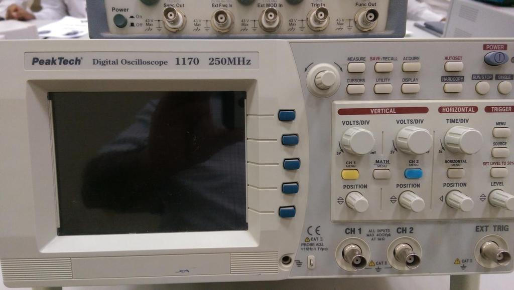
6 EE 200 DIGITAL LOGIC DESIGN EXPERIMENT #1 INTRODUCTION TO LAB EQUIPMENT OBJECTIVE To get acquaint with the breadboard, function generators and the oscilloscope etc. APPARATUS - Dual trace oscilloscope - Digital Proto-Board -Function generators THEORY See sections 1-2, and 1-6 in the book. PB-503-C Analog/Digital Proto-Board: The PB-503-C Analog/Digital Proto-Board is a self-contained digital logic laboratory. It includes a +5 volt power supply that provides operation power to the circuits under test, and also serves a 1 logic level for TTL (transistor-transistor logic) integrated circuits. The 0 logic level is represented by connection ground. Located on the front panel (see Fig 1) is a Breadboarding Socket that contains over 2500 tie points. These tie points are divided into 384 sets of five electrically interconnected solderless tie points, 8 sets of 25 interconnected solderless tie points along the right and left edges, and 4 sets of 50 interconnected solderless tie points on the top of the board. Tie points are spaced 0.1 inch apart and will accommodate the pins of DIP {dual-inline package) integrated circuits, as well as a wide variety of other circuit components. The four groups of tie points (50 tie points each) at the top of the breadboarding are connected to +5V, an adjustable (+5, 15V), an adjustable (-5, -15V), and a ground connection, respectively. In the EE200 Lab experiments, we will only use the +5V row and the ground row of tie points. The eight larger groups of tie points (25 tie points each) are handy where large number of connections are to be made to a common circuit point, e.g., extending the ground, +5volt, etc. Other useful features of the PB-503 include - Function Generator: The multi-waveform function generator provides continuously variable frequency signals from 0.1Hz to 100KHz. The frequency is selected in three ranges, with each range covering two-decades. The generator produces, sine, triangle, and square waveforms. - Logic Indicators: A bank of eight LEDs is provided for use as built-in logic indicators. The LEDs are active high (they light) to indicate a logic one condition. - Debounced Pushbuttons (Pulsers): two manual, bounceless (digitally conditioned) pulser buttons PB1 and PB2. 6

7 - Switches: An eight-pole DIP switch provides a convenient source of digital outputs. All eight switches have one side connected to a common lead, which may be switched to either +5 volts or ground. The remaining sides of all eight switches are separate, available, and uncommitted. This arrangement makes connecting special digital circuitry such as an eight-bit input port quick and easy. In addition to the eight-pole switch, there are two single pole, double throw (SPDT) switches provided for general switching functions. - Potentiometers: Two potentiometers are provided on the PB-503. The resistance values chosen (1 K and 10 K ohms) may be used in common circuit applications. - BNC Connectors: The PB-503 may be connected to other pieces of equipment via two BNC connectors BNC J1 and BNC J2. These allow the use of shielded cable to minimize noise and interference. Fig.1 PB-503 Panel layout. 7
8 IC PIN CONNECTIONs: The IC type 7493 is in a 14-pin dual in-line case. The base pins progress in a counterclockwise direction as seen from the side away from the pins, as shown Fig 2. Pin 1 is located by an identifying symbol, or the location of pins 1 and 14 are identified by an index notch at the end of the case where pins 1 and 14 are located. PROCEDURE: THE IDL Connect the PB-503 line cord into the AC power supply and turn on the power switch. 2. Connect the LOGIC INDICATORS (lamp monitor) (1, 2,,8) to +5 volts. The lamps monitors should light when connected +5 volts and this ON lamp condition will represent a l logic level in your experiments. 3. Now connect the lamp monitors to ground. They should all be off at this time. This OFF : lamp condition will represent a 0 logic level in your experiments. 4. Connect one side of a resistor (20 ohms, to 100 K) to ground and the other side to DIP switch S1-1 and switch the 5 V/GND switch to 5 volts position (These steps are already done for you). Connect S1-1 to LED-1. Now, when the S1-1 is pushed up to the closed position LED-1 will light, and when the S1-1 is brought back to the open position the LED will be off. Repeat these steps for S1-2 through S1-8 and observe the resultant condition of the lamp monitors. Switch position lamp logic level 8
 to +5 volts and the other side to PB1-1, the NC point. Then connect PB1-1 (the other lead of NC point) to LED-1.")
9 The switches can, thus, be used to supply logic level inputs to experimental circuits. 5. PULSER BUTTONS. Connect one side of a resistor (20 ohms, to 100 K) to +5 volts and the other side to PB1-1, the NC point. Then connect PB1-1 (the other lead of NC point) to LED-1. The LED should light when PB1 is pressed and extinguish when PB1 is released. Next, move the connections from PB1-1 to PB1-2, the NO point. Now the LED should be lit when PB1 is not pressed and go off when PB1 is pressed. Repeat these steps for PB2. These buttons will be used to enter momentary pulses of O and 1 logic levels. 6. Single Pole, Double Throw (SPDT) switches. Connect one side of a resistor (20 ohms, to 100 K) to +5 volts and the other side to lead 1 of S2. Then connect lead 2 to LED-1 and Lead 3 to LED-2. When the switch is brought to the up position then LED-1 and LED-2 will be ON and when the switch is brought down, the two LED s will be off. Repeat these steps on S3. These switches are provided for general switching functions. 7. CLOCK output. Connect the FUNCTION GENERATOR output TTL to LED- 1. Set the function generator to times 1 position and move the frequency control all the way to the top. Set the frequency selector to Hz. LED-1 should flash on and off, alternately at about 1 cycle per second. Move the function generator to times 10 position (setting the frequency to 10 Hz). The lamp monitors should flash on and off at a faster rate, too high to count. Higher frequency settings times 100 should cause the lamps to appear to be on continuously, at about half-normal brilliance. 8. Connect the FUNCTION GENERATOR output TTL to an oscilloscope. You should observe a square wave having fairly steep sides and a peak-to-peak. 9. Amplitude of 4 to 5 volts. Change the selection to Square, triangle, Sine and observe the waves on the oscilloscope. 9
10 10
11 EE 200 DIGITAL LOGIC DESIGN EXPERIMENT #2 DIGITAL LOGIC GATES OBJECTIVES To study the basic logic gates: AND, OR, INVERT, NAND, and NOR. To study the representation of these functions by truth tables, logic diagrams and Boolean algebra. To observe the pulse response of logic gates. To measure the propagation delay of logic gates. APPARATUS IC Type 7400 Quadruple 2-input NAND gates IC Type 7402 Quadruple 2-input NOR gates IC Type 7404 Hex Inverters IC Type 7408 Quadruple 2-input AND gates IC Type 7432 Quadruple 2-input OR gates IC Type 7486 Quadruple 2-input XOR gate Digi-Designer Logic Board Dual-trace oscilloscope THEORY AND A multi-input circuit in which the output is 1 only if all inputs are 1.The symbolic representation of the AND gate is shown in Fig. 1a. Figure 1a. OR A multi-input circuit in which the output is 1 when any input is 1. The symbolic representation of the OR gate is shown in Fig. 1b. 11
12 Figure 1b. INVERTOR The output is 0 when the input is 1, and the output is 1 when the input is 0. The symbolic representation of an inverter is shown in Fig. 1c. Figure 1c NAND AND followed by INVERT. The symbolic representation of the NAND gate is shown in Fig 1d. Figure 1d. NOR OR followed by INVERT as shown in Fig 1e. 12

13 EX-OR The output of the Exclusive OR gate, is 0 when it s two inputs are the same and it s output is 1 when its two inputs are different. Truth Table Representation of the output logic levels of a logic circuit for every possible combination of levels of the inputs. This is best done by means of a systematic tabulation. a. Two input AND gate b. Two input OR gate c. Inverter d. Two input NAND gate e. Two input NOR gate f. Two input XOR gate Part 1: Logic Functions 1. AND, OR, NAND, and NOR gates and XOR gates. Look on the data sheets for each gate, connect the circuit on Breadboard and test the gates to fill up the truth tables for each. 2. Using logic switches S1-1 and S-2, apply the logic levels 0 and 1 to gate inputs, in the sequence shown in table 1. Record the output logic levels (see lamp LED-1) in table 1. Repeat the recordings for each gate mentioned above. Remember: Lamp ON = Logic 1, (High) Lamp OFF = Logic 0 (Low) Truth Table 1. A B Y Use an inverter gate from IC, use data sheet and complete the table below. A 0 1 Y 13
14 Part-2: Response of Logic Gates: Connect the circuits of figures 2 and 3 and develop the corresponding truth tables Figure 2. Figure 3 Part 3: Review Questions: 1. Write a truth table for each circuit. Derive Boolean expressions for all outputs. 2. Calculate propagation delay for circuits 4a and confirm delay for circuit 4b. Figure 4a. 14

15 Figure 4b. 2. A burglar alarm for a car has a normally low switch on each of four doors. If any door is opened the output of that switch goes HIGH. The alarm is set off with an active-low output signal. What type of gate will provide this logic? Support your answer with an explanation 15
16 16
17 17
18 18
19 19
20 20
21 21
22 22
23 23
24 24
25 25
26 26
27 27
28 28
29 29
30 30
31 31
32 32
33 33
34 EE 200 DIGITAL LOGIC CIRCUIT DESIGN EXPERIMENT #3 BINARY AND DECIMAL NUMBERS OBJECTIVE To demonstrate the count sequence of binary number and the binary-codeddecimal (BCD) representation. APPARATUS IC type bit ripple counter BINARY COUNT 1. Turn off the power switch. 2. Connect the IC type 7493 as shown in Fig. 3 Pin 14 is connected to push button (PB1). 3. Turn the power on and observe the four indicator lamps. The 4-bit number in theout is incremented by one for every pulse generated by pushing the pulsar buttonpb1. 4. Disconnect the input of the counter at pin 14 from PB1 and connect it to the FUNCTION GENERATOR (lead TTL). 5. Set frequency selector to time 1 (1 Hz). This will provide an automatic binarycount. THE BCD COUNT 1. Turn off the power switch. 2. Connect the IC type 7493 as shown in Fig.4 Pin 14 is connected to PB1. 3. Turn the power on and observe the four indicator lamps. The 4-bit number inthe lambs is incremented by one for every pulse generated by pushing thepulser button PB1 following the sequence 0, 1, 2, 3, 4, 5, 6, 7, 8, 9, 1, 2, 3,. 4. Disconnect the input of the counter at pin 14 from PB1 and connect it to TTL.Set frequency selector to time 1 (1 Hz). This will provide an automatic binarycount 34
35 35
36 36
37 37
38 38
39 39
40 40
41 EE 200 DIGITAL LOGIC CIRCUIT DESIGN EXPERIMENT #4 BOOLEAN ALGEBRA OBJECTIVES To verify the rules and properties of Boolean Algebra To simplify and modify Boolean logic functions by means of Demorgan s Theorem. To design and implement a logic circuit using Boolean Algebra. APPARATUS PB-50/IDL Quadruple 2 input NAND gates Quadruple 2 input NOR gates 7408 Quadruple 2 input AND gates 7432 Quadruple 2 input OR gates 7404 Hex inverters 7411 Triple 3-input AND gate THEORY (See chapter 2 of the textbook) 1. A+0 = A 2. A+1 = 1 3. A.0 = 0 4. A.1 = A 5. A+A = A 6. A+A = 1 7. A.A = A 8. A.A = 0 9. (A ) = A 10. A+AB = A 11. A+A B = A+B 12. (A+B)(A+C) = A+BC 13. A. B = (A+B) 14. A +B = (A.B) Procedure 1: a. Prove rule 1 using LogicWorks. Follow the procedure given below I. Open a new design window II. III. IV. Choose ALL LIBRARY in the Parts Palette Put OR in the Filter window Select and double click on OR-2 V. Move the cursor back into the circuit window. The cursor on the screen will be replaced by a moving image of an OR gate. 41
42 VI. Position the OR gate near the center of the circuit window and click the mouse button. VII. Press the spacebar to return to point mode. VIII. Move again to the Parts Palette and type on the Filter switch or part of the word switch e.g. sw. IX. Select Binary switch and connect it to an input of the OR gate in the design window. (If you want to move the binary switch around, press the shift key while moving it). X. Move again to the Parts Palette and select ground to be connected to the other input of the OR gate. XI. Using the same method get a Binary Probe and connect it to the output of the OR gate. XII. Click on the binary switch to change it between 0 and 1 and notice how the rule A+0 = A is satisfied. In the lab connect the circuit as shown in the figure using the switch S1-1 and LED-1 to verify the rule. Fig.1 Verifying Rule 1 b. Connect the circuit of Fig.2 Using LogicWorks. Which rule does this circuit illustrate? Fig.2 In the lab connect the circuit as shown in the figure using switch S1-1 and LED-1 to verify the rule. 42
43 c. Design a circuit that illustrates rule 10. Use clock generator of PB-503 for A and one of the logic switches of S1 for B. Copy the circuit from LogicWorks and paste it in your lab report. d. Rule 6 illustrates that A+A could be replaced with a wire to Vcc. What does rule 8 illustrate? e. Rule 11 states that A+A B = A+B. Using LogicWorks design a circuit that illustrates each of these expressions. A+A B A+B Prove that these two circuits perform equivalent logic. (Connect two circuits and show that their output are same). Procedure 2: Demorgan s Theorem Proof of equation (1) Using LogicWorks construct the two circuits given in Figs.3 and 4 corresponding to the functions A. B and (A+B) respectively. Show that for all combinations of A and B, the two circuits give identical results. 1 0 A 1 2 A' B B' 9 A+B 12 A'.B' Fig A B 3 3 (A+B)' Fig.4 Proof of equation (2) Using LogicWorks construct two circuits given in Figs. 5 and 6, corresponding to the 43
44 functions A +B and (A.B) A.B, respectively. Show that, for all combinations of A and B, the two circuits give identical results. In the lab connect these circuits and verify their operations. 1 0 A 1 2 A' B B' 2 A'+B' Fig A 1 (AB)' B 2 3 Fig. 6 II. Design of a Digital Circuit Consider the following problem:- Four chairs A, B, C, and D are placed in a row. Each chair may be occupied ( l ) or empty ( 0 ). A Boolean function F is l if and only if there are two or more adjacent chairs that are empty. 1. Develop the truth table defining Boolean function F. 2. Express F as a minterm expansion (Standard Sum of Product) 3. Express F as a MAXTERM expansion (Standard Product of Sum) 4. Using postulates and theorems of Boolean algebra, simplify the minterm expansion of F to a form with as few occurrences of each as possible. 5. Implement on LogicWorks for the pre-lab and then on PB-503/IDL 800, the simplified Boolean function with logic gates and check the operation of the circuit. Notes: In LogicWorks use Binary Switches to represent the four chairs and connect the output of the circuit to a Binary Probe. Check that the Probe is 1 if and only if there are two or more adjacent chairs that are empty. For the hardware circuit in the lab, use logic switches S1-1, S1-2, S1-3and S1-4 to represent the chairs and connect the output of the circuit to LED-1 Result: Show all truth tables, circuits (using LogicWorks), etc. used in completing this. 44
45 45
46 EE 200 DIGITAL LOGIC CIRCUIT DESIGN EXPERIMENT #5 SIMPLIFICATION OF BOOLEAN FUNCTIONS USING K-MAP TECHNIQUES OBJECTIVE To develop the truth table for a combinational logic problem To use Karnaugh map to simplify Boolean expressions. To draw and simplify sum of products expressions. To draw logic diagrams using NAND gates. APPARATUS PB-503/IDL Quadruple 2 input NAND gates Hex inverters 7410 Triple 3-input NAND gates 7420 Dual 4-input NAND gates THEORY See chapter 3 of text book, simplification of Boolean functions. Procedure Part 1: BCD invalid code detector BCD is a 4-bit binary code representing the decimal numbers 0 through 9. The binary numbers 1010 through 1111 are not used in BCD. a) Construct a truth table containing all possible inputs and desired output. Assume that the desired output for a valid code is a 0, and for an invalid code is 1. Complete the truth table as shown in Table 1. A is the most significant bit, and D is the least significant bit. b) Draw the Karnaugh map, and write the simplified Boolean expression for invalid codes as sum of products. c) Draw the circuit for the above simplified Boolean expression. d) Using the universal property of the NAND gate connect an equivalent circuit for these codes that uses only NAND gates. 46
47 Table 1. Part 2: Boolean Functions (1) 1. Simplify the following two Boolean functions by means of Karnaugh maps. F1 (A, B, C, D) = Σm (0,2,5,7,8,12,13,15) F2 (A, B, C, D)= Σm (1,3,4,6,9,11,12,14) 2. Draw the logic diagrams for outputs F1 and F2 in terms of the inputs A, B, C, and D. 3. Implement and draw the two functions F1 and F2 together by using minimum number of NAND gates. 4. Connect the circuit and verify it s operation by preparing a truth table for outputs F1 and F2 similar to Table 1. Part 3: Boolean Functions (2) 1. Derive a truth table for the following Boolean Functions. F=A D+B D+BC+AB D 2. Draw a Karnaugh map. 3. Appropriately group 1 s to obtain the simplified function for F. 4. Appropriately group 0 s to obtain the simplified function for F. 5. Using logicworks, implement both F and F using NAND gates and connect two circuits to the same input switches but to separate output LED s. Prove that both circuits are complement of each other. In the lab implement and verify the operations of the circuit. 6. Draw both the circuits. Part 4: A Majority A nine member legislative committee requires a 2/3 vote to spend a billion dollars. The vote is tabulated and converted to BCD code. If 2/3 of the committee is in favour, the vote will be the BCD representation of 6, 7, 8, or Derive a truth table for the problem. 47
48 2. Derive a minimum sum of products expression from the map. {Enter the invalid BCD codes on the map as don t cares (x)}. 3. Using LogicWorks, design a circuit that lights an LED if a majority has voted in favor of spending the billion dollars. Implement this circuit and verify its operation in the lab using hardware. 48
49 49
50 EE 200 DIGITAL LOGIC CIRCUIT DESIGN EXPERIMENT #6 DESIGN OF CODE CONVERTERS OBJECTIVE 1. Design and build gray code to binary converter. 2. Design and build BCD-to-7 segment converter. APPARATUS Seven segment display. SN 7400 quad 2-input NAND gates (1) SN 7410 triple 3-input NAND gates (4) SN 7420 dual 4-input NAND gates (4) SN 7404 HEX inverter (1) SN 7446 BCD-to-seven segment decoder. THEORY The conversion from one code to another is common in digital systems. Sometimes the output of a system is used as the input to the other system. A conversion circuit is necessary between 2 systems if each system uses different codes for the same information. In this experiment you will design and construct 3-combinational circuit converters:- See section 4-5 in your book for further information. Procedure 1. Gray code to Binary converter Gray code is one of the codes used in digital systems. It has the advantage over binary numbers that only one bit in the code word changes when going from one number to the next. (See Table 1). Design a combinational circuit with 4 inputs and 4 outputs that converts a four bit gray code number into an equivalent four-bit Binary number. Use Karnaugh map technique for simplification. Use LogicWorks for pre-lab demonstrations. Select the library 7400dev.clf in the Parts Palette and then select the XOR chip This would give you a set of 4 XOR s as shown in Fig. 1, just like the hardware chip You could use as many as needed from these XOR gates in your design. Get back to ALL LIBRARIES and select switches for the inputs and Binary Probes as indicators of the outputs. Verify your design in the pre-lab. During the Lab construct the circuit and verify its operations. 50
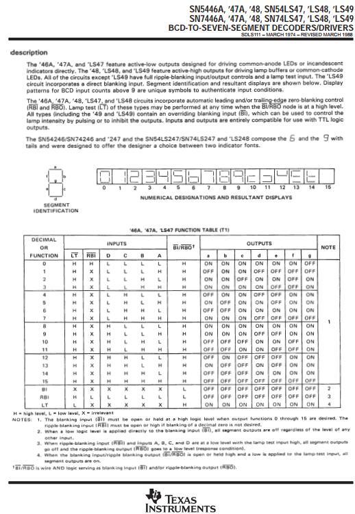
51 Table 1 2. BCD-to-seven Segment converter: A light emitting Diode (LED) is a PN junction diode. When the diode is forward biased, a current flows through the junction and the light is emitted.see Fig.2. A seven segment LED display contains 7 LEDs. Each LED is called a segment and they are identified as (a, b, c, d, e, f, g) segments. Figure 3. The display has 7 inputs each connected to an LED segment. All anodes of LEDs are tied together and joined to 5 volts (this type is called common anode type). A limiting resistance 51
52 network must be used at the inputs to protect the 7-segment from overloading. BCD inputs are converted into 7-segment inputs (a, b, c, d, e, f, g) by using a decoder, as shown in Fig.4. A decoder is a combinational circuit that converts binary information from n input lines to a maximum of 2n output lines. The input to the decoder is a BCD code and the outputs of the systems are the seven segments a, b, c, d, e, f, and g. For further information and pin connections, consult the specification sheet for decoder and 7-segment units. First design a combinational circuit which would simulate the decoder function for only the segment a, of the display. This can be done in the following steps:- a) Write down the truth table with 4 inputs and 7 outputs (Table 2). b) For only the output a, obtain a minimum logic function. Realize this function using NAND gates and inverters only. For example if decimal 9 is to be displayed a, b, c, d, f, g must be 0 and the others must be 1 (For common anode type display units), if decimal 5 is to be displayed then a, f, g, c, d must be 0 and the others must be 1. c) Connect the output a of your circuit to appropriate input of 7-segment display unit. By applying BCD codes verify the displayeddecimal digits for that segment for a of the display. d) Replace your circuit by a decoder IC 7447 for all of the seven segments. Observe the display and record the segments that will light up for invalid inputs sequence. 52
53 e) Comment on the design if you don t want to see any digit for invalid input sequence. 53
54 54
55 55
56 56
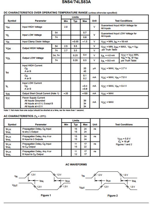
57 EE 200 DIGITAL LOGIC DESIGN EXPERIMENT #7 ADDERS, SUBTRACTORS AND MAGNITUDE COMPARATORS Objectives: To construct and test various adders and subtractor circuits. To construct and test a magnitude comparator circuit. Apparatus: IC type 7486 quad 2-input XOR gates IC type 7408 quad 2-input AND gates IC type 7404 HEX inverter IC type bit binary adder IC type bit magnitude comparator. Theory: See Sections 1-5,4-3,5-2,5-4 of your textbook. a) Addition: IC type 7483 is a 4-bit binary adder with fast carry. The pin assignment is shown in Fig 1. The two 4-bit input binary numbers are A1 through A4 and B1 through B4. The 4-bit sum is obtained from S1 through S4. Ci is the input carry and Co the out carry. This IC can be used as an addersubtractor as a magnitude comparator. b) Subtraction: S3 The subtraction of two binary numbers can be done by taking the 2 s complement of the subtrahend and adding it to the minued. The 2 s complement can be obtained by taking the 1 s 57
58 complement and adding 1. To perform A - B, we complement the four bits of B, add them to the four bits of A, and add 1 to the input carry. This is done as shown in Fig 2. Four XOR gates complement the bits of B when the mode select M = 1 ( because x 1=x ) and leave the bits of B unchanged when M = 0 (because x 0=x) thus, when the mode select M is equal to 1, the input carry Ci is equal to 1 and the sum output is A plus the 2 s complement of B. When M is equal to 0, the input carry is equal to 0 and the sum generates A + B. c) Magnitude comparison The comparison of two numbers is an operation that determines whether one number is greater than, equal to, or less than the other number. The IC 7485 is a 4 bit magnitude comparator. It compares two 4-Bit binary numbers (labeled as A&B) generates an output of 1 at one of three outputs labeled A > B, A < B, A = B. Three inputs are available for cascading comparators. See Fig.3. 58
59 Procedure: a) Design using LogicWorks a half adder circuit using only XOR gates and NAND gates. Then during the Lab construct the circuit and verify its operation. b) b) Design using LogicWorks a full adder circuit using only XOR gates and NAND gates. Then during the Lab construct the circuit and verify its operation. c) Use IC 7483 to add the two 4-bit numbers A and B shown in Table1. In LogicWorks, select the chip and use Binary switches for the bits of the two numbers and the input carry and use Binary Probe for the sum and carry out. Input carry Ci is taken as logic 0. Show that if the input carry is 1, it adds 1 tothe output sum. In the Lab use switches S1-1 to S1-8 for the two numbers and use the SPDT S2 for the input carry Ci. For sum and carry out, use LED-1 to LED-5. 59
60 d) Connect the adder-subtractor circuit as shown in Fig 2. Perform the following operations and record the values of the output sum and the output carry Co. Show that Co =1 when sum exceeds 15. Comment on sum and Co for the subtraction operations when A > B and A < B. e) Use IC7485 to compare the following two 4 bit numbers A and B. Record the outputs in table 3. Note that in LogicWorks you need to connect (A = B) input to logic 1 (as an indication that previous stages are equal in multi-digit numbers) for correct results while this is not necessary for the hardware. f) A magnitude comparator can be constructed by using a subtractor as in Fig 2. and an additional combinational circuit. This is done with a combinational circuit which has 5 inputs S1, S2, S3, S4, and Co, and three outputs X, Y, Z see Fig.4 X = 1 if A = B Where S =
61 Y = 1 if A < B Where Co = 0 Z = 1 if A > B Where Co = 1 S 0000 Design and construct this logic circuit with minimum number of gates. Check the comparator action using Part (e). In the Lab verify your Logic Works simulation. 61
62 62
63 63
64 64
65 EE 200 DIGITAL LOGIC DESIGN EXPERIMENT #8 DESIGN WITH MULTIPLEXERS Objectives To design a combinational circuit and implement it with multiplexers. To use a demultiplexer to implement a multiple output combinational circuit from the same input variables. Apparatus IC type 7404 HEX inverter IC type 7408 quad 2-input AND gate IC type x1 multiplexer (1) IC type dual 4x1 multiplexer (2) IC type 7446 BCD-to-Seven-Segment decoder (1) Resistance network (1) Seven-Segment Display (1) Theory See section 5.6 of your text. IC Description is a 8 line-to-1 line multiplexer. It has the schematic representation shown in Fig 1. Selection lines S2, S1 and S0 select the particular input to be multiplexed and applied to the output. Strobe S acts as an enable signal. If strobe =1, the chip is disabled and output y = 0. If strobe = 0 then the chip is enabled and functions as a multiplexer. Table 1 shows the multiplex function of in terms of select lines is a dual 4 line-to-1 line multiplexer. It has the schematic representation shown in Fig 2. Selection lines S1 and S0 select the particular input to be multiplexed and applied to the output IY{1 = 1, 2}. 65
66 Each of the strobe signals IG {I = 1, 2} acts as an enable signal for the corresponding multiplexer. Table 2. shows the multiplex function of in terms of select lines. Note that each of the on-chip multiplexers act independently from the other, while sharing the same select lines S1 and S0. IC 7446 is a BCD to seven segment decoder driver. It is used to convert the combinational circuit outputs in BCD forms into 7 segment digits for the 7 segment LED display units. See experiment #5. Procedure: Part I: Parity Generator: 66
67 a) Design a parity generator by using a multiplexer. Parity is an extra bit attached to a code to check that the code has been received correctly. Odd parity bit means that the number of 1 s in the code including the parity bit is an odd number. Fill the output column of the truth table in Table 2 for a 5-bit code in which four of the bits (A,B,C,D) represents the information to be sent and fifth bit (x), represents the parity bit. The required parity is an odd parity. The inputs B,C and D correspond to the select inputs of Complete the truth table in Table 3 by filling in the last column with 0,1,A or A. b) Simulate the circuit using LogicWorks, use multiplexer and Binary switches for inputs and Binary Probes for outputs. The has one output for Y and another inverted output W. Use A and A for providing values for inputs 0-7. The internal values A, B, C are used for selection inputs B,C, and D. Simulate the circuit and test each input combination filling in the table shown below. In the Lab connect the circuit and verify the operations. Connect an LED to the multiplexer output so that it represents the parity bit which lights any time when the four bits input have even parity. Part 2: Vote Counter: A committee is composed of a chairman (C), a senior member (S), and a member (M). The rules of the committee state that: The vote of the member (M) will be counted as 2 votes The vote of the senior member will be counted as 3 votes. 67
68 The vote of the chairman will be counted as 5 votes. Each of these persons has a switch to close ( l ) when voting yes and to open ( 0 ) when voting no. It is necessary to design a circuit that displays the total number of votes for each issue. Use a seven segment display and a decoder to display the required number. If all members vote no for an issue the display should be blank. (Recall from Experiment #5, that a binary input 15 into the 7446 blanks all seven segments). If all members vote yes for an issue, the display should be 0. Otherwise the display shows a decimal number equal to the number of 'yes' votes. Use two units, which include four multiplexers to design the combinational circuit that converts the inputs from the members switch to the BCD digit for the In LogicWorks use +5V for Logic 1 and ground for Logic 0 and use switches for C, S, and M. Use two chips and one decoder 7446 verify your design and get a copy of your circuit with the pin numbers to Lab so that you could connect the hardware in exactly the same way. 68
69 69
70 70
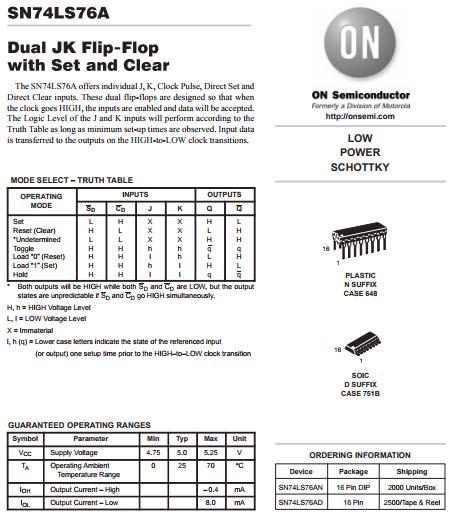
71 EE 200 DIGITAL LOGIC DESIGN EXPERIMENT #9 FLIP-FLOPS Objectives 1. To become familiar with flip-flops. 2. To implement and observe the operation of different flip-flops. Apparatus IC type 7400 quad 2-input NAND gate IC type 7410 triple 3- input NAND gate IC type 7476 dual JK master-slave flip-flops. IC type 7474 dual D positive-edge-trigged flip-flops. Dual trace oscilloscope. Theory See sections 6-2 and 6-3 of your text. Procedure 1. In the pre-lab using LogicWorks construct the circuit shown in Fig.1 Where we could use generic NAND gates or and Binary Probes to simulate LEDs. Finally, we use SPDT for the bouncing switch. Using the simulated circuit fill in the truth table. 71
72 In the Lab, Build the RS latch shown in fig.2. Use SPDT switch S2 as a bouncing switch. Q and Q Outputs are connected to LED S of the PB-503. Verify the truth table experimentally. 2. Modify the basic R-S into a D latch by adding the steering gates and the inverter shown in Fig 3. Connect the D input to the pulse generator of the digi designer and set it at 1 Hz. Connect the enable input to a high through 1k resistor. Observe the output; obtain the truth table experimentally then change the enable to a low. Is the enable an active high or an active? Leave the enable low and place a momentary short to ground first on one output and then on the other. What happens? 72
73 3. The 7476 is a dual JK master-slave flip-flops with preset and clear inputs. The function table given in table 1 defines the operation of the flip-flop. The +ve transition of the CLOCK (CP) pulse changes the master flip-flop, and the (-ve) transition changes the slave flip-flop as well as the output of the circuit. In LogicWorks the chip 7476 is not available, however, the generic JK flip-flop behave in exactly the same way as the The S represents the Preset, the R represents the Clear, and C represents the clock pulse (CP). Verify the table by connecting Binary switches to R, S, J, K, and C. Notice that only the negative edge of the clock affects the outputs (Q, and Q ). 73
74 In the Lab, Construct the circuit of Fig 4. Look at the data sheet for the 7476 and determine the inactive logic required at the PRE and CLR inputs. Connect the 7476 for the SET mode by connecting J = 1, K = 0. With CLOCK (CP) = 0; test the effect of PRE, CLR by putting a 0 on each, one at a time. Put CLR = 0, then pulse the clock (CP) by putting a HIGH then a LOW, on the clock. Does the CLR input override J input? Verify the operation of the JK flip flop by experimentally obtaining the characteristics. 74
75 75
76 76
77 77
78 EE 200 DIGITAL LOGIC DESIGN EXPERIMENT #10 CLOCKED SEQUENTIAL CIRCUITS AND COUNTERS OBJECTIVE To design, build and test synchronous sequential circuits. To design, build, and test synchronous counters To design, build and test asynchronous counters APPARATUS IC type 7476 dual JK master-slave flip-flops IC type 7400 quad 2-input NAND gates THEORY See sections 6-6, 6-7, 6-8, 7.2 and 7.5 of your own text. PROCEDURE 1. SYNCHRONOUS SEQUENTIAL CIRCUITS a). Design, construct and test a sequential circuit whose state is shown in Fig.1. Use JK flipflops in the design. 78
79 The circuit has two flip-flops A, B, one input x and one output y. The circuit is to be designed by treating the unused states as don t care conditions. The final circuit must be analyzed to ensure that it is self-correcting. If not suggest a solution. b) Complete the excitation table shown in Table 1. c) Using Karnaugh maps obtain minimal expressions for the flip-flop input functions JA,, KC d) Simulate the circuit using LogicWorks. LogicWorks does not have the JK master-slave flipflop IC Use instead the generic JK flip-flop as you did in experiment 9. In the Lab, build the circuit and check the output to verify the state table values. 2. Synchronous Counters Synchronous counters have all clock lines tied to a common clock causing all flip-flops to change at the same time. The count sequence of a counter can be analysed by placing the counter into every possible number in the sequence and determining the next number in the sequence state diagram is developed as the analysis proceeds. (A state diagram is an illustration of the transitions that occur after each clock pulse). a) In the pre-lab using LogicWorks and then in the lab using hardware chips, design a 2-bit gray code counter using JK flip-flops. The required sequence is the binary equivalent of ( ). A state diagram for this counter is given in Fig
80 b) Complete the excitation table (Table 2) for the counter and obtain logic expression for the JK flip-flop input functions. c) In the lab, build the circuit and test it by pulsing it from the PB-503. Check that the output is the designed sequence. 3. A Synchronous Counters Asynchronous counters are a series of flip-flops each clocked by the previous state, one after the other. Since all the stages of the counter are not clocked together, a ripple effect propagates as various flip-flops are clocked. For this reason they are called ripple counters. The modulus of a counter is the number of different output states the counter may take (i.e. Mod 4 means the counter has four output states). 80
81 a) In the pre-lab construct a 4-bit asynchronous counter shown in Fig.3. (It is also called binary ripple counter). Use four generic JK flip-flops. Connect four Binary Probes to Q outputs. Connect all R and S inputs to Logic 1 and connect a switch to the CP input. b) In the Lab use two 7476 ICs to implement the design. Connect Q outputs of flip-flops to indicator lamps of the PB-503. Connect all clear (CLR) and preset (PRE) inputs to logic 1. Connect the CP input to the pulse output of the PB-503 and check the counter for proper operation. c) Write down the count sequence in Table 3. Identify this count sequence (up or down). Comment on what happens after the application of 15 pulses to CP input. 81
MODULAR DIGITAL ELECTRONICS TRAINING SYSTEM
 MODULAR DIGITAL ELECTRONICS TRAINING SYSTEM MDETS UCTECH's Modular Digital Electronics Training System is a modular course covering the fundamentals, concepts, theory and applications of digital electronics.
EE 210. LOGIC DESIGN LAB.
 College of Engineering Electrical Engineering Department EE 210. LOGIC DESIGN LAB. (1 st semester 1426-27) Dr. Messaoud Boukezzata Office: EE 11 Phone: 063 8000 50 Ext 3152 1 College of Engineering Electrical
North Shore Community College
 North Shore Community College Course Number: IEL217 Section: MAL Course Name: Digital Electronics 1 Semester: Credit: 4 Hours: Three hours of Lecture, Two hours Laboratory per week Thursdays 8:00am (See
NORTHWESTERN UNIVERSITY TECHNOLOGICAL INSTITUTE
 NORTHWESTERN UNIVERSITY TECHNOLOGICL INSTITUTE ECE 270 Experiment #8 DIGITL CIRCUITS Prelab 1. Draw the truth table for the S-R Flip-Flop as shown in the textbook. Draw the truth table for Figure 7. 2.
Physics 323. Experiment # 10 - Digital Circuits
 Physics 323 Experiment # 10 - Digital Circuits Purpose This is a brief introduction to digital (logic) circuits using both combinational and sequential logic. The basic building blocks will be the Transistor
MODULE 3. Combinational & Sequential logic
 MODULE 3 Combinational & Sequential logic Combinational Logic Introduction Logic circuit may be classified into two categories. Combinational logic circuits 2. Sequential logic circuits A combinational
MODU LE DAY. Class-A, B, AB and C amplifiers - basic concepts, power, efficiency Basic concepts of Feedback and Oscillation. Day 1
 DAY MODU LE TOPIC QUESTIONS Day 1 Day 2 Day 3 Day 4 I Class-A, B, AB and C amplifiers - basic concepts, power, efficiency Basic concepts of Feedback and Oscillation Phase Shift Wein Bridge oscillators.
St. MARTIN S ENGINEERING COLLEGE
 St. MARTIN S ENGINEERING COLLEGE Dhulapally, Kompally, Secunderabad-500014. Branch Year&Sem Subject Name : Electronics and Communication Engineering : II B. Tech I Semester : SWITCHING THEORY AND LOGIC
SEMESTER ONE EXAMINATIONS 2002
 SEMESTER ONE EXAMINATIONS 2002 EE101 Digital Electronics Solutions Question 1. An assembly line has 3 failsafe sensors and 1 emergency shutdown switch. The Line should keep moving unless any of the following
DEPARTMENT OF COMPUTER SCIENCE & ENGINEERING
 DRONACHARYA GROUP OF INSTITUTIONS, GREATER NOIDA Affiliated to Mahamaya Technical University, Noida Approved by AICTE DEPARTMENT OF COMPUTER SCIENCE & ENGINEERING Lab Manual for Computer Organization Lab
Find the equivalent decimal value for the given value Other number system to decimal ( Sample)
") VELAMMAL COLLEGE OF ENGINEERING AND TECHNOLOGY, MADURAI 65 009 Department of Information Technology Model Exam-II-Question bank PART A (Answer for all Questions) (8 X = 6) K CO Marks Find the equivalent
VELAMMAL COLLEGE OF ENGINEERING AND TECHNOLOGY, MADURAI 65 009 Department of Information Technology Model Exam-II-Question bank PART A (Answer for all Questions) (8 X = 6) K CO Marks Find the equivalent
CPE 200L LABORATORY 3: SEQUENTIAL LOGIC CIRCUITS UNIVERSITY OF NEVADA, LAS VEGAS GOALS: BACKGROUND: SR FLIP-FLOP/LATCH
 CPE 200L LABORATORY 3: SEUENTIAL LOGIC CIRCUITS DEPARTMENT OF ELECTRICAL AND COMPUTER ENGINEERING UNIVERSITY OF NEVADA, LAS VEGAS GOALS: Learn to use Function Generator and Oscilloscope on the breadboard.
The word digital implies information in computers is represented by variables that take a limited number of discrete values.
 Class Overview Cover hardware operation of digital computers. First, consider the various digital components used in the organization and design. Second, go through the necessary steps to design a basic
R13 SET - 1 '' ''' '' ' '''' Code No: RT21053
 SET - 1 1. a) What are the characteristics of 2 s complement numbers? b) State the purpose of reducing the switching functions to minimal form. c) Define half adder. d) What are the basic operations in
MODEL QUESTIONS WITH ANSWERS THIRD SEMESTER B.TECH DEGREE EXAMINATION DECEMBER CS 203: Switching Theory and Logic Design. Time: 3 Hrs Marks: 100
 MODEL QUESTIONS WITH ANSWERS THIRD SEMESTER B.TECH DEGREE EXAMINATION DECEMBER 2016 CS 203: Switching Theory and Logic Design Time: 3 Hrs Marks: 100 PART A ( Answer All Questions Each carries 3 Marks )
1. Convert the decimal number to binary, octal, and hexadecimal.
 1. Convert the decimal number 435.64 to binary, octal, and hexadecimal. 2. Part A. Convert the circuit below into NAND gates. Insert or remove inverters as necessary. Part B. What is the propagation delay
PHYSICS 5620 LAB 9 Basic Digital Circuits and Flip-Flops
 PHYSICS 5620 LAB 9 Basic Digital Circuits and Flip-Flops Objective Construct a two-bit binary decoder. Study multiplexers (MUX) and demultiplexers (DEMUX). Construct an RS flip-flop from discrete gates.
WINTER 15 EXAMINATION Model Answer
 Important Instructions to examiners: 1) The answers should be examined by key words and not as word-to-word as given in the model answer scheme. 2) The model answer and the answer written by candidate
Department of Computer Science and Engineering Question Bank- Even Semester:
 Department of Computer Science and Engineering Question Bank- Even Semester: 2014-2015 CS6201& DIGITAL PRINCIPLES AND SYSTEM DESIGN (Common to IT & CSE, Regulation 2013) UNIT-I 1. Convert the following
OFC & VLSI SIMULATION LAB MANUAL
 DEVBHOOMI INSTITUTE OF TECHNOLOGY FOR WOMEN, DEHRADUN - 24847 DEPARTMENT OF ELECTRONICS AND COMMUNICATION ENGINEERING Prepared BY: Ajay Kumar Gautam Asst. Prof. Electronics & Communication Engineering
ME 515 Mechatronics. Introduction to Digital Electronics
 ME 55 Mechatronics /5/26 ME 55 Mechatronics Digital Electronics Asanga Ratnaweera Department of Faculty of Engineering University of Peradeniya Tel: 8239 (3627) Email: asangar@pdn.ac.lk Introduction to
DepartmentofElectronicEngineering NEDUniversity ofengineering &Technology LABORATORY WORKBOOK DIGITAL LOGIC DESIGN (TC-201)
") DepartmentofElectronicEngineering NEDUniversity ofengineering &Technology LABORATORY WORKBOOK DIGITAL LOGIC DESIGN (TC-201) Instructor Name: Student Name: Roll Number: Semester: Batch: Year: Department:
DepartmentofElectronicEngineering NEDUniversity ofengineering &Technology LABORATORY WORKBOOK DIGITAL LOGIC DESIGN (TC-201) Instructor Name: Student Name: Roll Number: Semester: Batch: Year: Department:
TIME SCHEDULE. MODULE TOPICS PERIODS 1 Number system & Boolean algebra 17 Test I 1 2 Logic families &Combinational logic
 COURSE TITLE : DIGITAL INSTRUMENTS PRINCIPLE COURSE CODE : 3075 COURSE CATEGORY : B PERIODS/WEEK : 4 PERIODS/SEMESTER : 72 CREDITS : 4 TIME SCHEDULE MODULE TOPICS PERIODS 1 Number system & Boolean algebra
R13. II B. Tech I Semester Regular Examinations, Jan DIGITAL LOGIC DESIGN (Com. to CSE, IT) PART-A
 PART-A") SET - 1 Note: Question Paper consists of two parts (Part-A and Part-B) Answer ALL the question in Part-A Answer any THREE Questions from Part-B a) What are the characteristics of 2 s complement numbers?
SET - 1 Note: Question Paper consists of two parts (Part-A and Part-B) Answer ALL the question in Part-A Answer any THREE Questions from Part-B a) What are the characteristics of 2 s complement numbers?
DIGITAL SYSTEM DESIGN UNIT I (2 MARKS)
") DIGITAL SYSTEM DESIGN UNIT I (2 MARKS) 1. Convert Binary number (111101100) 2 to Octal equivalent. 2. Convert Binary (1101100010011011) 2 to Hexadecimal equivalent. 3. Simplify the following Boolean function
DIGITAL SYSTEM DESIGN UNIT I (2 MARKS) 1. Convert Binary number (111101100) 2 to Octal equivalent. 2. Convert Binary (1101100010011011) 2 to Hexadecimal equivalent. 3. Simplify the following Boolean function
ECE Lab 5. MSI Circuits - Four-Bit Adder/Subtractor with Decimal Output
 ECE 201 - Lab 5 MSI Circuits - Four-Bit Adder/Subtractor with Decimal Output PURPOSE To familiarize students with Medium Scale Integration (MSI) technology, specifically adders. The student should also
Computer Architecture and Organization
 A-1 Appendix A - Digital Logic Computer Architecture and Organization Miles Murdocca and Vincent Heuring Appendix A Digital Logic A-2 Appendix A - Digital Logic Chapter Contents A.1 Introduction A.2 Combinational
CHAPTER 4: Logic Circuits
 CHAPTER 4: Logic Circuits II. Sequential Circuits Combinational circuits o The outputs depend only on the current input values o It uses only logic gates, decoders, multiplexers, ALUs Sequential circuits
Analogue Versus Digital [5 M]
![Analogue Versus Digital [5 M]](/thumbs/93/111640168.jpg "Analogue Versus Digital [5 M]") Q.1 a. Analogue Versus Digital [5 M] There are two basic ways of representing the numerical values of the various physical quantities with which we constantly deal in our day-to-day lives. One of the ways,
Q.1 a. Analogue Versus Digital [5 M] There are two basic ways of representing the numerical values of the various physical quantities with which we constantly deal in our day-to-day lives. One of the ways,
MC9211 Computer Organization
 MC9211 Computer Organization Unit 2 : Combinational and Sequential Circuits Lesson2 : Sequential Circuits (KSB) (MCA) (2009-12/ODD) (2009-10/1 A&B) Coverage Lesson2 Outlines the formal procedures for the
Electrical and Telecommunications Engineering Technology_TCET3122/TC520. NEW YORK CITY COLLEGE OF TECHNOLOGY The City University of New York
 NEW YORK CITY COLLEGE OF TECHNOLOGY The City University of New York DEPARTMENT: SUBJECT CODE AND TITLE: COURSE DESCRIPTION: REQUIRED: Electrical and Telecommunications Engineering Technology TCET 3122/TC
Digital Fundamentals. Lab 5 Latches & Flip-Flops CETT Name: Date:
 Richland College School of Engineering & Technology Rev. 0 B. Donham Rev. 1 (7/2003) J. Horne Rev. 2 (1/2008) J. Bradbury Rev. 3 (7/2015) J. Bradbury Digital Fundamentals CETT 1425 Lab 5 Latches & Flip-Flops
EXPERIMENT: 1. Graphic Symbol: OR: The output of OR gate is true when one of the inputs A and B or both the inputs are true.
 EXPERIMENT: 1 DATE: VERIFICATION OF BASIC LOGIC GATES AIM: To verify the truth tables of Basic Logic Gates NOT, OR, AND, NAND, NOR, Ex-OR and Ex-NOR. APPARATUS: mention the required IC numbers, Connecting
Chapter 4. Logic Design
 Chapter 4 Logic Design 4.1 Introduction. In previous Chapter we studied gates and combinational circuits, which made by gates (AND, OR, NOT etc.). That can be represented by circuit diagram, truth table
Department of CSIT. Class: B.SC Semester: II Year: 2013 Paper Title: Introduction to logics of Computer Max Marks: 30
 Department of CSIT Class: B.SC Semester: II Year: 2013 Paper Title: Introduction to logics of Computer Max Marks: 30 Section A: (All 10 questions compulsory) 10X1=10 Very Short Answer Questions: Write
UNIT 1: DIGITAL LOGICAL CIRCUITS What is Digital Computer? OR Explain the block diagram of digital computers.
 UNIT 1: DIGITAL LOGICAL CIRCUITS What is Digital Computer? OR Explain the block diagram of digital computers. Digital computer is a digital system that performs various computational tasks. The word DIGITAL
DIGITAL LOGIC DESIGN. Press No: 42. Second Edition
 DIGITAL LOGIC DESIGN DIGITAL LOGIC DESIGN Press No: 42 Second Edition Qafqaz University Press Bakı - 2010 Ministry of Education of Azerbaijan Republic Institute of Educational Problems Çağ Educational
Dev Bhoomi Institute Of Technology Department of Electronics and Communication Engineering PRACTICAL INSTRUCTION SHEET
 Dev Bhoomi Institute Of Technology Department of Electronics and Communication Engineering PRACTICAL INSTRUCTION SHEET LABORATORY MANUAL EXPERIMENT NO. 1 ISSUE NO. : ISSUE DATE: REV. NO. : REV. DATE :
Laboratory Objectives and outcomes for Digital Design Lab
 Class: SE Department of Information Technology Subject Logic Design Sem : III Course Objectives and outcomes for LD Course Objectives: Students will try to : COB1 Understand concept of various components.
DIGITAL ELECTRONICS LAB MANUAL FOR 2/4 B.Tech (ECE) COURSE CODE: EC-252
 COURSE CODE: EC-252") DIGITAL ELECTRONICS LAB MANUAL FOR /4 B.Tech (ECE) COURSE CODE: EC-5 PREPARED BY P.SURENDRA KUMAR M.TECH, Lecturer D.SWETHA M.TECH, Lecturer T Srinivasa Rao M.TECH, Lecturer Ch.Madhavi, Lab Assistant 009-00
DIGITAL ELECTRONICS LAB MANUAL FOR /4 B.Tech (ECE) COURSE CODE: EC-5 PREPARED BY P.SURENDRA KUMAR M.TECH, Lecturer D.SWETHA M.TECH, Lecturer T Srinivasa Rao M.TECH, Lecturer Ch.Madhavi, Lab Assistant 009-00
TYPICAL QUESTIONS & ANSWERS
 DIGITALS ELECTRONICS TYPICAL QUESTIONS & ANSWERS OBJECTIVE TYPE QUESTIONS Each Question carries 2 marks. Choose correct or the best alternative in the following: Q.1 The NAND gate output will be low if
Digital Principles and Design
 Digital Principles and Design Donald D. Givone University at Buffalo The State University of New York Grauu Boston Burr Ridge, IL Dubuque, IA Madison, Wl New York San Francisco St. Louis Bangkok Bogota
Solution to Digital Logic )What is the magnitude comparator? Design a logic circuit for 4 bit magnitude comparator and explain it,
What is the magnitude comparator? Design a logic circuit for 4 bit magnitude comparator and explain it,") Solution to Digital Logic -2067 Solution to digital logic 2067 1.)What is the magnitude comparator? Design a logic circuit for 4 bit magnitude comparator and explain it, A Magnitude comparator is a combinational
Solution to Digital Logic -2067 Solution to digital logic 2067 1.)What is the magnitude comparator? Design a logic circuit for 4 bit magnitude comparator and explain it, A Magnitude comparator is a combinational
University of Victoria. Department of Electrical and Computer Engineering. CENG 290 Digital Design I Lab Manual
 University of Victoria Department of Electrical and Computer Engineering CENG 290 Digital Design I Lab Manual INDEX Introduction to the labs Lab1: Digital Instrumentation Lab2: Basic Digital Components
EE292: Fundamentals of ECE
 EE292: Fundamentals of ECE Fall 2012 TTh 10:00-11:15 SEB 1242 Lecture 23 121120 http://www.ee.unlv.edu/~b1morris/ee292/ 2 Outline Review Combinatorial Logic Sequential Logic 3 Combinatorial Logic Circuits
UNIVERSITY OF MASSACHUSSETS LOWELL Department of Electrical & Computer Engineering Course Syllabus for Logic Design Fall 2013
 UNIVERSITY OF MASSACHUSSETS LOWELL Department of Electrical & Computer Engineering Course Syllabus for 16.265 Logic Design Fall 2013 I. General Information Section 201 Instructor: Professor Anh Tran Office
UNIT III. Combinational Circuit- Block Diagram. Sequential Circuit- Block Diagram
 UNIT III INTRODUCTION In combinational logic circuits, the outputs at any instant of time depend only on the input signals present at that time. For a change in input, the output occurs immediately. Combinational
YEDITEPE UNIVERSITY DEPARTMENT OF COMPUTER ENGINEERING. EXPERIMENT VIII: FLIP-FLOPS, COUNTERS 2014 Fall
 YEDITEPE UNIVERSITY DEPARTMENT OF COMPUTER ENGINEERING EXPERIMENT VIII: FLIP-FLOPS, COUNTERS 2014 Fall Objective: - Dealing with the operation of simple sequential devices. Learning invalid condition in
Introduction to Digital Electronics
 Introduction to Digital Electronics by Agner Fog, 2018-10-15. Contents 1. Number systems... 3 1.1. Decimal, binary, and hexadecimal numbers... 3 1.2. Conversion from another number system to decimal...
Chapter Contents. Appendix A: Digital Logic. Some Definitions
 A- Appendix A - Digital Logic A-2 Appendix A - Digital Logic Chapter Contents Principles of Computer Architecture Miles Murdocca and Vincent Heuring Appendix A: Digital Logic A. Introduction A.2 Combinational
Digital Circuits I and II Nov. 17, 1999
 Physics 623 Digital Circuits I and II Nov. 17, 1999 Digital Circuits I 1 Purpose To introduce the basic principles of digital circuitry. To understand the small signal response of various gates and circuits
UNIT-3: SEQUENTIAL LOGIC CIRCUITS
 UNIT-3: SEQUENTIAL LOGIC CIRCUITS STRUCTURE 3. Objectives 3. Introduction 3.2 Sequential Logic Circuits 3.2. NAND Latch 3.2.2 RS Flip-Flop 3.2.3 D Flip-Flop 3.2.4 JK Flip-Flop 3.2.5 Edge Triggered RS Flip-Flop
INSTITUTE OF AERONAUTICAL ENGINEERING (Autonomous) Dundigal, Hyderabad ELECTRICAL AND ELECTRONICS ENGINEERING
 Dundigal, Hyderabad ELECTRICAL AND ELECTRONICS ENGINEERING") Course Name INSTITUTE OF AERONAUTICAL ENGINEERING (Autonomous) Dundigal, Hyderabad - 500 043 ELECTRICAL AND ELECTRONICS ENGINEERING QUESTION BANK : SWITCHING THEORY AND LOGIC DESISN Course Code : A40407
Course Name INSTITUTE OF AERONAUTICAL ENGINEERING (Autonomous) Dundigal, Hyderabad - 500 043 ELECTRICAL AND ELECTRONICS ENGINEERING QUESTION BANK : SWITCHING THEORY AND LOGIC DESISN Course Code : A40407
RAO PAHALD SINGH GROUP OF INSTITUTIONS BALANA(MOHINDER GARH)123029
123029") DIGITAL ELECTRONICS LAB( EE-224-F) DIGITAL ELECTRONICS LAB (EE-224-F) LAB MANUAL IV SEMESTER RAO PAHALD SINGH GROUP OF INSTITUTIONS BALANA(MOHINDER GARH)2329 Department Of Electronics & Communication Engg.
DIGITAL ELECTRONICS LAB( EE-224-F) DIGITAL ELECTRONICS LAB (EE-224-F) LAB MANUAL IV SEMESTER RAO PAHALD SINGH GROUP OF INSTITUTIONS BALANA(MOHINDER GARH)2329 Department Of Electronics & Communication Engg.
MAHARASHTRA STATE BOARD OF TECHNICAL EDUCATION (Autonomous) (ISO/IEC Certified) WINTER 2018 EXAMINATION MODEL ANSWER
 (ISO/IEC Certified) WINTER 2018 EXAMINATION MODEL ANSWER") Important Instructions to examiners: 1) The answers should be examined by key words and not as word-to-word as given in themodel answer scheme. 2) The model answer and the answer written by candidate may
Important Instructions to examiners: 1) The answers should be examined by key words and not as word-to-word as given in themodel answer scheme. 2) The model answer and the answer written by candidate may
Subject : EE6301 DIGITAL LOGIC CIRCUITS
 QUESTION BANK Programme : BE Subject : Semester / Branch : III/EEE UNIT 1 NUMBER SYSTEMS AND DIGITAL LOGIC FAMILIES Review of number systems, binary codes, error detection and correction codes (Parity
Principles of Computer Architecture. Appendix A: Digital Logic
 A-1 Appendix A - Digital Logic Principles of Computer Architecture Miles Murdocca and Vincent Heuring Appendix A: Digital Logic A-2 Appendix A - Digital Logic Chapter Contents A.1 Introduction A.2 Combinational
Decade Counters Mod-5 counter: Decade Counter:
 Decade Counters We can design a decade counter using cascade of mod-5 and mod-2 counters. Mod-2 counter is just a single flip-flop with the two stable states as 0 and 1. Mod-5 counter: A typical mod-5
CHAPTER 4: Logic Circuits
 CHAPTER 4: Logic Circuits II. Sequential Circuits Combinational circuits o The outputs depend only on the current input values o It uses only logic gates, decoders, multiplexers, ALUs Sequential circuits
Tribhuvan University Institute of Science and Technology Bachelor of Science in Computer Science and Information Technology
 Tribhuvan University Institute of Science and Technology Bachelor of Science in Computer Science and Information Technology Course Title: Digital Logic Full Marks: 60 + 0 + 0 Course No.: CSC Pass Marks:
CS302 Digital Logic Design Solved Objective Midterm Papers For Preparation of Midterm Exam
 CS302 Digital Logic Design Solved Objective Midterm Papers For Preparation of Midterm Exam MIDTERM EXAMINATION Spring 2012 Question No: 1 ( Marks: 1 ) - Please choose one A SOP expression is equal to 1
 UNIT 1 NUMBER SYSTEMS AND DIGITAL LOGIC FAMILIES 1. Briefly explain the stream lined method of converting binary to decimal number with example. 2. Give the Gray code for the binary number (111) 2. 3.
Minnesota State College Southeast
 ELEC 2211: Digital Electronics II A. COURSE DESCRIPTION Credits: 4 Lecture Hours/Week: 2 Lab Hours/Week: 4 OJT Hours/Week: *.* Prerequisites: None Corequisites: None MnTC Goals: None Minnesota State College
Logic Design Viva Question Bank Compiled By Channveer Patil
 Logic Design Viva Question Bank Compiled By Channveer Patil Title of the Practical: Verify the truth table of logic gates AND, OR, NOT, NAND and NOR gates/ Design Basic Gates Using NAND/NOR gates. Q.1
Light Emitting Diodes and Digital Circuits I
 LED s and Digital Circuits I. p. 1 Light Emitting Diodes and Digital Circuits I Tasks marked by an asterisk (*) may be carried out before coming to the lab. The Light Emitting Diode: The light emitting
EXPERIMENT 13 ITERATIVE CIRCUITS
 EE 2449 Experiment 13 Revised 4/17/2017 CALIFORNIA STATE UNIVERSITY LOS ANGELES Department of Electrical and Computer Engineering EE-246 Digital Logic Lab EXPERIMENT 13 ITERATIVE CIRCUITS Text: Mano, Digital
Sequential Digital Design. Laboratory Manual. Experiment #3. Flip Flop Storage Elements
 The Islamic University of Gaza Engineering Faculty Department of Computer Engineering Spring 2018 ECOM 2022 Khaleel I. Shaheen Sequential Digital Design Laboratory Manual Experiment #3 Flip Flop Storage
VU Mobile Powered by S NO Group
 Question No: 1 ( Marks: 1 ) - Please choose one A 8-bit serial in / parallel out shift register contains the value 8, clock signal(s) will be required to shift the value completely out of the register.
Lab #6: Combinational Circuits Design
 Lab #6: Combinational Circuits Design PURPOSE: The purpose of this laboratory assignment is to investigate the design of combinational circuits using SSI circuits. The combinational circuits being implemented
10.1 Sequential logic circuits are a type of logic circuit where the output of the circuit depends not only on
 CALIFORNIA STATE UNIVERSITY LOS ANGELES Department of Electrical and Computer Engineering EE-2449 Digital Logic Lab EXPERIMENT 10 INTRODUCTION TO SEQUENTIAL LOGIC EE 2449 Experiment 10 nwp & jgl 1/1/18
[2 credit course- 3 hours per week]
![[2 credit course- 3 hours per week]](/thumbs/94/121292011.jpg "[2 credit course- 3 hours per week]") Syllabus of Applied Electronics for F Y B Sc Semester- 1 (With effect from June 2012) PAPER I: Components and Devices [2 credit course- 3 hours per week] Unit- I : CIRCUIT THEORY [10 Hrs] Introduction;
Syllabus of Applied Electronics for F Y B Sc Semester- 1 (With effect from June 2012) PAPER I: Components and Devices [2 credit course- 3 hours per week] Unit- I : CIRCUIT THEORY [10 Hrs] Introduction;
Light Emitting Diodes and Digital Circuits I
 LED s and Digital Circuits I. p. 1 Light Emitting Diodes and Digital Circuits I Tasks marked by an asterisk (*) may be carried out before coming to the lab. The Light Emitting Diode: The light emitting
Code No: A R09 Set No. 2
 Code No: A109210503 R09 Set No. 2 II B.Tech I Semester Examinations,November 2010 DIGITAL LOGIC DESIGN Computer Science And Engineering Time: 3 hours Max Marks: 75 Answer any FIVE Questions All Questions
Combinational Logic Design
 Lab #2 Combinational Logic Design Objective: To introduce the design of some fundamental combinational logic building blocks. Preparation: Read the following experiment and complete the circuits where
Engineering College. Electrical Engineering Department. Digital Electronics Lab
 Engineering College Electrical Engineering Department Digital Electronics Lab Prepared by: Dr. Samer Mayaleh Eng. Nuha Odeh 2009/2010-1 - CONTENTS Experiment Name Page 1- Measurement of Basic Logic Gates
Name: Date: Suggested Reading Chapter 7, Digital Systems, Principals and Applications; Tocci
 Richland College Engineering Technology Rev. 0 B. Donham Rev. 1 (7/2003) J. Horne Rev. 2 (1/2008) J. Bradbury Digital Fundamentals CETT 1425 Lab 7 Asynchronous Ripple Counters Name: Date: Objectives: To
PHY 351/651 LABORATORY 9 Digital Electronics The Basics
 PHY 351/651 LABORATORY 9 Digital Electronics The Basics Reading Assignment Horowitz, Hill Chap. 8 Data sheets 74HC10N, 74HC86N, 74HC04N, 74HC03N, 74HC32N, 74HC08N, CD4007UBE, 74HC76N, LM555 Overview Over
DIGITAL ELECTRONICS: LOGIC AND CLOCKS
 DIGITL ELECTRONICS: LOGIC ND CLOCKS L 6 INTRO: INTRODUCTION TO DISCRETE DIGITL LOGIC, MEMORY, ND CLOCKS GOLS In this experiment, we will learn about the most basic elements of digital electronics, from
DIGITAL SYSTEM FUNDAMENTALS (ECE421) DIGITAL ELECTRONICS FUNDAMENTAL (ECE422) COUNTERS
 DIGITAL ELECTRONICS FUNDAMENTAL (ECE422) COUNTERS") COURSE / CODE DIGITAL SYSTEM FUNDAMENTALS (ECE421) DIGITAL ELECTRONICS FUNDAMENTAL (ECE422) COUNTERS One common requirement in digital circuits is counting, both forward and backward. Digital clocks and
COURSE / CODE DIGITAL SYSTEM FUNDAMENTALS (ECE421) DIGITAL ELECTRONICS FUNDAMENTAL (ECE422) COUNTERS One common requirement in digital circuits is counting, both forward and backward. Digital clocks and
Chapter 9 Introduction to Sequential Logic
 Chapter 9 Introduction to Sequential Logic Chapter Objectives Upon successful completion of this chapter, you will be able to: Explain the difference between combinational and sequential circuits. Define
Lab #10 Hexadecimal-to-Seven-Segment Decoder, 4-bit Adder-Subtractor and Shift Register. Fall 2017
 University of Texas at El Paso Electrical and Computer Engineering Department EE 2169 Laboratory for Digital Systems Design I Lab #10 Hexadecimal-to-Seven-Segment Decoder, 4-bit Adder-Subtractor and Shift
1.b. Realize a 5-input NOR function using 2-input NOR gates only.
 . [3 points] Short Questions.a. Prove or disprove that the operators (,XOR) form a complete set. Remember that the operator ( ) is implication such that: A B A B.b. Realize a 5-input NOR function using
WINTER 14 EXAMINATION
 Subject Code: 17320 WINTER 14 EXAMINATION Model Answer Important Instructions to examiners: 1) The answers should be examined by key words and not as word-to-word as given in the model answer scheme. 2)
DIGITAL ELECTRONICS MCQs
 DIGITAL ELECTRONICS MCQs 1. A 8-bit serial in / parallel out shift register contains the value 8, clock signal(s) will be required to shift the value completely out of the register. A. 1 B. 2 C. 4 D. 8
MAHARASHTRA STATE BOARD OF TECHNICAL EDUCATION (Autonomous) (ISO/IEC Certified)
 (ISO/IEC Certified)") Important Instructions to examiners: 1) The answers should be examined by key words and not as word-to-word as given in the model answer scheme. 2) The model answer and the answer written by candidate
Important Instructions to examiners: 1) The answers should be examined by key words and not as word-to-word as given in the model answer scheme. 2) The model answer and the answer written by candidate
Chapter 3: Sequential Logic Systems
 Chapter 3: Sequential Logic Systems 1. The S-R Latch Learning Objectives: At the end of this topic you should be able to: design a Set-Reset latch based on NAND gates; complete a sequential truth table
Bachelor Level/ First Year/ Second Semester/ Science Full Marks: 60 Computer Science and Information Technology (CSc. 151) Pass Marks: 24
 Pass Marks: 24") 2065 Computer Science and Information Technology (CSc. 151) Pass Marks: 24 Time: 3 hours. Candidates are required to give their answers in their own words as for as practicable. Attempt any TWO questions:
2065 Computer Science and Information Technology (CSc. 151) Pass Marks: 24 Time: 3 hours. Candidates are required to give their answers in their own words as for as practicable. Attempt any TWO questions:
NEW MEXICO STATE UNIVERSITY Electrical and Computer Engineering Department. EE162 Digital Circuit Design Fall Lab 5: Latches & Flip-Flops
 NEW MEXICO STATE UNIVERSITY Electrical and Computer Engineering Department EE162 Digital Circuit Design Fall 2012 OBJECTIVES: Lab 5: Latches & Flip-Flops The objective of this lab is to examine and understand
University of Illinois at Urbana-Champaign
 University of Illinois at Urbana-Champaign Digital Electronics Laboratory Physics Department Physics 40 Laboratory Experiment 3: CMOS Digital Logic. Introduction The purpose of this lab is to continue
CS6201 UNIT I PART-A. Develop or build the following Boolean function with NAND gate F(x,y,z)=(1,2,3,5,7).
=(1,2,3,5,7).") VALLIAMMAI ENGINEERING COLLEGE SRM Nagar, Kattankulathur-603203 DEPARTMENT OF COMPUTER SCIENCE AND ENGINEERING Academic Year: 2015-16 BANK - EVEN SEMESTER UNIT I PART-A 1 Find the octal equivalent of hexadecimal
VALLIAMMAI ENGINEERING COLLEGE SRM Nagar, Kattankulathur-603203 DEPARTMENT OF COMPUTER SCIENCE AND ENGINEERING Academic Year: 2015-16 BANK - EVEN SEMESTER UNIT I PART-A 1 Find the octal equivalent of hexadecimal
Final Exam review: chapter 4 and 5. Supplement 3 and 4
 Final Exam review: chapter 4 and 5. Supplement 3 and 4 1. A new type of synchronous flip-flop has the following characteristic table. Find the corresponding excitation table with don t cares used as much
ELECTRICAL ENGINEERING DEPARTMENT California Polytechnic State University
 EECTRICA ENGINEERING DEPARTMENT California Polytechnic State University EE 361 NAND ogic Gate, RS Flip-Flop & JK Flip-Flop Pre-lab 7 1. Draw the logic symbol and construct the truth table for a NAND gate.
1 Hour Sample Test Papers: Sample Test Paper 1. Roll No.
 6.1.2 Sample Test Papers: Sample Test Paper 1 Roll No. Institute Name: Course Code: EJ/EN/ET/EX/EV/IC/IE/IS/MU/DE/ED/ET/IU Subject: Principles of Digital Techniques Marks: 25 1 Hour 1. All questions are
Microprocessor Design
 Microprocessor Design Principles and Practices With VHDL Enoch O. Hwang Brooks / Cole 2004 To my wife and children Windy, Jonathan and Michelle Contents 1. Designing a Microprocessor... 2 1.1 Overview
EE 367 Lab Part 1: Sequential Logic
 EE367: Introduction to Microprocessors Section 1.0 EE 367 Lab Part 1: Sequential Logic Contents 1 Preface 1 1.1 Things you need to do before arriving in the Laboratory............... 2 1.2 Summary of material
Course Plan. Course Articulation Matrix: Mapping of Course Outcomes (COs) with Program Outcomes (POs) PSO-1 PSO-2
 with Program Outcomes (POs) PSO-1 PSO-2") Course Plan Semester: 4 - Semester Year: 2019 Course Title: DIGITAL ELECTRONICS Course Code: EC106 Semester End Examination: 70 Continuous Internal Evaluation: 30 Lesson Plan Author: Ms. CH SRIDEVI Last
Course Plan Semester: 4 - Semester Year: 2019 Course Title: DIGITAL ELECTRONICS Course Code: EC106 Semester End Examination: 70 Continuous Internal Evaluation: 30 Lesson Plan Author: Ms. CH SRIDEVI Last
Discussion of New Equipment
 Mission Overview Your mission is to help develop a Load Before Launch Sequencer (LBLS) for the USS Harry S. Truman (CVN-75). The purpose of the LBLS is to alert the Yellow Shirts (the people who flag the
PURBANCHAL UNIVERSITY
 [c] Implement a full adder circuit with a decoder and two OR gates. [4] III SEMESTER FINAL EXAMINATION-2006 Q. [4] [a] What is flip flop? Explain flip flop operating characteristics. [6] [b] Design and
1. a) For the circuit shown in figure 1.1, draw a truth table showing the output Q for all combinations of inputs A, B and C. [4] Figure 1.
![1. a) For the circuit shown in figure 1.1, draw a truth table showing the output Q for all combinations of inputs A, B and C. [4] Figure 1.](/thumbs/88/117492374.jpg "1. a) For the circuit shown in figure 1.1, draw a truth table showing the output Q for all combinations of inputs A, B and C. [4] Figure 1.") [Question 1 is compulsory] 1. a) For the circuit shown in figure 1.1, draw a truth table showing the output Q for all combinations of inputs A, B and C. Figure 1.1 b) Minimize the following Boolean functions:
[Question 1 is compulsory] 1. a) For the circuit shown in figure 1.1, draw a truth table showing the output Q for all combinations of inputs A, B and C. Figure 1.1 b) Minimize the following Boolean functions:
MUHAMMAD NAEEM LATIF MCS 3 RD SEMESTER KHANEWAL
 1. A stage in a shift register consists of (a) a latch (b) a flip-flop (c) a byte of storage (d) from bits of storage 2. To serially shift a byte of data into a shift register, there must be (a) one click