SEMI 大半导体产业网
|
|
|
- Stephanie Walsh
- 5 years ago
- Views:
Transcription

1 STATE-OF-THE-ART 3D INTEGRATION GAN HUI, STEVEN OUTLINE Introduction about IMEC Application Areas Driven 3D Integration 3D Integration Technology Conclusions 1


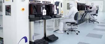
2 IMEC Established by state government of Flanders in Belgium Non-profit organization Initial investment: 62M Initial staff: ~ World-leading research in nanoelectronics Revenue: 275 M (incl. 44 M grant from Flanders government) Staff: >1750worldwide Worldwide collaboration >600 companies IMEC CAMPUS FAB 2 3,200 m 2 Clean Room 300 mm pilot line Ball Room, Clean sub-fab Continuous operation: 24hrs / 7 days FAB 1 4,800 m 2 Clean Room 1,750 m 2 Class mm pilot line Continuous operation: 24hrs / 7 days Total: 8,000 m 2 Clean Room 2


3 One of the world s most advanced state-of-the-art research facilities Fully operational since July 2006 (~ 500M ) IMEC IN THE WORLD imec the Netherlands imec office US imec Belgium imec China imec office Japan imec Taiwan Region IMEC the Netherlands: Research Organization in Eindhoven Part of Holst Centre 3
 TOTAL STAFF: >1775 INCL.")

4 IMEC S TOTAL REVENUE Total revenue (P&L), in million euro Grant from the Goverment of Flanders, in million euro ABOUT 60 REGIONS UNDER ONE ROOF foreign regions; 999 Belgian (January 2010) TOTAL STAFF: >1775 INCL. 521 RESIDENTS Belgians Albania Algeria Austria Brazil Bulgaria Canada Chili China Colombia Czechia Egypt Finland France Georgia Germany Great Britain Greece Guatemala Hungaria India Iran Iraq Ireland Israel Italy Ivory Coast Japan Korea Lithuania Malaysia Mexico Moldova Nepal Nicaragua Nigeria Pakistan Poland Portugal Romania Russia Serbia/Montenegro Singapore Slovakia South Africa Spain Sudan Sweden Switzerland Taiwan The Netherlands Tunisia Turkey U.S.A. Ukrainia Uzbekistan Venezuela Vietnam 4


5 RESEARCH CHALLENGE Need for research has never been as high Cost of research Continuous need for new materials and new processing techniques Total R&D cost vs. technology node, relative to 0.25mm, Source: TSMC PARTNERING FOR COST-EFFECTIVE RESEARCH Logic IC Memory IC Equipment Suppliers Universities Centralized Research Build critical Platform mass World-wide Share R&D Center of Excellence costs Material Suppliers Software suppliers Regional Government Europe 5


 STATE-OF-THE-ART 3D INTEGRATION APPLICATION AREAS")
6 BUSINESS LINES IMEC CORE CMOS Lithography Logic DRAM devices Interconnects IMEC CMORE SiGe MEMS Silicon photonics HUMAN++ Wearable and implantable body area networks (with Holst Centre) IMEC ENERGY Photovoltaics IMEC SMART SYSTEMS Power-efficient green radios Vision systems 3D integration Flash memories Vision systems Power devices and mixedsignal technologies Life sciences GN GaN power electronics and LEDs Large-area electronics and systems-in-foil (with Holst Centre) Emerging devices INSITE connecting technology and system design GaN power electronics and LEDs Wireless autonomous transducer solutions (with Holst Centre) STATE-OF-THE-ART 3D INTEGRATION APPLICATION AREAS DRIVING 3D INTEGRATION 6


7 APPLICATION AREAS DRIVING 3D INTEGRATION Mobile consumer Memory stacking High Performance computing Microsystem Integration MOBILE CONSUMER ELECTRONICS Modem 2G GSM/GPRS/EDGE 3G CDMA2000/EV-HDO HSPA/WCDMA 4G LTE Power Management RF Multimedia >30MP Camera Video encoding/decoding 2D/3D gaming Audio Low power >1 GHz/1V Quadcore CPU Memory 256gB NVM >8gb DRAM Low cost 7


8 3D FOR MOBILE CONSUMER APPLICATIONS Memory/logic IC stacks Increase memory bandwidth Maintaining low power ency (Mhz) Analog-logic stacks GB/s GDDR5 GDDR3 DDR3 LPDDR2 LPDDR1 Heterogeneous technology choices Time-to-market Reuse/Adapt device solutions in adjacent market segments telematics tracking IO frequ D stack IO count Low parallelism High parallelism Game smartbooks M2M routers Set-top box ebook HIGH DENSITY MEMORY STACKS Heterogeneous Memory Stack In use today: Wire-bonded die stack Not suitable for 3D- TSV die stacking Low speed & low I/O: today: Wire-bonded die stack Strongly cost driven Homogeneous Memory Stack High speed wide bandwidth & large # tiers 3D-TSV is enabling technology Repartitioned Memory stack & Logic and I/O circuits 3D-TSV is enabling technology Efficient use of scaled memory and scaled logic technologies 3D-TSV inside applications 8
 IO frequenc Thermal constraints limit memory on logic stacking Use")


9 HIGH PERFORMANCE APPLICATIONS Very High Memory bandwidth requirement Die stacking driver Very high power processor devices: y (Mhz) IO frequenc Thermal constraints limit memory on logic stacking Use of 3D SI Interposer substrates DRAM Mobile 12.8GB/s GDDR5 GDDR3 DDR3 LPDDR2 LP DDR1 Graphics 512GB/s 16XGDD R3x1Gb Mobile Wide IO IO count Logic DRAM Logic I/O MICROSYSTEM INTEGRATION Combining advanced logic and memory technologies with heterogeneous device technologies such as analog, sensor, actuator, MEMS,... e.g. 3D detector array systems: Sensor array Analog/Digital read-out array CMOS Digital Signal processing Often: Lower volume products Reuse of standard IC s Mainly : 3D TSV processing after device fabrication Use of Si-interposers ( MCM s ) 9
10 3D integration technology: BRIDGE BETWEEN MORE MOORE AND MORE THAN MOORE 3D INTEGRATION TECHNOLOGY: BRIDGE BETWEEN MORE MOORE AND MORE THAN MOORE Combining the benefits of scaling (density/performance) and alternate device technologies such as analog, high voltage, MEMS,... By optimization across technologies, cost effective solutions can be obtained 10


11 REQUIREMENTS FOR THE SUCCESS OF 3D INTEGRATION 3D Definitions, Roadmaps 3D-Design D tools & Design methodology for 3D 3D Technology 3D-Die stacking Packaging for 3D Yield 3D KGD for 3D 3D-Test strategies Supply Chain & Standardization IMEC 3D SYSTEM INTEGRATION PROGRAM Technology TSV technology Wafer thinning and backside processing D2W stacking technologies Packaging 3D-Die stacks Design Wafer Ø Cu TSV Ø Si Via height Cu Aspect ratio TSV min-pitch 3D system exploration Path finding IP for 3D integration : 3D memory, 3D-NOC Design for 3D integration Cost modeling Demonstration: design and fabrication 200 mm 5µm 25 µm 5:1 10 µm 3D-SIC 300 mm 5µm 50 µm 10:1 10 µm 130nm on 200 mm, 65nm to 22nm on 300 mm, CMOS 3D logic-on-logic, DRAM-on-logic, heterogeneous stacking 3D-WLP 200 mm 25 µm 50 µm 2:1 50 µm 11


12 IMEC 3D-SIC TSV TECHNOLOGY Key features : Realization of a Cu-nail after FEOL, before of BEOL High aspect ratio Cu damascene technique Single litho-step Current Cu-nail Ø = 5 µm, scaling down to 2 µm Aspect ratio s via Ø /depth studied: 1:5 and 1:10 5μm 25-26μm Si 10µm 3D INTEGRATION PROCESS FLOW IC fabrication line Wafer Thinning module Wafer edge conditioning Temporary bonding to a Si-Carrier wafer Wafer thinning Backside processing 3D-SIC via middle Si FEOL Cu nail Si FEOL Cu nail exposure & backside passivation 3D-WLP via last Standard device wafer Backside TSV process Backside redistribution layer & Cu or Cu/Sn µbump 3D-Stacking process Cu-Cu bonding or Cu/Sn µbump solder bonding 12


13 PROCESSES FOR THINNING AND HANDLING OF 3D TSV WAFERS Si (LSI) wafer Si carrier wafer Edge trim wafer Particle cleaning Temporary glue layer coating Wafer to Carrier bonding Wafer thinning by grinding Grinding damage removal (Wet/dry/CMP) and cleaning Thin wafer backside process 3D-SIC or 3D-WLP TSV process Wafer / carrier debonding clean & recycle carrier Dicing thin wafer on tape Particle clean 3D stacking Picture backside 3D-SIC TSV wafer after thinning and Si-recess etching 13
 High aspect ratio TSV (AR 2-3) Sn Kelvin TSV Resistance (mohm) Si Polymer 20 18 16 14 12 10 8 6 4 2 0 4-point Kelvin test structures 0")


14 3D-WLP, VIA LAST, BACKSIDE TSV TSVs using a polymer liner: Low Capacitance Thermal cycling 1000 cycles -40 C/150 C : no failures Low aspect ratio TSV (AR<1) High aspect ratio TSV (AR 2-3) Sn Kelvin TSV Resistance (mohm) Si Polymer point Kelvin test structures Sample number Kelvin TSV resistance (mohm) point Kelvin test structures Sample number 3D STACKING APPROACHES Die-to-wafer bonding approach: fast and accurate pickand-place step, followed by collective bonding. Cu/Sn µbump bonding: - Cu/Sn Transient-Liquid-Phase, TLP, (250 C) - diffusion bonding (150 C) - Pitch Scaling : µm - Bump planarisation Cu/Cu bonding : - High T Thermo-compression bonding - Low T Cu/Cu insertion bonding Cu oxide removal & prevention No-flow & wafer-level, pre-applied underfill 14


15 HYBRID D2W BONDING: Fast D2W placement + WL collective bonding BEOL BEOL BEOL Si Cu pad BEOL Cu nail polymer Si Cu pad BEOL Cu nail polymer Si Cu pad BEOL Cu nail polymer Si Si Si Cu nail No polymer polymer landing pad Polymer Dot Pattern 15


 10 0 0 100 200 300 RO Delay")
16 3D-130C stacked circuit demonstration IMEC 130nm CMOS 2 metal layers platform technology 3D-SIC TSV: Ø 5µm, AR 5:1 D2W collective Cu/Cu bonding Pads 12 on top layer 7 on bottom layer TOP BOTTO M 3D NOC test circuit: Two layer stack using 100 TSVs Memory Traffic Generator Switch Switch Via Control/Readout TSV bundle 36 x 2 NoC 4 x JTAG 1 x 3 plane ID 2 x 6 VDD/GND = 100 vias 10um Top tier Top tier Bottom tier 5um 25um Cu-Cu bonding Cu-Cu bonding RO Power [µw/stage] TSV R ~20mΩ; C ~40fF (depletion) TSV leakage << 1nA TSV Breakdown voltage > 100V Cascaded 3D ROs: measurements confirm values of TSV R and C 60 2D RO 41_ref 50 2D RO 21_ref 40 3D RO 41 TSV 30 3D RO 21 TSV Symbols: measured 20 lines: simulation (Spectre) RO Delay [ps/stage] 16


17 CONCLUSIONS 3D-System integration technologies are well suited to realize high integration density and high performance heterogeneous systems. System-level requirements define the required 3D integration technology Main 3D-TSV technology areas: 3D-SIC, via middle TSV, for highest density 3D-stacking 3D-WLP, via last TSV, for post-fab TSV s for microsystem integration Silicon interposers with TSV connections for high performance applications 3D-Integration technology has three key components: TSV technology Wafer thinning and thin wafer handling technology Micro-bump interconnect technology for 3D stacking 17
Global pay TV revenues crawl to $200 billion
 Global pay TV revenues crawl to $200 billion Based on forecasts for 80 countries, pay TV revenues will climb to US$200 billion in 2017, up by US$23 billion on 2011 but up by only US$2 billion (1%) on 2016,
BFI RESEARCH AND STATISTICS PUBLISHED AUGUST 2016 THE UK FILM MARKET AS A WHOLE. Image: Mr Holmes courtesy of eone Films
 BFI RESEARCH AND STATISTICS PUBLISHED AUGUST 2016 THE UK FILM MARKET AS A WHOLE Image: Mr Holmes courtesy of eone Films THE UK FILM MARKET AS A WHOLE The UK is the third largest film market in the world,
Wafer Thinning and Thru-Silicon Vias
 Wafer Thinning and Thru-Silicon Vias The Path to Wafer Level Packaging jreche@trusi.com Summary A new dry etching technology Atmospheric Downstream Plasma (ADP) Etch Applications to Packaging Wafer Thinning
Installation Instructions. What This Option Provides
 Installation Instructions IN Bulletin 1336 PLUS, 1336 IMPACT, and 1336 FORCE TM NEMA Type 4/12 Gasket Kit Installation & Drive Mounting (Catalog Number 1336 RF2 1336S RF3 1336 RF4 1336 RF5 1336 RF6 1336
Through Silicon Via Testing Known Good Die (KGD) or Probably Good Die (PGD) Doug Lefever Advantest
 or Probably Good Die (PGD) Doug Lefever Advantest") Through Silicon Via Testing Known Good Die (KGD) or Probably Good Die (PGD) Doug Lefever Advantest Single Die Fab Yield will drive Cost Equation. Yield of the device to be stacked 100% 90% 80% Yield of
Through Silicon Via Testing Known Good Die (KGD) or Probably Good Die (PGD) Doug Lefever Advantest Single Die Fab Yield will drive Cost Equation. Yield of the device to be stacked 100% 90% 80% Yield of
InvenSense Fabless Model for the MEMS Industry
 InvenSense Fabless Model for the MEMS Industry HKSTP Symposium Aug 2016 InvenSense, Inc. Proprietary Outline MEMS Market InvenSense CMOS-MEMS Integration InvenSense Shuttle Program and Process MEMS MARKET
SEMICONDUCTOR TECHNOLOGY -CMOS-
 SEMICONDUCTOR TECHNOLOGY -CMOS- Fire Tom Wada What is semiconductor and LSIs Huge number of transistors can be integrated in a small Si chip. The size of the chip is roughly the size of nails. Currently,
SEMICONDUCTOR TECHNOLOGY -CMOS-
 SEMICONDUCTOR TECHNOLOGY -CMOS- Fire Tom Wada 2011/12/19 1 What is semiconductor and LSIs Huge number of transistors can be integrated in a small Si chip. The size of the chip is roughly the size of nails.
Advanced WLP Platform for High-Performance MEMS. Presented by Dean Spicer, Director of Engineering
 Advanced WLP Platform for High-Performance MEMS Presented by Dean Spicer, Director of Engineering 1 May 11 th, 2016 1 Outline 1. Application Drivers for High Performance MEMS Sensors 2. Approaches to Achieving
9 rue Alfred Kastler - BP Nantes Cedex 3 - France Phone : +33 (0) website :
 website :") 9 rue Alfred Kastler - BP 10748-44307 Nantes Cedex 3 - France Phone : +33 (0) 240 180 916 - email : info@systemplus.fr - website : www.systemplus.fr January 2012 Written by: Maher SAHMIMI DISCLAIMER :
9 rue Alfred Kastler - BP 10748-44307 Nantes Cedex 3 - France Phone : +33 (0) 240 180 916 - email : info@systemplus.fr - website : www.systemplus.fr January 2012 Written by: Maher SAHMIMI DISCLAIMER :
Verification of HBM through Direct Probing on MicroBumps
 Verification of HBM through Direct Probing on MicroBumps FormFactor Sung Wook Moon SK hynix Outline HBM market HBM test flow Device structure overview Key test challenges addressed Signal delivery and
Supplemental Information. Form and Function in Human Song. Samuel A. Mehr, Manvir Singh, Hunter York, Luke Glowacki, and Max M.
 Current Biology, Volume 28 Supplemental Information Form and Function in Human Song Samuel A. Mehr, Manvir Singh, Hunter York, Luke Glowacki, and Max M. Krasnow 1.00 1 2 2 250 3 Human Development Index
Transforming Electronic Interconnect Breaking through historical boundaries Tim Olson Founder & CTO
 Transforming Electronic Interconnect Breaking through historical boundaries Tim Olson Founder & CTO Remember when? There were three distinct industries Wafer Foundries SATS EMS Semiconductor Devices Nanometers
Applied Materials. 200mm Tools & Process Capabilities For Next Generation MEMS. Dr Michel (Mike) Rosa
 Rosa") Applied Materials 200mm Tools & Process Capabilities For Next Generation MEMS Dr Michel (Mike) Rosa 200mm MEMS Global Product / Marketing Manager, Components and Systems Group (CSG), Applied Global Services
Applied Materials 200mm Tools & Process Capabilities For Next Generation MEMS Dr Michel (Mike) Rosa 200mm MEMS Global Product / Marketing Manager, Components and Systems Group (CSG), Applied Global Services
Sharif University of Technology. SoC: Introduction
 SoC Design Lecture 1: Introduction Shaahin Hessabi Department of Computer Engineering System-on-Chip System: a set of related parts that act as a whole to achieve a given goal. A system is a set of interacting
Future trends for SiP In Medical Implant Applications
 Future trends for SiP In Medical Implant Applications Piers Tremlett, Zarlink Semiconductor NMI at TWI, 12 Dec 07 A case study This presentation uses Zarlink s Medical RF device To consider potential embedded
Debugging Memory Interfaces using Visual Trigger on Tektronix Oscilloscopes
 Debugging Memory Interfaces using Visual Trigger on Tektronix Oscilloscopes Application Note What you will learn: This document focuses on how Visual Triggering, Pinpoint Triggering, and Advanced Search
REPORT ON THE STATUS OF CONTRIBUTIONS TO THE CORE BUDGET FOR THE BIENNIUM Note by the secretariat
 UNITED NATIONS Distr. GENERAL FCCC/CP/1997/INF.4 25 November 1997 ENGLISH ONLY CONFERENCE OF THE PARTIES Third session Kyoto, 1-10 December 1997 REPORT ON THE STATUS OF CONTRIBUTIONS TO THE CORE BUDGET
Arc-fault Protection System
 Short Form Catalogue Arc-fault Protection System Protection of Switchboards Improve personnel safety. Minimize production down time. Reduce damage to material and the cost of repair or replacement. Arcing
Tektronix Logic Analyzer Probes P6900 Series Datasheet for DDR Memory Applications
 Tektronix Logic Analyzer Probes P6900 Series Datasheet for DDR Memory Applications Leading probe solutions for real-time digital systems analysis Verification and debug of today's high speed, low voltage
Flexible Electronics Production Deployment on FPD Standards: Plastic Displays & Integrated Circuits. Stanislav Loboda R&D engineer
 Flexible Electronics Production Deployment on FPD Standards: Plastic Displays & Integrated Circuits Stanislav Loboda R&D engineer The world-first small-volume contract manufacturing for plastic TFT-arrays
Obsolete Product(s) - Obsolete Product(s)
 - Obsolete Product(s)") IPAD TM 3 LINES EMI FILTER AND ESD PROTECTION MAIN PRODUCT APPLICATIONS EMI filtering and ESD protection for : SIM Interface (Subscriber Identify Module) UIM Interface (Universal Identify Module) DESCRIPTION
IPAD TM 3 LINES EMI FILTER AND ESD PROTECTION MAIN PRODUCT APPLICATIONS EMI filtering and ESD protection for : SIM Interface (Subscriber Identify Module) UIM Interface (Universal Identify Module) DESCRIPTION
EMIF QCF 4 LINE LOW CAPACITANCE EMI FILTER AND ESD PROTECTION IPAD
 IPAD EMIF04-1502QCF 4 LINE LOW CAPACITANCE EMI FILTER AND ESD PROTECTION MAIN PRODUCT CHARACTERISTICS: Where EMI filtering in ESD sensitive equipment is required : LCD and camera for Mobile phones Computers
RFSOI and FDSOI enabling smarter and IoT applications. Kirk Ouellette Digital Products Group STMicroelectronics
 RFSOI and FDSOI enabling smarter and IoT applications Kirk Ouellette Digital Products Group STMicroelectronics ST in the IoT already Today 2 Kirk Ouellette More then Moore Workshop - Shanghai - March 17,
Advanced Sensor Technologies
 Advanced Sensor Technologies Jörg Amelung Fraunhofer Institute for Photonics Microsystems Name of presenter date Sensors as core element for IoT Next phase of market grow New/Advanced Requirements based
Video Reference Timing with Tektronix Signal Generators
 Using Stay GenLock Video Reference Timing with Tektronix Signal Generators Technical Brief Digital video systems require synchronization and test signal sources with low jitter and high stability. The
40 Gb/s PatternPro Programmable Pattern Generator PPG4001 Datasheet
 40 Gb/s PatternPro Programmable Pattern Generator PPG4001 Datasheet Applications Semiconductor device testing Optical component testing Transceiver module testing The Tektronix PPG4001 PatternPro programmable
CMP and Current Trends Related to Advanced Packaging
 CMP and Current Trends Related to Advanced Packaging Robert L. Rhoades, Ph.D. NCCAVS TFUG-CMPUG Joint Meeting June 7, 2017 Semiconductor Equipment Spare Parts and Service CMP Foundry Foundry Click to edit
DEPFET Active Pixel Sensors for the ILC
 DEPFET Active Pixel Sensors for the ILC Laci Andricek for the DEPFET Collaboration (www.depfet.org) The DEPFET ILC VTX Project steering chips Switcher thinning technology Simulation sensor development
More light, less power comsumption. Living with
 More light, less power comsumption Living with LED-Lights and Energy Saving Lamps by Energy Saving Lamps The electricity costs rise and rise... Scotch the power companies! CAMELION energy saving lamps
AIXTRON in EXCILIGHT project
 AIXTRON SE AIXTRON in EXCILIGHT project Gintautas Simkus ABOUT AIXTRON 2 Who we are Headquarter based in Herzogenrath, Germany Worldwide presence with 14 sales/representatives offices and production facilities
EMIF02-SPK01F2 2 LINE EMI FILTER AND ESD PROTECTION Low-pass Filter Input Output Ri/o = 10 Ω Cline = 200 pf GND GND GND
 IPAD EMIF02-SPK01F2 2 LINE EMI FILTER AND ESD PROTECTION MAIN PRODUCT CHARACTERISTICS: Where EMI filtering in ESD sensitive equipment is required : Mobile phones and communication systems Computers, printers
Advanced MEMS Packaging
 Advanced MEMS Packaging John H. Lau Chengkuo Lee C. S. Premachandran Yu Aibin Ш New York Chicago San Francisco Lisbon London Madrid Mexico City Milan New Delhi San Juan Seoul Singapore Sydney Toronto Contents
The Great Transition: Shifting from Fossil Fuels to Solar and Wind Energy Supporting Data - Climate
 The Great Transition: Shifting from Fossil Fuels to Solar and Wind Energy Supporting Data - Climate Carbon Emissions Global Carbon Dioxide Emissions from Fossil Fuel Burning, 1751-2013 GRAPH: Global Carbon
Troubleshooting Analog to Digital Converter Offset using a Mixed Signal Oscilloscope APPLICATION NOTE
 Troubleshooting Analog to Digital Converter Offset using a Mixed Signal Oscilloscope Introduction In a traditional acquisition system, an analog signal input goes through some form of signal conditioning
Selection Results for the STEP traineeships published on the 9th of April, 2018
 Selection Results for the STEP traineeships published on the 9th of April, 2018 Please, have in mind: - The selection results are at the moment incomplete. We are still waiting for the feedback from several
Leveraging 300 mm Technology Solutions to Enable New MEMS Process Capabilities
 Leveraging 300 mm Technology Solutions to Enable New MEMS Process Capabilities Evan Patton Semicon Europa November 2017 Lam Research Corp. 1 Presentation Outline The Internet of Things (IoT) as a market
HCF4054B 4 SEGMENT LIQUID CRYSTAL DISPLAY DRIVER WITH STROBED LATCH FUNCTION
 4 SEGMENT LIQUID CRYSTAL DISPLAY DRIVER WITH STROBED LATCH FUNCTION QUIESCENT CURRENT SPECIF. UP TO 20V OPERATION OF LIQUID CRYSTALS WITH CMOS CIRCUITS PROVIDES ULTRA LOW POWER DISPLAYS EQUIVALENT AC OUTPUT
THE BEAUTY OF THE INFLATABLE SCREEN
 THE BEAUTY OF THE INFLATABLE SCREEN AIRSCREEN 100ft x 60ft (30m x 18m) Brussels, Belgium Drive-in cinema » AIRSCREEN remains the world s «leader in giant inflatable screens. Technology InAVation Awards
Spring Probes and Probe Cards for Wafer-Level Test. Jim Brandes Multitest. A Comparison of Probe Solutions for an RF WLCSP Product
 Session 6 AND, AT THE WAFER LEVEL For many in the industry, performing final test at the wafer level is still a novel idea. While providing some much needed solutions, it also comes with its own set of
Agilent M9362A-D01-F26 PXIe Quad Downconverter
 Agilent M9362A-D01-F26 PXIe Quad Downconverter 10 MHz to 26.5 GHz Data Sheet Challenge the Boundaries of Test Agilent Modular Products OVERVIEW Introduction The Agilent M9362A-D01-F26 is a PXIe 3-slot,
NEW. Cable/Pipe sizes. InsertStrip. MainBlock
 W E N HandiBlock Newly developed insert block that provides greater flexibility, simple and safe installation. Tested and approved by leading classification societies and patented world wide. NEW Greater
46 GBaud Multi-Format Optical Transmitter
 46 GBaud Multi-Format Optical Transmitter OM5110 Datasheet Applications Testing coherent optical receivers Golden reference coherent optical transmitter Transmitter for multi-carrier superchannel systems
Arc Detecting and Protection System
 Data Sheet Arc Detecting and Protection System Protection of Switchboards Personnel safety, the cost of employees. Loss of supply and operation of the switchboard, the cost of a production down time. Damage
3D-CHIP TECHNOLOGY AND APPLICATIONS OF MINIATURIZATION
 3D-CHIP TECHNOLOGY AND APPLICATIONS OF MINIATURIZATION 23.08.2018 I DAVID ARUTINOV CONTENT INTRODUCTION TRENDS AND ISSUES OF MODERN IC s 3D INTEGRATION TECHNOLOGY CURRENT STATE OF 3D INTEGRATION SUMMARY
MEMS Technologies Dresden - Product Development and Fabrication at IPMS Dresden
 MEMS Technologies Dresden - Product Development and Fabrication at IPMS Dresden MEMS Technologies Dresden - Product Development and Fabrication at IPMS Dresden Michael Müller, Matthias List Outline FhG-IPMS
High Performance Microprocessor Design and Automation: Overview, Challenges and Opportunities IBM Corporation
 High Performance Microprocessor Design and Automation: Overview, Challenges and Opportunities Introduction About Myself What to expect out of this lecture Understand the current trend in the IC Design
THE BEAUTY OF THE INFLATABLE SCREEN
 THE BEAUTY OF THE INFLATABLE SCREEN AIRSCREEN 100ft x 60ft (30m x 18m) Brussels, Belgium Drive-in cinema » AIRSCREEN remains the world s «leader in giant inflatable screens. Technology InAVation Awards
Keysight Technologies Multi-Channel Audio Test using the Keysight U8903A Audio Analyzer
 Keysight Technologies Multi-Channel Audio Test using the Keysight U8903A Audio Analyzer Power supply For Instrument Control PC for post-analysis DUT Switch for channels expansion Audio analyzer (2 channels)
TA0311 TECHNICAL ARTICLE High Temperature Electronics 1 Introduction 2 Why the need for high-temperature semiconductors?
 TECHNICAL ARTICLE High Temperature Electronics 1 Introduction In the semiconductor world, there are numerous products specified with an industrial temperature range (-40/+85 C), and somewhat fewer with
Video Quality Monitors Sentry Edge II Datasheet
 Video Quality Monitors Sentry Edge II Datasheet Remote management of RF measurement collection Proactively detect RF issues before they impact subscribers Full range of Transport Stream monitoring capabilities
UV Nanoimprint Tool and Process Technology. S.V. Sreenivasan December 13 th, 2007
 UV Nanoimprint Tool and Process Technology S.V. Sreenivasan December 13 th, 2007 Agenda Introduction Need tool and process technology that can address: Patterning and CD control Alignment and Overlay Defect
Keysight N9355/6 Power Limiters 0.01 to 18, 26.5 and 50 GHz High Performance Power Limiters. Technical Overview
 Keysight N9355/6 Power Limiters 0.01 to 18, 26.5 and 50 GHz High Performance Power Limiters Technical Overview Introduction Broad frequency range up to 50 GHz maximizes the operating range of your instrument
VT5365. Single-chip optical mouse sensor for wireless applications. Features. Applications. Technical specifications. Description.
 Single-chip optical mouse sensor for wireless applications Data Brief Features One chip solution with internal micro and minimal external circuitry 1.8V (single battery) or 2.0 V to 3.2 V (serial batteries)
The FOOTBALL Sponsoring Qualifiers for EURO June. 2010, Ulrike Schmid/Peter Rossegg
 The FOOTBALL Sponsoring Qualifiers for EURO 2012 June. 2010, Ulrike Schmid/Peter Rossegg The Groups and Group A Group B Group C Group D 1 Germany 1 Russia 1 Italy 1 France 2 Turkey 2 Slovakia 2 Serbia
BAL-NRF01D3. 50 ohm balun transformer for 2G45 ISM matched Nordic s chipset: nrf24le1 QFN32, nrf24ap2-1ch and nrf24ap2-8ch. Features.
 50 ohm balun transformer for 2G45 ISM matched Nordic s chipset: nrf24le1 QFN32, nrf24ap2-1ch and nrf24ap2-8ch Features 50 nominal input / conjugate match to nrf24le1 QFN32, nrf24ap2-1ch and nrf24ap2-8ch
IEEE TRANSACTIONS ON VERY LARGE SCALE INTEGRATION (VLSI) SYSTEMS, VOL. 23, NO. 2, FEBRUARY
 SYSTEMS, VOL. 23, NO. 2, FEBRUARY") IEEE TRANSACTIONS ON VERY LARGE SCALE INTEGRATION (VLSI) SYSTEMS, VOL. 23, NO. 2, FEBRUARY 2015 317 Scan Test of Die Logic in 3-D ICs Using TSV Probing Brandon Noia, Shreepad Panth, Krishnendu Chakrabarty,
IEEE TRANSACTIONS ON VERY LARGE SCALE INTEGRATION (VLSI) SYSTEMS, VOL. 23, NO. 2, FEBRUARY 2015 317 Scan Test of Die Logic in 3-D ICs Using TSV Probing Brandon Noia, Shreepad Panth, Krishnendu Chakrabarty,
I-fuse TM : Best OTP for FD-SOI and Sub-14nm
 I-fuse TM : Best OTP for FD-SOI and Sub-14nm Shine Chung, Chairman May, 2017 Attopsemi Technology 1A2-A1 No. 1 Li-Hsin 1st Rd, Hsinchu, Taiwan 300-76 (886) 3-666-3150x211, (886) 920-566-218 1 1 About Attopsemi
Agilent Understanding the Agilent 34405A DMM Operation Application Note
 Agilent Understanding the Agilent 34405A DMM Operation Application Note Introduction Digital multimeter (DMM) is a basic device in the electrical world and its functions are usually not fully utilized.
Coverage analysis of publications of University of Mysore in Scopus
 International Journal of Research in Library Science ISSN: 2455-104X ISI Impact Factor: 3.723 Indexed in: IIJIF, ijindex, SJIF,ISI, COSMOS Volume 2,Issue 2 (July-December) 2016,91-97 Received: 19 Aug.2016
40 Gb/s PatternPro Programmable Pattern Generator PPG4001 Datasheet
 40 Gb/s PatternPro Programmable Pattern Generator PPG4001 Datasheet The Tektronix PPG4001 PatternPro programmable pattern generator provides stressed pattern generation for high-speed Datacom testing.
EMIF C2 IPAD. 6 line EMI filter and ESD protection. Main product characteristics. Description. Order Code. Benefits
 IPAD 6 line EMI filter and ESD protection Main product characteristics Where EMI filtering in ESD sensitive equipment is required: Mobile phones and communication systems Computers, printers and MCU Boards
nmos transistor Basics of VLSI Design and Test Solution: CMOS pmos transistor CMOS Inverter First-Order DC Analysis CMOS Inverter: Transient Response
 nmos transistor asics of VLSI Design and Test If the gate is high, the switch is on If the gate is low, the switch is off Mohammad Tehranipoor Drain ECE495/695: Introduction to Hardware Security & Trust
Multi Content Market Japan Content Showcase Features of Japan Content Showcase JCS. Online Library. TIMM & Showcase Live TIMM & Free Service
 Multi Content Market Japan Content Showcase 2017 "Japan Content Showcase 2017", a multi content market featuring TV, films, music, and animation, will be held as a joint market of the following: TIMM Tokyo
24. Scaling, Economics, SOI Technology
 24. Scaling, Economics, SOI Technology Jacob Abraham Department of Electrical and Computer Engineering The University of Texas at Austin VLSI Design Fall 2017 December 4, 2017 ECE Department, University
Nano-Imprint Lithography Infrastructure: Imprint Templates
 Nano-Imprint Lithography Infrastructure: Imprint Templates John Maltabes Photronics, Inc Austin, TX 1 Questions to keep in mind Imprint template manufacturability Resolution Can you get sub30nm images?
Low Temperature/Low Load Damage Free Flip Chip Technology for NEMS/MEMS, IC and IoT Applications. CONNECTEC JAPAN Corporation CEO Katsunori, Hirata
 Low Temperature/Low Load Damage Free Flip Chip Technology for NEMS/MEMS, IC and IoT Applications CONNECTEC JAPAN Corporation CEO Katsunori, Hirata CONNECTEC JAPAN Corporation Company Profile Company Name
Automatic License Plate Recognition. 7.0 User Guide
 Automatic License Plate Recognition 7.0 User Guide Contents Contents Introduction...3 Camera field of view...3 Camera frame rate...3 Installation... 5 Requirements... 5 Install Automatic License Plate
Adesto Acquires S3 Semiconductors
 Beyond Memories Adesto Acquires S3 Semiconductors May 9, 2018 A Brilliant Combination 3600 Peterson Way Santa Clara, California 95054 www.adestotech.com Who is Adesto Technologies? Inventing Application-Specific,
In the September/October issue of Small Times
 Thinking outside the chip: MEMS-based systems solutions by Roger H. Grace, Roger Grace Associates In the September/October issue of Small Times (p.32) I introduced a MEMS Commercialization Report Card
UK Television Exports FY 2013/2014
 UK Television Exports FY 2013/2014 Page 1 of 5 The annual UK Television Exports Survey highlights the popularity of UK programming abroad by collecting revenue figures relating to the international activity
SoC IC Basics. COE838: Systems on Chip Design
 SoC IC Basics COE838: Systems on Chip Design http://www.ee.ryerson.ca/~courses/coe838/ Dr. Gul N. Khan http://www.ee.ryerson.ca/~gnkhan Electrical and Computer Engineering Ryerson University Overview SoC
The Alice Silicon Pixel Detector (SPD) Peter Chochula for the Alice Pixel Collaboration
 Peter Chochula for the Alice Pixel Collaboration") The Alice Silicon Pixel Detector (SPD) Peter Chochula for the Alice Pixel Collaboration The Alice Pixel Detector R 1 =3.9 cm R 2 =7.6 cm Main Physics Goal Heavy Flavour Physics D 0 K π+ 15 days Pb-Pb data
The Alice Silicon Pixel Detector (SPD) Peter Chochula for the Alice Pixel Collaboration The Alice Pixel Detector R 1 =3.9 cm R 2 =7.6 cm Main Physics Goal Heavy Flavour Physics D 0 K π+ 15 days Pb-Pb data
Layers of Innovation: How Signal Chain Innovations are Creating Analog Opportunities in a Digital World
 The World Leader in High Performance Signal Processing Solutions Layers of Innovation: How Signal Chain Innovations are Creating Analog Opportunities in a Digital World Dave Robertson-- VP of Analog Technology
Broadcasting ANTENNAS Elements & Systems Coverage Studies
 Broadcasting ANTENNAS Elements & Systems Coverage Studies 2 BROADCASTING ANTENNAS Elements & Systems Coverage Studies COEL brand Digital, Mobile and Analog Broadcasting services Frequency bands: VHF I,
DFT. Rotating Vane Flow Meter, Counter, Doser. for liquids l/min. Measuring accuracy: 2.5% f. s. : 16 bar; t max
 Rotating Vane Flow Meter, Counter, Doser for liquids measuring monitoring analysing DFT OMeasuring O range: 0.2-2.0... 3-60 l/min OO Measuring accuracy: 2.5% f. s. OO p max : 16 bar; t max : 80 C OProcess
EECS150 - Digital Design Lecture 2 - CMOS
 EECS150 - Digital Design Lecture 2 - CMOS January 23, 2003 John Wawrzynek Spring 2003 EECS150 - Lec02-CMOS Page 1 Outline Overview of Physical Implementations CMOS devices Announcements/Break CMOS transistor
DFT. Compact Paddle Flow Sensor
 Compact Paddle Flow Sensor measuring monitoring analyzing DFT Measuring Ranges: 0.05...0.50 to 0.8...15 GPM PTFE or Brass Bodies Pulse Output Standard Optional Analog Outputs, Digital Displays, Totalizer
PatternPro Error Detector PED3200 and PED4000 Series Datasheet
 PatternPro Error Detector PED3200 and PED4000 Series Datasheet Auto-synchronization to input pattern The PED3200 and PED4000 series programmable error detectors offer effective multi-channel BER for stressed
MPEG Solutions. Transition to H.264 Video. Equipment Under Test. Test Domain. Multiplexer. TX/RTX or TS Player TSCA
 MPEG Solutions essed Encoder Multiplexer Transmission Medium: Terrestrial, Satellite, Cable or IP TX/RTX or TS Player Equipment Under Test Test Domain TSCA TS Multiplexer Transition to H.264 Video Introduction/Overview
Keysight Technologies Understanding and Improving Network Analyzer Dynamic Range. Application Note
 Keysight Technologies Understanding and Improving Network Analyzer Dynamic Range Application Note Introduction Achieving the highest possible network analyzer dynamic range is extremely important when
Scalable self-aligned active matrix IGZO TFT backplane technology and its use in flexible semi-transparent image sensors. Albert van Breemen
 Scalable self-aligned active matrix IGZO TFT backplane technology and its use in flexible semi-transparent image sensors Albert van Breemen Image sensors today 1 Dominated by silicon based technology on
Identifying Setup and Hold Violations with a Mixed Signal Oscilloscope APPLICATION NOTE
 Identifying Setup and Hold Violations with a Mixed Signal Oscilloscope Introduction Timing relationships between signals are critical to reliable operation of digital designs. With synchronous designs,
Description. Table 1. Device summary. Order codes Temperature range [ C] Package Packing. LPS2HBTR -30 to +105 HLGA - 10L
![Description. Table 1. Device summary. Order codes Temperature range [ C] Package Packing. LPS2HBTR -30 to +105 HLGA - 10L](/thumbs/81/84215301.jpg "Description. Table 1. Device summary. Order codes Temperature range [ C] Package Packing. LPS2HBTR -30 to +105 HLGA - 10L") MEMS pressure sensor: 260-1260 hpa absolute digital output barometer Applications Data brief Altimeter and barometer for portable devices GPS applications Weather station equipment Indoor navigation (Altitude
MEMS pressure sensor: 260-1260 hpa absolute digital output barometer Applications Data brief Altimeter and barometer for portable devices GPS applications Weather station equipment Indoor navigation (Altitude
DesignEmotionAtmosphere
 DesignEmotionAtmosphere Man s mind once stretched by a new idea, never regains its original dimension. Modern consumers are not only looking for recognition. They want to experience things, be stimulated
Keysight E4729A SystemVue Consulting Services
 Keysight E4729A SystemVue Consulting Services DOCSIS 3.1 Baseband Verification Library SystemVue Algorithm Reference Library for Data-Over-Cable Service Interface Specifications (DOCSIS 3.1), Intended
TKK S ASIC-PIIRIEN SUUNNITTELU
 Design TKK S-88.134 ASIC-PIIRIEN SUUNNITTELU Design Flow 3.2.2005 RTL Design 10.2.2005 Implementation 7.4.2005 Contents 1. Terminology 2. RTL to Parts flow 3. Logic synthesis 4. Static Timing Analysis
Low Cost, High Speed Spectrum Analyzers For RF Manufacturing APPLICATION NOTE
 Low Cost, High Speed Spectrum Analyzers For RF Manufacturing APPLICATION NOTE Application Note Table of Contents Spectrum Analyzers in Manufacturing...3 Low Cost USB Spectrum Analyzers for Manufacturing...3
High Power ARNS/IFF Limiter Module: Ultra Low Flat Leakage & Fast Recovery Time
 RELEASED RFLM-961122MC-299 High Power ARNS/IFF Limiter Module: Ultra Low Flat Leakage & Fast Recovery Time Features: SMT Limiter Module: 8mm x 5mm x 2.5mm Frequency Range: 960 MHz to 1,215 MHz High Average
Bluetooth. Wireless Technology Solutions. STMicroelectronics More Intelligent Solutions
 Bluetooth Wireless Technology Solutions STMicroelectronics More Intelligent Solutions ST Strategy ST s offer of the underlying Wireless Technology begins first with the silicon process technology offering.
L CHANNEL LOW POWER PREAMPLIFIER
 1 FEATURES Dual Power Supplies of +5V, 10% and -3v, 6% Low Power consumption; 980 mw @ 800Mb/s (Single Head 100% Write mode duty cycle, Random pattern, Iw = 40mA, Max Ovs). Flip Chip package.l6316 Differential
Keysight Technologies Millimeter Wave Frequency Extenders From Virginia Diodes Inc. for the Keysight X-Series Signal Analyzers. Technical Overview
 Keysight Technologies Millimeter Wave Frequency Extenders From Virginia Diodes Inc. for the Keysight X-Series Signal Analyzers Technical Overview The Keysight Technologies, Inc. X-series signal analyzers
HCF40193B PRESETTABLE UP/DOWN COUNTERS (DUAL CLOCK WITH RESET) BINARY TYPE
 BINARY TYPE") PRESETTABLE UP/DOWN COUNTERS (DUAL CLOCK WITH RESET) BINARY TYPE INDIVIDUAL CLOCK LINES FOR COUNTING UP OR COUNTING DOWN SYNCHRONOUS HIGH-SPEED CARRY AND BORROW PROPAGATION DELAYS FOR CASCADING ASYNCHRONOUS
PRESETTABLE UP/DOWN COUNTERS (DUAL CLOCK WITH RESET) BINARY TYPE INDIVIDUAL CLOCK LINES FOR COUNTING UP OR COUNTING DOWN SYNCHRONOUS HIGH-SPEED CARRY AND BORROW PROPAGATION DELAYS FOR CASCADING ASYNCHRONOUS
Title: STMicroelectronics NIR Camera Sensor Pages: 97 Date: December 2017 Format: PDF & Excel file Price: Full report: EUR 3,490
 STMicroelectronics Near Infrared Camera Sensor in the Apple iphone X The first NIR camera sensor with multiple innovations based on imager-silicon-oninsulator substrate from SOITEC, supplied and produced
Self-Aligned Double Patterning for 3xnm Flash Production
 Self-Aligned Double Patterning for 3xnm Flash Production Chris Ngai Dir of Process Engineering & Lithography Maydan Technology Center Group Applied Materials, Inc. July 16 th, 2008 Overview Double Patterning
247E4.
 247E4 www.philips.com/welcome 1......... 5...5...7 Definition Link)... 38............ 11......... 20...... 21... 26 27 33...... 4 247E4 2 1 5 MHL-HDMI or HDMI MHL HDMI 3 2 MHL-HDMI or HDMI HDMI 1 3
Fixed Optical Filter Portfolio for the Cisco ONS Multiservice Transport Platform
 Data Sheet Fixed Optical Filter Portfolio for the Cisco ONS 15454 Multiservice Transport Platform The Cisco ONS 15454 Multiservice Transport Platform (MSTP) provides a comprehensive, intelligent dense
21 rue La Noue Bras de Fer Nantes - France Phone : +33 (0) website :
 website :") 21 rue La Noue Bras de Fer - 44200 Nantes - France Phone : +33 (0) 240 180 916 - email : info@systemplus.fr - website : www.systemplus.fr 2012 September - Version 1 Written by: Maher Sahmimi DISCLAIMER
21 rue La Noue Bras de Fer - 44200 Nantes - France Phone : +33 (0) 240 180 916 - email : info@systemplus.fr - website : www.systemplus.fr 2012 September - Version 1 Written by: Maher Sahmimi DISCLAIMER
Keysight N9355/6 Power Limiters 0.01 to 18, 26.5 and 50 GHz High Performance Power Limiters. Technical Overview
 Keysight N9355/6 Power Limiters 0.01 to 18, 26.5 and 50 GHz High Performance Power Limiters Technical Overview Introduction Broad frequency range up to 50 GHz maximizes the operating range of your instrument