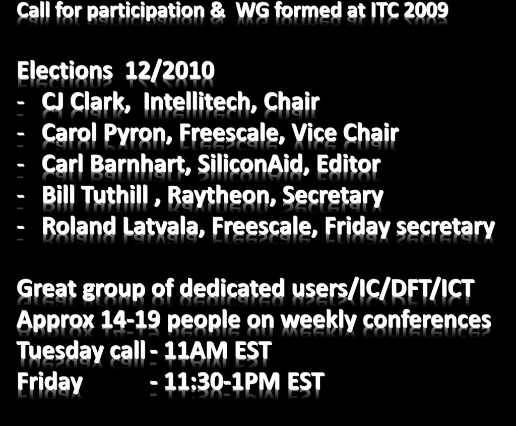
1
|
|
|
- Marjorie McCarthy
- 5 years ago
- Views:
Transcription


1 1
2 2
3 3

4 BOUNDARY REGISTER INIT-DATA REGISTER 0 1 ADC DAC System Reset SysReset On-chip Reset via TAP PLL Protocol Swing ECID Unique ID 0 1 AC/DC Voltage Monitor PRBS CMMV PCB Level Obstacle User Defined Chain(s) Logic BIST Memory BIST BIST Failure Data For ATE PCB Level Obstacle IC1 IR & Decode & Muxing TAP 4
5 5


6 settdi u1.mbist-csr start settdi u1.alg walk1 drscan runtest set result [gettdo status] If {$result!= pass} puts memorybist failed 6
7 7
8 8


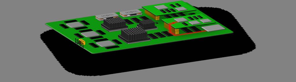
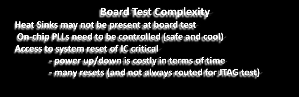
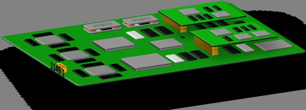
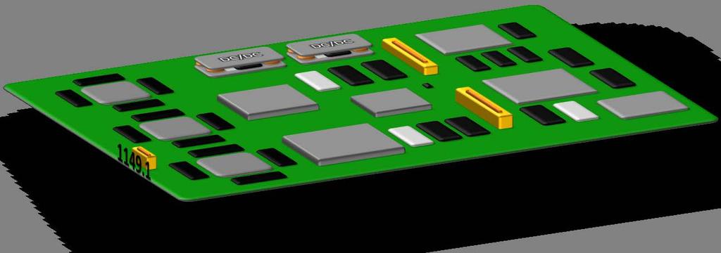
9 Stable temperature Changing temp 50ohm Z T DUT card design, dedicated Std. FR4, multi-ic signals Low noise Power, DC/DC converters Commodity LDOs, DC/DC Perfect Low jitter, 50/50 duty clocks Tin Can Osc, System origin clocks BIST/Compression vectors, delay test JTAG assisted Functional/BIST On-Chip test via IEEE the lowest common denominator 9
10 10
11 11


12 12

13 13

14 14

15 15


16 16


17 17

18 IP Block TDR 18

19 19


20 IC BIST IC Logic block TDR Register TAP 20

21 P1 PRBS TAP 21

22 IC1 IC2 IP BLOCK 22

23 IC2 Far End Loopback HSIO Test IP BLOCK 23


24 HDL EMS 24

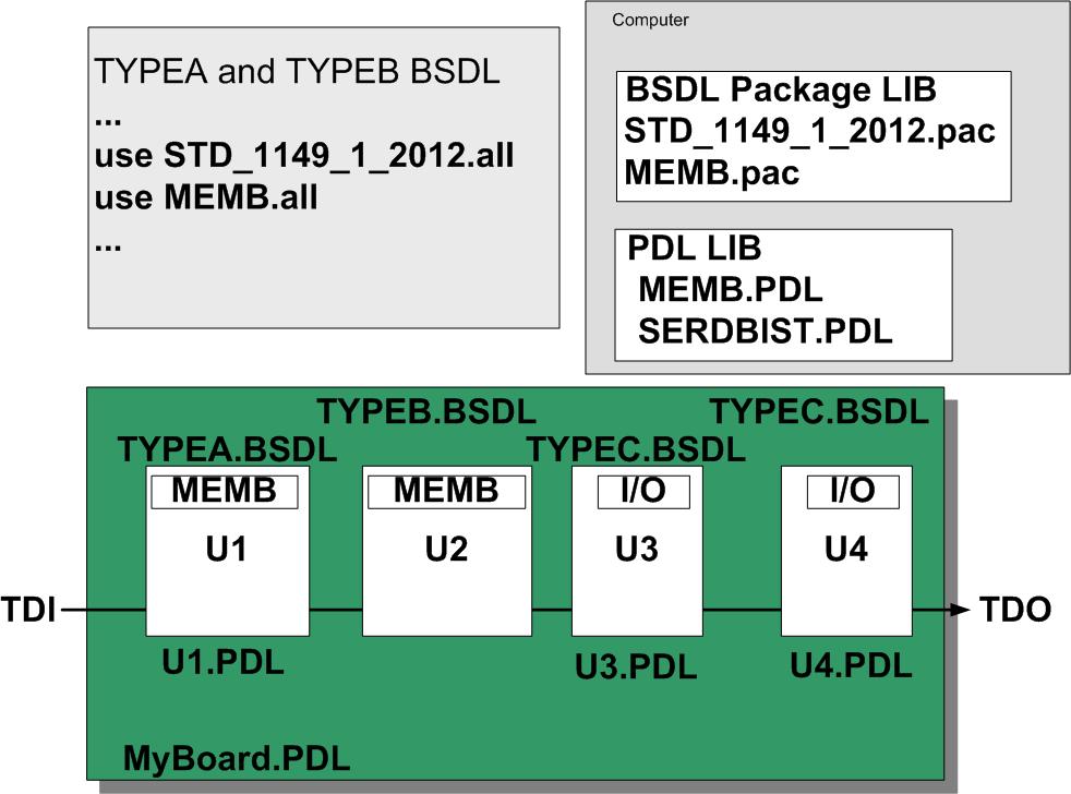
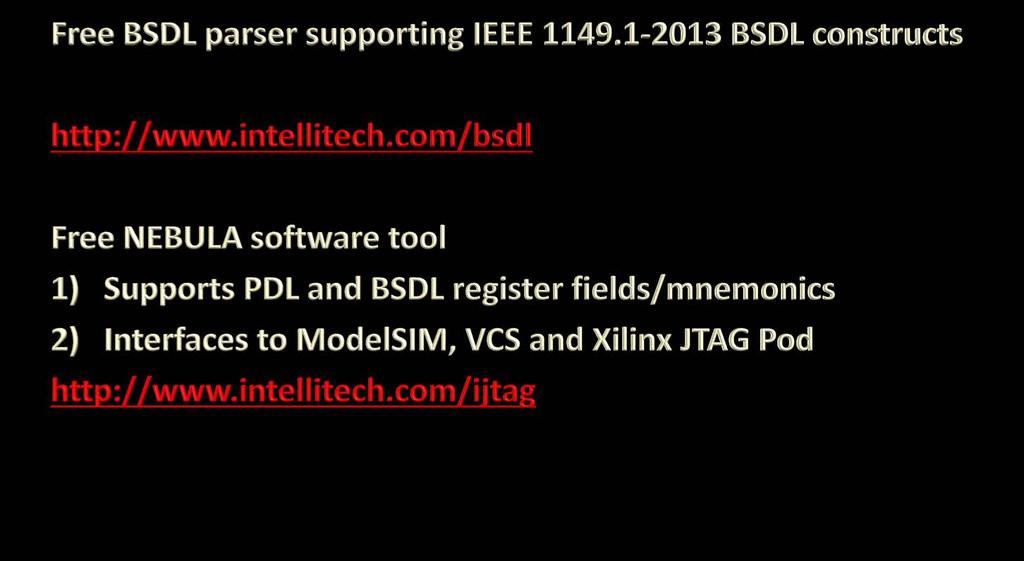
25 25
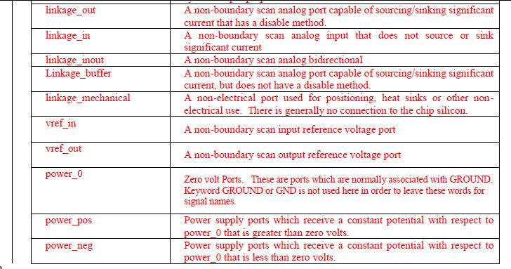
 B OUTPUT2 C Bidir")


26 2.5V INPUT ( Open0) A INPUT (Open1) B OUTPUT2 C Bidir with Pull0 D Bidir with Pull V POWER_POS INPUT ( PULL1) Bidir with Pull0 Control Obstacle 26

27 MODE=1 VDD HSIO D GND 27


28 BER XMIT BER RCVR 28
29 IC2 DC/DC Converter 3.3V BIDIR BIDIR BIDIR BIDIR A B C D POWER_POS INPUT LINKAGE_IN LINKAGE_IN LINKAGE_IN LINKAGE_IN IC1 VREF_IN VREF_OUT INPUT POWER_0 DC/DC Converter 2.5V 29
30 30
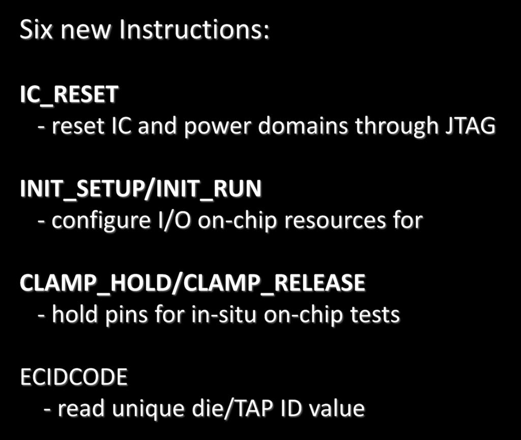
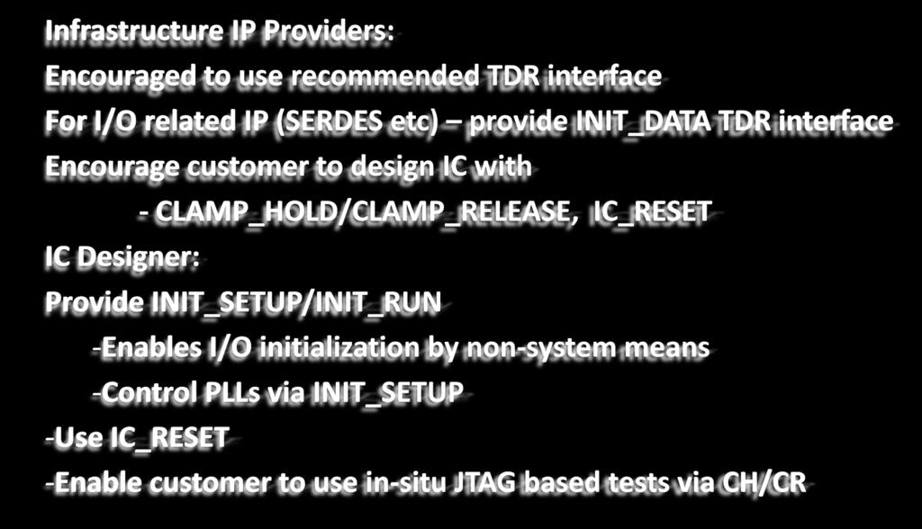
31 31
32 BSDL for Internal JTAG TDR registers - for BIST/PLLs/SERDES IP blocks MNEMONICS for JTAG registers - Easy to remember words Package files for on-chip Infrastructure IP blocks - self-contained definitions for IIP PDL Script files for device initialization and IIP access - operates on registers, packages, Mnemonics 32
33 33

 Logic BIST Memory BIST BIST Failure Data For ATE PCB")
34 BOUNDARY REGISTER INIT-DATA REGISTER 0 1 ADC DAC System Reset SysReset On-chip Reset via TAP PLL Protocol Swing ECID Unique ID 0 1 AC/DC Voltage Monitor PRBS CMMV PCB Level Obstacle User Defined Chain(s) Logic BIST Memory BIST BIST Failure Data For ATE PCB Level Obstacle IC1 IR & Decode & Muxing TAP 34
35 To next cell Mode G1 0 To System Logic 1 1D C1 ClockDR 1D C1 UpdateDR 35
36 BOUNDARY REGISTER INIT-DATA REGISTER 0 1 ADC DAC System Reset SysReset On-chip Reset via TAP PLL Protocol Swing ECID Unique ID 0 1 AC/DC Voltage Monitor PRBS CMMV PCB Level Obstacle User Defined Chain(s) Logic BIST Memory BIST BIST Failure Data For ATE PCB Level Obstacle IC1 IR & Decode & Muxing TAP 36
37 37
38 38
39 New standard INIT_DATA & INIT_STATUS TDRs New instructions, INIT_SETUP/INIT_RUN -Use between PRELOAD and EXTEST - Turn off PLLs -Setup I/Os (Vcm, Vswing, protocol. ) INIT_SETUP access INIT_DATA - Uses TAP, CE, power - INIT_DATA bits control the above INIT_RUN access INIT_Status register. Can clock TCK in RTI. - Pass/Fail, Done other bits as needed 39

40 Why can t I/O settings be delivered in BSDL? U1 PCIe U2 SRIO TypeC.BSDL IO1 U3 IO1 U4 TypeC.BSDL U3.PDL iproc init_setup {} { iwrite IO1 PCIe iapply } U4.PDL iproc init_setup {} { iwrite IO1 SRIO iapply } Board Test Engineer Developed via Software or from Templates from IC Vendor Board.PDL icall U3.init_setup icall U4.init_setup Board Test Engineer Developed via Board Test Software, Automatically, assisted or manually 40
41 Basic Register Fields attribute REGISTER_FIELDS of INIT_Example : entity is "init_data ( "& "(Clock[5] IS (504 DOWNTO 500) ), "& "(Protocol[3] IS (302 DOWNTO 300) ), "& "(Voltage[2] IS ( 101 DOWNTO 100) ), "& "(Reserved [20] IS ( 19 DOWNTO 0) ) "& ");" BSDL syntax for INIT_DATA and For Clause 9 user defined TDRs 41
42 MNEMONICS attribute REGISTER_MNEMONICS of SERDES : package is " Protocol ( & " OFF (000) <I/Os powered down>, "& " PCIe (001) <PCI Express>, "& " SATA (010) <SATA>, "& " SRIO (011) <Serial RapidIO>, "& " XAUI (100) <XAUI>, "& " Rsvd1 (101) <Undefined, do not use>"& )," & "Clockset ( " & " F125Mhz (00111), "& " F100Mhz (10101), "& " Illegal (00000) <Do not use!>)"; 42
43 Basic Register Fields with Mnemonics attribute REGISTER_FIELDS of INIT_Example : entity is "init_data ( "& "(Clock[5] IS (504 DOWNTO 500) Default(Clockset(100Mhz) ), "& "(Protocol[3] IS (302 DOWNTO 300) Default(Protocol (off) ), "& "(Voltage[2] IS ( 101 DOWNTO 100) RESETVAL(11) ), "& "(Reserved [20] IS ( 19 DOWNTO 0))"& ")" & mytdr ( "& "(Addr[64] IS (163 DOWNTO 100) ), "& (Data[64] IS (227 DOWNTO 164) ), "& (WE[1] IS (228) RESETVAL(1) ), "& (TempMON[7] IS (236 DOWNTO 229)) "& ); 43
44 44
45 Device PDL (Procedure Definition Language) - Board specific Proc init_setup {} { iwrite Clock F125Mhz # use of mnemonics iwrite Voltage 0H01 # use of values iwrite Protocol PCIe iapply } Proc init_status {} { iread Status(1) Pass iapply } # use of mnemonics 45
46 Some PDL Commands iwrite <reg> <value> mnemonic iread <reg> <expected> mnemonic iapply iprefix <dotted path> ireset iendstate RTI PDR irunloop <TCK-Count> icall <iproc name> itarget <instance> # perform DR scan RTI-RTI # iprefix bank0.serdes # Test Logic Reset # set end state # Loop in RTI 46
47 iprefix U1 # U1.LBIST # run some basic tests on registers iwrite LBIST RUN # bit-position independent regs iapply irunloop iread LBISTSTATUS PASS # check that LBIST passed iapply iwrite SWING S400MV # set differential Swing to 400mv iwrite PROTOCOL1 SRIO # set protocol to SRIO iapply iwrite CAMBIST RUN # execute CAM BIST iapply iread CAMSTATUS DONE 47

, SD_TX_B(0)),\"& \"SerDes01 (SD_RX(1),")
48 attribute REGISTER_PORT_ASSOCIATION ("& "SerDes00_PRBS (SD_RX(0), SD_RX_B(0), SD_TX(0), SD_TX_B(0)),"& "SerDes01 (SD_RX(1), SD_RX_B(1), SD_TX(1), SD_TX_B(1)) ; 48

49 3 SERDES with init_data Registers Common PLL 49
50 Package file including single SERDES segment -- and a 3 SERDES plus clock segment. -- Copywrong of the XYZ corp PACKAGE XYZ_IO IS USE Std_1149_1_2013.all; attribute REGISTER_MNEMONICS of XYZ_IO : package IS "SerDes_Protocol (off (000) <Powered down>, "& " PCIe (001) <PCIExpress>, "& " SATA (010) <SATA>, "& " SRIO (011) <Serial RapidIO>, "& " XAUI (101) <XAUI>, "& " Resvd1 (100) <Undefined behavior - Do Not Use>, "& " Resvd2 (11X) <Undefined behavior - Do Not Use>), "& "SerDes_TX_Outputs (off (00) <Powered down>, "& -- Output driver swing level " Full_Swing (01) <100% Swing>, "& " Swing_p75 (10) <75% Swing>, "& " Swing_p527 (11) <52.7% Swing - Not legal if XAUI is protocol>), "& 50
![attribute REGISTER_FIELDS of XYZ_IO : package IS "Channel [5] ( "& "Protocol[3] (2, 0, 1) IS DEFAULT (SerDes_Protocol (PCIe)) "& RESETVAL(SerDes_Protocol (off)), "& "TX_Swing [2] (3, 4) IS DEFAULT](/docs-images/87/96900126/images/51-5.jpg "(SerDes_TX_Outputs (off)) \"& \"), \"& www.intellitech.com END XYZ_IO; ----------------------------------------------------------------------------- --- PACKAGE BODY XYZ_IO IS USE Std_1149_1_2013.")
51 attribute REGISTER_FIELDS of XYZ_IO : package IS "Channel [5] ( "& "Protocol[3] (2, 0, 1) IS DEFAULT (SerDes_Protocol (PCIe)) "& RESETVAL(SerDes_Protocol (off)), "& "TX_Swing [2] (3, 4) IS DEFAULT (SerDes_TX_Outputs (off)) "& "), "& END XYZ_IO; PACKAGE BODY XYZ_IO IS USE Std_1149_1_2013.all; END XYZ_IO; 51
52 Register assembly bits predefined defined length calculated by BSDL reader Use XYZ_IO.all; Use XYZ_PLL.all; -- stuff removed for brevity attribute REGISTER_ASSEMBLY of INIT_Example : entity is "init_data ( "& (USING XYZ_PLL), & ( P1 is Settings), & ( USING XYZ_IO ), & ( Array SerDes(1 TO 2) is Channel), & ( dummy[1] ), & ( SerDes( 0) is Channel ), & ( reserved[105] ) & "); TDI Rsrvd SERDES SERDES SERDES PLL TDO 52

53 53


54 54
Using Test Access Standards Across The Product Lifecycle
 Using Test Access Standards Across The Product Lifecycle Andrew Richardson A.Richardson@enablingMNT.co.uk 1 Outline Background & Previous Work Revision - Boundary Scan Extension to ijtag IEEE1687 ijtag
Testing Sequential Logic. CPE/EE 428/528 VLSI Design II Intro to Testing (Part 2) Testing Sequential Logic (cont d) Testing Sequential Logic (cont d)
 Testing Sequential Logic (cont d) Testing Sequential Logic (cont d)") Testing Sequential Logic CPE/EE 428/528 VLSI Design II Intro to Testing (Part 2) Electrical and Computer Engineering University of Alabama in Huntsville In general, much more difficult than testing combinational
Testing Sequential Logic CPE/EE 428/528 VLSI Design II Intro to Testing (Part 2) Electrical and Computer Engineering University of Alabama in Huntsville In general, much more difficult than testing combinational
Using the XC9500/XL/XV JTAG Boundary Scan Interface
 Application Note: XC95/XL/XV Family XAPP69 (v3.) December, 22 R Using the XC95/XL/XV JTAG Boundary Scan Interface Summary This application note explains the XC95 /XL/XV Boundary Scan interface and demonstrates
Section 24. Programming and Diagnostics
 Section. and Diagnostics HIGHLIGHTS This section of the manual contains the following topics:.1 Introduction... -2.2 In-Circuit Serial... -2.3 Enhanced In-Circuit Serial... -5.4 JTAG Boundary Scan... -6.5
Section 24. Programming and Diagnostics
 Section. Programming and Diagnostics HIGHLIGHTS This section of the manual contains the following topics:.1 Introduction... -2.2 In-Circuit Serial Programming... -3.3 Enhanced In-Circuit Serial Programming...
SV1C Personalized SerDes Tester
 SV1C Personalized SerDes Tester Data Sheet SV1C Personalized SerDes Tester Data Sheet Revision: 1.0 2013-02-27 Revision Revision History Date 1.0 Document release Feb 27, 2013 The information in this
7 Nov 2017 Testing and programming PCBA s
 7 Nov 207 Testing and programming PCBA s Rob Staals JTAG Technologies Email: robstaals@jtag.com JTAG Technologies The importance of Testing Don t ship bad products to your customers, find problems before
Ilmenau, 9 Dec 2016 Testing and programming PCBA s. 1 JTAG Technologies
 Ilmenau, 9 Dec 206 Testing and programming PCBA s JTAG Technologies The importance of Testing Don t ship bad products to your customers, find problems before they do. DOA s (Death On Arrival) lead to huge
Introduction to JTAG / boundary scan-based testing for 3D integrated systems. (C) GOEPEL Electronics -
 GOEPEL Electronics -") Introduction to JTAG / boundary scan-based testing for 3D integrated systems (C) 2011 - GOEPEL Electronics - www.goepelusa.com Who is GOEPEL? World Headquarters: GÖPEL electronic GmbH Göschwitzer Straße
Introduction to JTAG / boundary scan-based testing for 3D integrated systems (C) 2011 - GOEPEL Electronics - www.goepelusa.com Who is GOEPEL? World Headquarters: GÖPEL electronic GmbH Göschwitzer Straße
Overview of BDM nc. The IEEE JTAG specification is also recommended reading for those unfamiliar with JTAG. 1.2 Overview of BDM Before the intr
 Application Note AN2387/D Rev. 0, 11/2002 MPC8xx Using BDM and JTAG Robert McEwan NCSD Applications East Kilbride, Scotland As the technical complexity of microprocessors has increased, so too has the
BSDL Validation: A Case Study
 ASSET InterTech, Inc. Validation: A Case Study Michael R. Johnson Sr. Applications Engineer ASSET InterTech, Inc. Agilent Boundary Scan User Group Meeting December 15, 2008 About The Presenter Michael
the Boundary Scan perspective
 the Boundary Scan perspective Rik Doorneweert, JTAG Technologies rik@jtag.com www.jtag.com Subjects Economics of testing Test methods and strategy Boundary scan at: Component level Board level System level
12. IEEE (JTAG) Boundary-Scan Testing for the Cyclone III Device Family
 Boundary-Scan Testing for the Cyclone III Device Family") December 2011 CIII51014-2.3 12. IEEE 1149.1 (JTAG) Boundary-Scan Testing for the Cyclone III Device Family CIII51014-2.3 This chapter provides guidelines on using the IEEE Std. 1149.1 boundary-scan test
December 2011 CIII51014-2.3 12. IEEE 1149.1 (JTAG) Boundary-Scan Testing for the Cyclone III Device Family CIII51014-2.3 This chapter provides guidelines on using the IEEE Std. 1149.1 boundary-scan test
18 Nov 2015 Testing and Programming PCBA s. 1 JTAG Technologies
 8 Nov 25 Testing and Programming PCBA s JTAG Technologies The importance of Testing Don t ship bad products to your customers, find problems before they do. DOA s (Death On Arrival) lead to huge costs
Remote Diagnostics and Upgrades
 Remote Diagnostics and Upgrades Tim Pender -Eastman Kodak Company 10/03/03 About this Presentation Motivation for Remote Diagnostics Reduce Field Maintenance costs Product needed to support 100 JTAG chains
Chapter 19 IEEE Test Access Port (JTAG)
") Chapter 9 IEEE 49. Test Access Port (JTAG) This chapter describes configuration and operation of the MCF537 JTAG test implementation. It describes the use of JTAG instructions and provides information
Chapter 9 IEEE 49. Test Access Port (JTAG) This chapter describes configuration and operation of the MCF537 JTAG test implementation. It describes the use of JTAG instructions and provides information
C65SPACE-HSSL Gbps multi-rate, multi-lane, SerDes macro IP. Description. Features
 6.25 Gbps multi-rate, multi-lane, SerDes macro IP Data brief Txdata1_in Tx1_clk Bist1 Rxdata1_out Rx1_clk Txdata2_in Tx2_clk Bist2 Rxdata2_out Rx2_clk Txdata3_in Tx3_clk Bist3 Rxdata3_out Rx3_clk Txdata4_in
16 Dec Testing and Programming PCBA s. 1 JTAG Technologies
 6 Dec 24 Testing and Programming PCBA s JTAG Technologies The importance of Testing Don t ship bad products to your customers, find problems before they do. DOA s (Death On Arrival) lead to huge costs
SµMMIT E & LXE/DXE JTAG Testability for the SJ02 Die
 UTMC Application Note SµMMIT E & LXE/DXE JTAG Testability for the SJ02 Die JTAG Instructions: JTAG defines seven (7) public instructions as follows: Instruction Status UTMC Code msb..lsb SµMMIT Status
Using IEEE Boundary Scan (JTAG) With Cypress Ultra37000 CPLDs
 With Cypress Ultra37000 CPLDs") Using IEEE 49. Boundary Scan (JTAG) With Cypress Ultra37 CPLDs Introduction As Printed Circuit Boards (PCBs) have become multi-layered with double-sided component mounting and Integrated Circuits have
Using IEEE 49. Boundary Scan (JTAG) With Cypress Ultra37 CPLDs Introduction As Printed Circuit Boards (PCBs) have become multi-layered with double-sided component mounting and Integrated Circuits have
Chapter 10 Exercise Solutions
 VLSI Test Principles and Architectures Ch. 10 oundary Scan & Core-ased Testing P. 1/10 Chapter 10 Exercise Solutions 10.1 The following is just an example for testing chips and interconnects on a board.
of Boundary Scan techniques.
 SMT TEHNOLOGY Boundary Scan Techniques for Test Coverage Improvement When discussing the JTAG protocol, most engineers immediately think of In System Programming procedures. Indeed, there are numerous
JRC ( JTAG Route Controller ) Data Sheet
 Data Sheet") JRC ( JTAG Route Controller ) Data Sheet ATLAS TGC Electronics Group September 5, 2002 (version 1.1) Author : Takashi Takemoto Feature * JTAG signal router with two inputs and seven outputs. * Routing
JRC ( JTAG Route Controller ) Data Sheet ATLAS TGC Electronics Group September 5, 2002 (version 1.1) Author : Takashi Takemoto Feature * JTAG signal router with two inputs and seven outputs. * Routing
BABAR IFR TDC Board (ITB): system design
: system design") BABAR IFR TDC Board (ITB): system design Version 1.1 12 december 1997 G. Crosetti, S. Minutoli, E. Robutti I.N.F.N. Genova 1. Introduction TDC readout of the IFR will be used during BABAR data taking to
BABAR IFR TDC Board (ITB): system design Version 1.1 12 december 1997 G. Crosetti, S. Minutoli, E. Robutti I.N.F.N. Genova 1. Introduction TDC readout of the IFR will be used during BABAR data taking to
SV1C Personalized SerDes Tester. Data Sheet
 SV1C Personalized SerDes Tester Data Sheet Table of Contents 1 Table of Contents Table of Contents Table of Contents... 2 List of Figures... 3 List of Tables... 3 Introduction... 4 Overview... 4 Key Benefits...
Using the XSV Board Xchecker Interface
 Using the XSV Board Xchecker Interface May 1, 2001 (Version 1.0) Application Note by D. Vanden Bout Summary This application note shows how to configure the XC9510 CPLD on the XSV Board to enable the programming
BTW03 DESIGN CONSIDERATIONS IN USING AS A BACKPLANE TEST BUS International Test Conference. Pete Collins
 2003 International Test Conference DESIGN CONSIDERATIONS IN USING 1149.1 AS A BACKPLANE TEST BUS Pete Collins petec@jtag.co.uk JTAG TECHNOLOGIES BTW03 PURPOSE The purpose of this presentation is to discuss
UNIT IV CMOS TESTING. EC2354_Unit IV 1
 UNIT IV CMOS TESTING EC2354_Unit IV 1 Outline Testing Logic Verification Silicon Debug Manufacturing Test Fault Models Observability and Controllability Design for Test Scan BIST Boundary Scan EC2354_Unit
Lecture 17: Introduction to Design For Testability (DFT) & Manufacturing Test
 & Manufacturing Test") Lecture 17: Introduction to Design For Testability (DFT) & Manufacturing Test Mark McDermott Electrical and Computer Engineering The University of Texas at Austin Agenda Introduction to testing Logical
Lecture 17: Introduction to Design For Testability (DFT) & Manufacturing Test Mark McDermott Electrical and Computer Engineering The University of Texas at Austin Agenda Introduction to testing Logical
Unit V Design for Testability
 Unit V Design for Testability Outline Testing Logic Verification Silicon Debug Manufacturing Test Fault Models Observability and Controllability Design for Test Scan BIST Boundary Scan Slide 2 Testing
TKK S ASIC-PIIRIEN SUUNNITTELU
 Design TKK S-88.134 ASIC-PIIRIEN SUUNNITTELU Design Flow 3.2.2005 RTL Design 10.2.2005 Implementation 7.4.2005 Contents 1. Terminology 2. RTL to Parts flow 3. Logic synthesis 4. Static Timing Analysis
A Briefing on IEEE Standard Test Access Port And Boundary-Scan Architecture ( AKA JTAG )
") A Briefing on IEEE 1149.1 1990 Standard Test Access Port And Boundary-Scan Architecture ( AKA JTAG ) Summary With the advent of large Ball Grid Array (BGA) and fine pitch SMD semiconductor devices the
A Briefing on IEEE 1149.1 1990 Standard Test Access Port And Boundary-Scan Architecture ( AKA JTAG ) Summary With the advent of large Ball Grid Array (BGA) and fine pitch SMD semiconductor devices the
JTAG Test Controller
 Description JTAG Test Controller The device provides an interface between the 60x bus on the Motorola MPC8260 processor and two totally independent IEEE1149.1 interfaces, namely, the primary and secondary
Product Update. JTAG Issues and the Use of RT54SX Devices
 Product Update Revision Date: September 2, 999 JTAG Issues and the Use of RT54SX Devices BACKGROUND The attached paper authored by Richard B. Katz of NASA GSFC and J. J. Wang of Actel describes anomalies
Comparing JTAG, SPI, and I2C
 Comparing JTAG, SPI, and I2C Application by Russell Hanabusa 1. Introduction This paper discusses three popular serial buses: JTAG, SPI, and I2C. A typical electronic product today will have one or more
3. Configuration and Testing
 3. Configuration and Testing C51003-1.4 IEEE Std. 1149.1 (JTAG) Boundary Scan Support All Cyclone devices provide JTAG BST circuitry that complies with the IEEE Std. 1149.1a-1990 specification. JTAG boundary-scan
Subjects. o JTAG Technologies (Rik Doorneweert, Area Manager) o JTAG Technologies B.V. activities o Introduction to (classic) Boundary Scan
 o JTAG Technologies B.V. activities o Introduction to (classic) Boundary Scan") Subjects o JTAG Technologies (Rik Doorneweert, Area Manager) o JTAG Technologies B.V. activities o Introduction to (classic) Boundary Scan o Grass Valley Breda(Camera division) (Khaled Sarsam, Test Automation
Subjects o JTAG Technologies (Rik Doorneweert, Area Manager) o JTAG Technologies B.V. activities o Introduction to (classic) Boundary Scan o Grass Valley Breda(Camera division) (Khaled Sarsam, Test Automation
Device 1 Device 2 Device 3 Device 4
 APPLICATION NOTE 0 The Tagalyzer - A JTAG Boundary Scan Debug Tool XAPP 103 March 1, 2007 (Version 1.1) 0 3* Application Note Summary The Tagalyzer is a diagnostic tool that helps debug long JTAG boundary
Digital Integrated Circuits Lecture 19: Design for Testability
 Digital Integrated Circuits Lecture 19: Design for Testability Chih-Wei Liu VLSI Signal Processing LAB National Chiao Tung University cwliu@twins.ee.nctu.edu.tw DIC-Lec19 cwliu@twins.ee.nctu.edu.tw 1 Outline
IIIHIII III. Signal in. BIST ShiftDR United States Patent (19) Tsai et al. Out Mode Signal out. mclockdr. SCOn
 Tsai et al. Out Mode Signal out. mclockdr. SCOn") United States Patent (19) Tsai et al. 54 IEEE STD. 1149.1 BOUNDARY SCAN CIRCUIT CAPABLE OF BUILT-IN SELF-TESTING 75) Inventors: Ching-Hong Tsai, Fang-Diahn Guo; Jin-Hua Hong; Cheng-Wen Wu, all of Hsinchu,
United States Patent (19) Tsai et al. 54 IEEE STD. 1149.1 BOUNDARY SCAN CIRCUIT CAPABLE OF BUILT-IN SELF-TESTING 75) Inventors: Ching-Hong Tsai, Fang-Diahn Guo; Jin-Hua Hong; Cheng-Wen Wu, all of Hsinchu,
CMOS Testing-2. Design for testability (DFT) Design and Test Flow: Old View Test was merely an afterthought. Specification. Design errors.
 Design and Test Flow: Old View Test was merely an afterthought. Specification. Design errors.") Design and test CMOS Testing- Design for testability (DFT) Scan design Built-in self-test IDDQ testing ECE 261 Krish Chakrabarty 1 Design and Test Flow: Old View Test was merely an afterthought Specification
Design and test CMOS Testing- Design for testability (DFT) Scan design Built-in self-test IDDQ testing ECE 261 Krish Chakrabarty 1 Design and Test Flow: Old View Test was merely an afterthought Specification
Memec Spartan-II LC User s Guide
 Memec LC User s Guide July 21, 2003 Version 1.0 1 Table of Contents Overview... 4 LC Development Board... 4 LC Development Board Block Diagram... 6 Device... 6 Clock Generation... 7 User Interfaces...
XJTAG DFT Assistant for
 XJTAG DFT Assistant for Installation and User Guide Version 1.0 enquiries@xjtag.com Table of Contents SECTION PAGE 1. Introduction...3 2. Installation...3 3. Quick Start Guide...3 4. User Guide...4 4.1.
SERDES Eye/Backplane Demo for the LatticeECP3 Serial Protocol Board User s Guide
 for the LatticeECP3 Serial Protocol Board User s Guide March 2011 UG24_01.4 Introduction This document provides technical information and instructions on using the LatticeECP3 SERDES Eye/Backplane Demo
FPGA Design with VHDL
 FPGA Design with VHDL Justus-Liebig-Universität Gießen, II. Physikalisches Institut Ming Liu Dr. Sören Lange Prof. Dr. Wolfgang Kühn ming.liu@physik.uni-giessen.de Lecture Digital design basics Basic logic
SµMMIT E & LXE/DXE Built-In-Self-Test Functionality for the JA01 Die
 UTMC Application Note SµMMIT E & LXE/DXE Built-In-Self-Test Functionality for the JA01 Die JTAG Instructions: JTAG defines seven (7) public instructions as follows: Instruction Status UTMC Code msb..lsb
Achieving Timing Closure in ALTERA FPGAs
 Achieving Timing Closure in ALTERA FPGAs Course Description This course provides all necessary theoretical and practical know-how to write system timing constraints for variety designs in ALTERA FPGAs.
Debugging IDT S-RIO Gen2 Switches Using RapidFET JTAG
 Titl Debugging IDT S-RIO Gen2 Switches Using RapidFET JTAG Application Note March 29, 2012 About this Document This document discusses common problems that are encountered when debugging with a board that
Y. Tsiatouhas. VLSI Systems and Computer Architecture Lab. Boundary Scan (JTAG ) 2
 2") CMOS INTEGRATE CIRCUIT EGN TECHNIUES University of Ioannina Boundary Scan Testing (JTAG ΙΕΕΕ 49 std) ept of Computer Science and Engineering Y Tsiatouhas CMOS Integrated Circuit esign Techniques VL Systems
CMOS INTEGRATE CIRCUIT EGN TECHNIUES University of Ioannina Boundary Scan Testing (JTAG ΙΕΕΕ 49 std) ept of Computer Science and Engineering Y Tsiatouhas CMOS Integrated Circuit esign Techniques VL Systems
Combating Closed Eyes Design & Measurement of Pre-Emphasis and Equalization for Lossy Channels
 Combating Closed Eyes Design & Measurement of Pre-Emphasis and Equalization for Lossy Channels Why Test the Receiver? Serial Data communications standards have always specified both the transmitter and
Combating Closed Eyes Design & Measurement of Pre-Emphasis and Equalization for Lossy Channels
 Combating Closed Eyes Design & Measurement of Pre-Emphasis and Equalization for Lossy Channels Why Test the Receiver? Serial Data communications standards have always specified both the transmitter and
Prototyping Solutions For New Wireless Standards
 Prototyping Solutions For New Wireless Standards Christoph Juchems IAF Institute For Applied Radio System Technology Berliner Str. 52 J D-38104 Braunschweig Germany www.iaf-bs.de Introduction IAF Institute
University of Arizona January 18, 2000 Joel Steinberg Rev. 1.6
 I/O Specification for Serial Receiver Daughter Board (PCB-0140-RCV) (Revised January 18, 2000) 1.0 Introduction The Serial Receiver Daughter Board accepts an 8b/10b encoded serial data stream, operating
Document Part Number: Copyright 2010, Corelis Inc.
 CORELIS Low Voltage Adapter Low Voltage Adapter Boundary-Scan Interface User s Manual Document Part Number: 70398 Copyright 2010, Corelis Inc. Corelis, Inc. 12607 Hiddencreek Way Cerritos, CA 90703-2146
IEEE Standard (JTAG) in the Axcelerator Family
 in the Axcelerator Family") Application Note AC27 IEEE Standard 49. (JTAG) in the Axcelerator Family Introduction Testing modern loaded circuit boards has become extremely expensive and very difficult to perform. The rapid development
Application Note AC27 IEEE Standard 49. (JTAG) in the Axcelerator Family Introduction Testing modern loaded circuit boards has become extremely expensive and very difficult to perform. The rapid development
Logic Analysis Basics
 Logic Analysis Basics September 27, 2006 presented by: Alex Dickson Copyright 2003 Agilent Technologies, Inc. Introduction If you have ever asked yourself these questions: What is a logic analyzer? What
Logic Analysis Basics
 Logic Analysis Basics September 27, 2006 presented by: Alex Dickson Copyright 2003 Agilent Technologies, Inc. Introduction If you have ever asked yourself these questions: What is a logic analyzer? What
ASNT8140. ASNT8140-KMC DC-23Gbps PRBS Generator with the (x 7 + x + 1) Polynomial. vee. vcc qp. vcc. vcc qn. qxorp. qxorn. vee. vcc rstn_p.
 Polynomial. vee. vcc qp. vcc. vcc qn. qxorp. qxorn. vee. vcc rstn_p.") ASNT8140-KMC DC-23Gbps PRBS Generator with the (x 7 + x + 1) Polynomial Full-length (2 7-1) pseudo-random binary sequence (PRBS) generator DC to 23Gbps output data rate Additional output delayed by half
ASNT8140-KMC DC-23Gbps PRBS Generator with the (x 7 + x + 1) Polynomial Full-length (2 7-1) pseudo-random binary sequence (PRBS) generator DC to 23Gbps output data rate Additional output delayed by half
XJTAG DFT Assistant for
 XJTAG DFT Assistant for Installation and User Guide Version 2 enquiries@xjtag.com Table of Contents SECTION PAGE 1. Introduction...3 2. Installation...3 3. Quick Start Guide...4 4. User Guide...4 4.1.
Transmission of High-Speed Serial Signals Over Common Cable Media
 August 00 Introduction Technical Note TN066 Designers are often faced with moving serial data from one location to another, over moderate distances, and in the most efficient manner. Transmitting large
SignalTap Plus System Analyzer
 SignalTap Plus System Analyzer June 2000, ver. 1 Data Sheet Features Simultaneous internal programmable logic device (PLD) and external (board-level) logic analysis 32-channel external logic analyzer 166
SERDES Eye/Backplane Demo for the LatticeECP3 Versa Evaluation Board User s Guide
 SERDES Eye/Backplane Demo for the LatticeECP3 Versa Evaluation Board User s Guide May 2011 UG44_01.1 Introduction This document provides technical information and instructions on using the LatticeECP3
Powerful Software Tools and Methods to Accelerate Test Program Development A Test Systems Strategies, Inc. (TSSI) White Paper.
 White Paper.") Powerful Software Tools and Methods to Accelerate Test Program Development A Test Systems Strategies, Inc. (TSSI) White Paper Abstract Test costs have now risen to as much as 50 percent of the total manufacturing
Powerful Software Tools and Methods to Accelerate Test Program Development A Test Systems Strategies, Inc. (TSSI) White Paper Abstract Test costs have now risen to as much as 50 percent of the total manufacturing
In-System Programmability Guidelines
 In-System Programmability Guidelines May 1999, ver. 3 Application Note 100 Introduction As time-to-market pressures increase, design engineers require advanced system-level products to ensure problem-free
XJTAG DFT Assistant for
 XJTAG DFT Assistant for Installation and User Guide Version 2 enquiries@xjtag.com Table of Contents SECTION PAGE 1. Introduction...3 2. Installation...3 3. Quick Start Guide...3 4. User Guide...4 4.1.
12-Port Serial RapidIO Switch
 12-Port Serial RapidIO Switch Datasheet 80KSW0004 1 Device Overview The CPS-12, device number IDT80KSW0004, is a serial RapidIO (srio) switch whose functionality is central to routing packets for distribution
XJTAG DFT Assistant for
 XJTAG DFT Assistant for Installation and User Guide Version 2 enquiries@xjtag.com Table of Contents SECTION PAGE 1. Introduction...3 2. Installation...3 3. Quick Start Guide...3 4. User Guide...4 4.1.
OpenOCD - Beyond Simple Software Debugging
 OpenOCD - Beyond Simple Software Debugging Oleksij Rempel o.rempel@pengutronix.de https://www.pengutronix.de Why I use OpenOCD? Reverse engineering and for fun This is the main motivation behind this talk
Practical De-embedding for Gigabit fixture. Ben Chia Senior Signal Integrity Consultant 5/17/2011
 Practical De-embedding for Gigabit fixture Ben Chia Senior Signal Integrity Consultant 5/17/2011 Topics Why De-Embedding/Embedding? De-embedding in Time Domain De-embedding in Frequency Domain De-embedding
Laboratory 4. Figure 1: Serdes Transceiver
 Laboratory 4 The purpose of this laboratory exercise is to design a digital Serdes In the first part of the lab, you will design all the required subblocks for the digital Serdes and simulate them In part
Scan. This is a sample of the first 15 pages of the Scan chapter.
 Scan This is a sample of the first 15 pages of the Scan chapter. Note: The book is NOT Pinted in color. Objectives: This section provides: An overview of Scan An introduction to Test Sequences and Test
AMI Modeling Methodology and Measurement Correlation of a 6.25Gb/s Link
 May 26th, 2011 DAC IBIS Summit June 2011 AMI Modeling Methodology and Measurement Correlation of a 6.25Gb/s Link Ryan Coutts Antonis Orphanou Manuel Luschas Amolak Badesha Nilesh Kamdar Agenda Correlation
Chrontel CH7015 SDTV / HDTV Encoder
 Chrontel Preliminary Brief Datasheet Chrontel SDTV / HDTV Encoder Features 1.0 GENERAL DESCRIPTION VGA to SDTV conversion supporting graphics resolutions up to 104x768 Analog YPrPb or YCrCb outputs for
ontap BOUNDARY SCAN SOFTWARE PRODUCT FEATURES AND SCREEN TOUR FLYNN SYSTEMS CORP.
 ontap BOUNDARY SCAN SOFTWARE PRODUCT FEATURES AND SCREEN TOUR FLYNN SYSTEMS CORP. PROVIDING BOUNDARY SCAN SOLUTIONS SINCE 2000 1 ontap Product Documentation Table of Contents Introduction... 4 Overview...
Lecture 18 Design For Test (DFT)
") Lecture 18 Design For Test (DFT) Xuan Silvia Zhang Washington University in St. Louis http://classes.engineering.wustl.edu/ese461/ ASIC Test Two Stages Wafer test, one die at a time, using probe card production
Lecture 18 Design For Test (DFT) Xuan Silvia Zhang Washington University in St. Louis http://classes.engineering.wustl.edu/ese461/ ASIC Test Two Stages Wafer test, one die at a time, using probe card production
Extending JTAG for Testing Signal Integrity in SoCs
 Extending JTAG for Testing Signal Integrity in SoCs N. Ahmed, M. Tehranipour, M. Nourani Center for Integrated Circuits & Systems The University of Texas at Dallas Richardson, TX 7583-688 nxa86,mht2,nourani
XJTAG. Boundary Scan Tool. diagnosys.com
 XJTAG Boundary Scan Tool diagnosys.com XJLink Overview The XJLink is a small, portable, USB 2.0 to JTAG adapter that provides a high speed interface (480Mbps) to the JTAG chain. The small, lightweight
V6118 EM MICROELECTRONIC - MARIN SA. 2, 4 and 8 Mutiplex LCD Driver
 EM MICROELECTRONIC - MARIN SA 2, 4 and 8 Mutiplex LCD Driver Description The is a universal low multiplex LCD driver. The version 2 drives two ways multiplex (two blackplanes) LCD, the version 4, four
Performance Modeling and Noise Reduction in VLSI Packaging
 Performance Modeling and Noise Reduction in VLSI Packaging Ph.D. Defense Brock J. LaMeres University of Colorado October 7, 2005 October 7, 2005 Performance Modeling and Noise Reduction in VLSI Packaging
K.T. Tim Cheng 07_dft, v Testability
 K.T. Tim Cheng 07_dft, v1.0 1 Testability Is concept that deals with costs associated with testing. Increase testability of a circuit Some test cost is being reduced Test application time Test generation
ACS College of Engineering. Department of Biomedical Engineering. HDL pre lab questions ( ) Cycle-1
 Cycle-1") ACS College of Engineering Department of Biomedical Engineering HDL pre lab questions (2015-2016) Cycle-1 1. What is truth table? 2. Which gates are called universal gates? 3. Define HDL? 4. What is the
ACS College of Engineering Department of Biomedical Engineering HDL pre lab questions (2015-2016) Cycle-1 1. What is truth table? 2. Which gates are called universal gates? 3. Define HDL? 4. What is the
Transmission of High-Speed Serial Signals Over Common Cable Media
 July 008 Introduction Technical Note TN066 Designers are often faced with moving serial data from one location to another, over moderate distances, and in the most efficient manner. Transmitting large
ASNT8142-KMC Generator of DC-to-23Gbps PRBS with Selectable Polynomials
 ASNT8142-KMC Generator of DC-to-23Gbps PRBS with Selectable Polynomials Full-length (2 15-1) or (2 7-1) pseudo-random binary sequence (PRBS) generator Selectable power of the Polynomial DC to 23Gbps output
DEPARTMENT OF ELECTRICAL &ELECTRONICS ENGINEERING DIGITAL DESIGN
 DEPARTMENT OF ELECTRICAL &ELECTRONICS ENGINEERING DIGITAL DESIGN Assoc. Prof. Dr. Burak Kelleci Spring 2018 OUTLINE Synchronous Logic Circuits Latch Flip-Flop Timing Counters Shift Register Synchronous
10Gbps SFP+ Optical Transceiver, 10km Reach
 10Gbps SFP+ Optical Transceiver, 10km Reach Features Optical interface compliant to IEEE 802.3ae 10GBASE-LR Electrical interface compliant to SFF-8431 Hot Pluggable 1310nm DFB transmitter, PIN photo-detector
Complete 10-Bit, 25 MHz CCD Signal Processor AD9943
 a FEATURES 25 MSPS Correlated Double Sampler (CDS) 6 db to 40 db 10-Bit Variable Gain Amplifier (VGA) Low Noise Optical Black Clamp Circuit Preblanking Function 10-Bit, 25 MSPS A/D Converter No Missing
Raspberry Pi debugging with JTAG
 Arseny Kurnikov Aalto University December 13, 2013 Outline JTAG JTAG on RPi Linux kernel debugging JTAG Joint Test Action Group is a standard for a generic transport interface for integrated circuits.
Complete 10-Bit/12-Bit, 25 MHz CCD Signal Processor AD9943/AD9944
 a FEATURES 25 MSPS Correlated Double Sampler (CDS) 6 db to 40 db 10-Bit Variable Gain Amplifier (VGA) Low Noise Optical Black Clamp Circuit Preblanking Function 10-Bit (AD9943), 12-Bit (AD9944), 25 MSPS
System IC Design: Timing Issues and DFT. Hung-Chih Chiang
 Wireless Information Transmission System Lab. System IC esign: Timing Issues and FT Hung-Chih Chiang Institute of Communications Engineering National Sun Yat-sen University SoC Timing Issues Outline Timing
Complete 12-Bit 40 MHz CCD Signal Processor AD9945
 Complete 12-Bit 40 MHz CCD Signal Processor AD9945 FEATURES 40 MSPS Correlated Double Sampler (CDS) 6 db to 40 db 10-Bit Variable Gain Amplifier (VGA) Low Noise Optical Black Clamp Circuit Preblanking
Universal ByteBlaster
 Universal ByteBlaster Hardware Manual June 20, 2005 Revision 1.1 Amfeltec Corp. www.amfeltec.com Copyright 2008 Amfeltec Corp. 35 Fifefield dr. Maple, L6A 1J2 Contents Contents 1 About this Document...
10-Quad RapidIO Switch
 1-Quad RapidIO Switch Datasheet 8KSW5 1 Device Overview The CPS-1Q (8KSW5) is a serial RapidIO switch whose functionality is central to routing packets for distribution among DSPs, processors, FPGAs, other
Description of the Synchronization and Link Board
 Available on CMS information server CMS IN 2005/007 March 8, 2005 Description of the Synchronization and Link Board ECAL and HCAL Interface to the Regional Calorimeter Trigger Version 3.0 (SLB-S) PMC short
ECE 372 Microcontroller Design
 E.g. Port A, Port B Used to interface with many devices Switches LEDs LCD Keypads Relays Stepper Motors Interface with digital IO requires us to connect the devices correctly and write code to interface
Ashling Product Brief APB219 v1.0.3, 12 th October 2018
 Ashling Product Brief APB219 v1.0.3, 12 th October 2018 Using Ultra-XD for Synopsys DesignWare ARC Cores with the MetaWare Debugger Contents 1. Introduction 2 2. Installation and Configuration 3 2.1 Installing
Tools to Debug Dead Boards
 Tools to Debug Dead Boards Hardware Prototype Bring-up Ryan Jones Senior Application Engineer Corelis 1 Boundary-Scan Without Boundaries click to start the show Webinar Outline What is a Dead Board? Prototype
GHz Sampling Design Challenge
 GHz Sampling Design Challenge 1 National Semiconductor Ghz Ultra High Speed ADCs Target Applications Test & Measurement Communications Transceivers Ranging Applications (Lidar/Radar) Set-top box direct
Adding Analog and Mixed Signal Concerns to a Digital VLSI Course
 Session Number 1532 Adding Analog and Mixed Signal Concerns to a Digital VLSI Course John A. Nestor and David A. Rich Department of Electrical and Computer Engineering Lafayette College Abstract This paper
COPYRIGHT 2011 AXON DIGITAL DESIGN BV ALL RIGHTS RESERVED
 GFS-HFS-SFS100/110 3Gb/s, HD, SD frame synchronizer with optional audio shuffler A Synapse product COPYRIGHT 2011 AXON DIGITAL DESIGN BV ALL RIGHTS RESERVED NO PART OF THIS DOCUMENT MAY BE REPRODUCED IN
Receiver Testing to Third Generation Standards. Jim Dunford, October 2011
 Receiver Testing to Third Generation Standards Jim Dunford, October 2011 Agenda 1.Introduction 2. Stressed Eye 3. System Aspects 4. Beyond Compliance 5. Resources 6. Receiver Test Demonstration PCI Express