Enabling Paper-Like Displays Roll-to-Roll Manufacturing of Display Backplanes. Hewlett-Packard Company, Palo Alto, CA. Phicot Inc, Ames, IA
|
|
|
- Sibyl Griffith
- 6 years ago
- Views:
Transcription
1 Enabling Paper-Like Displays Roll-to-Roll Manufacturing of Display Backplanes Carl Taussig, Bob Cobene, Rich Elder, Warren Jackson, Mehrban Jam, Albert Jeans, Hao Luo, Ping Mei, Craig Perlov, Hewlett-Packard Company, Palo Alto, CA Frank Jeffrey, Marcia Almanza-Workman, Kelly Beacom, Steve Braymen, Bob Garcia, Jason Hauschildt, Han-Jun Kim, Ohseung Kwon, Don Larson, Phicot Inc, Ames, IA
2 Outline Introduction What are the key attributes of a paper-like display Why we need paper-like displays High Performance Reflective Color Self-Aligned Imprint Lithography (SAIL) Benefits and challenges of roll-to-roll (R2R) manufacturing SAIL basics green manufacturing for green products toolset for 1/3m wide line world s first R2R active matrix displays ZXO based TFTs for enhanced performance


3 What is a Paper-Like Display? Paper Paper-like display Conventional display viewability Reflective: good in bright light as well as indoors Reflective; like paper Typically emissive or transmissive, not good in bright light form factor Paper is light, flexible, and rugged Plastic is light, flexible, and rugged Glass is fragile and heavy cost $0.08/m 2 $300/m 2 $846/m 2 power no power 10W/m 2 400W/m 2 color Great color No/poor color Good color speed ~1S video


4 Driving the adoption of paper-like display Ubiquitous availability of information: emergence of the cloud Ultrathin client: radio+display Mobility Ruggedness Viewable in any light Light weight: long battery life Sustainability Minimize conventional print Green appliance manufacturing Energy efficient operation The Readius a cell phone with a roll out display product of struggling Philips spinout Polymer Vision
5 Outline Introduction What are the key attributes of a paper-like display Why we need paper-like displays High Performance Reflective Color Self-Aligned Imprint Lithography (SAIL) Benefits and challenges of roll-to-roll (R2R) manufacturing SAIL basics green manufacturing for green products toolset for 1/3m wide line world s first R2R active matrix displays ZXO based TFTs for enhanced performance
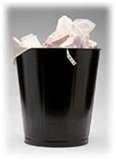
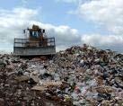
6 Sustainability 1 / 3 waste is paper of which 43% is print Newspapers 12 Packaging & other 47.7 Commercial print 7.35 Office 6.6 Standard mail m tons/yr Millions of tons/year US Paper & board disposal, 2005 US EPA Magazines 2.5 Books 1.15 Directories 0.65


7 Macro-Trends Are Helping to Drive Electronic Paper Mobile Internet Clean Technology Printed Electronics Digital Media *courtesy of Mike McCreary, E Ink


8 Electronic Publishing is a Multi-$B Addressable Market $100B- $300B annual publishing industry today, about the same as the whole current display industry* Mobile electronic books have not previously succeeded because they lacked the attributes of paper: low cost, outdoor readability, light weight (low power), &mechanical toughness. A library in your hands *courtesy of Mike McCreary, E Ink


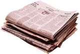
9 Newspapers Need an Alternative to Paper Paper newspaper subscriptions are dropping sharply 12 hour delay in receiving news newest generations of people are on-line much more increased sensitivity to ecology issues Newspaper profitability is under pressure as a result increasing energy costs On-line subscriptions are growing but it takes on-line subscribers to make up for one lost paper subscription* Digital distribution enables personalization Geographic localization enhanced Individually targeted content and advertising A paper-like reader appliance is needed Low cost, portable, daylight readable, mechanically tough *courtesy of Mike McCreary, E Ink


10 Paper Newspapers and the Environment OIL OIL OIL OIL OIL OIL OIL OIL OIL OIL OIL OIL 1/5 ton per subscription per year *courtesy of Mike McCreary, E Ink

11 Economic Reasons to Move From Paper Newspapers Printing $6.7M Building, G&A $27.6M Advertising $7.3M Newroom $9.9M Circulation $10.1M Ink and paper $10.4M Composite Newspaper Business Profile* 100,000 Circulation $83.9M Revenue $72.1M Total Cost ~10% Profit Newspapers could eliminate $27M (~38%) from its variable budget by moving away from printed newspapers But it will be critical to keep subscriptions and advertising rates high with electronic newspapers *Published by Bill Richards (former NY Times and Washington Post reporter) *courtesy of Mike McCreary, E Ink
12 Outline Introduction What are the key attributes of a paper-like display Why we need paper-like displays High Performance Reflective Color Self-Aligned Imprint Lithography (SAIL) Benefits and challenges of roll-to-roll (R2R) manufacturing SAIL basics green manufacturing for green products toolset for 1/3m wide line world s first R2R active matrix displays ZXO based TFTs for enhanced performance

 400 500 600 700 [nm] R+G+B =")
13 Architectures to address full color gamut additive side-by-side subpixels stacked layers additive subtractive max.=33% R+G+B = grey (dim) [nm] R+G+B = murky white [nm] -R -G -B = brown (so add black)
14 Why is it hard? Uncontrolled ambient light in - direction, color, Perfectly diffuse light out 3 or 4 electrodes sets per pixel Millions of pixels All have to work Optical management -very low loss (materials, processes, architecture) x (optical, electrical, cost) = Systems approach is essential If 13 interfaces present with each 98% efficient then max roundtrip reflectivity ~60%
15 Use of color selective mirrors can increase reflectivity by 20% compared to basic stacked design Blue mirror Green mirror Red (All) mirror

16 Brightness /contrast progress ΔL* (white black) Target region Newsprint/ SNAP Low DR -ve, no inters High DR +ve, rough resist, optimised gaps High DR +ve, rough resist Low DR -ve, rough resist High DR -ve, rough resist High DR +ve, luminit High DR +ve, Luminit, static High DR +ve, rough resist, optimised gaps, narrow illumination E-ink measured + perfect RGBW filter model low DR -ve plastic, luminit low DR -ve plastic, luminit, narrow illumination L* white state

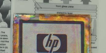
17 HP Labs Reflective Color Demonstrator

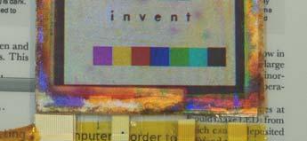
18 Color demonstrator video
19 Outline Introduction What are the key attributes of a paper-like display Why we need paper-like displays High Performance Reflective Color Self-Aligned Imprint Lithography (SAIL) Benefits and challenges of roll-to-roll (R2R) manufacturing SAIL basics green manufacturing for green products toolset for 1/3m wide line world s first R2R active matrix displays ZXO based TFTs for enhanced performance


20 Challenges & Benefits of R2R Electronics Fabrication Benefits Challenges Lower substrate cost Steady state processing: high-throughput, high-yield Lower cleanroom requirements Cheaper equipment - better scaling? Lower process temperature Defect repair patterning Limited equipment available no previous generation
21 Imprint Lithography is the Best Choice for R2R Patterning Photolithography Imprint lithography Inkjet Physical mask Laser ablation Throughput Moderate: limited by step & repeat / stitching High: > 5 meters/min Low Limited only by deposition Low Resolution Limited by substrate flatness ~10μ 100nm demonstrated >10μ 10μ -100μ ~10μ Alignment Limited by substrate flatness ~10μ Self alignment possible External sensor required poor ~10μ Issues Scaling to large areas costly New technology Materials must be jettable Cleaning, particles Thermal effects, selectivity


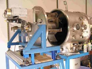
22 SAIL (Self-Aligned Imprint Lithography): Process flow is radically different from conventional flat-panel / integrated circuit fabrication deposition imprint etch Vacuum deposition of metals, dielectrics, & semiconductors Multiple mask levels imprinted as single 3D structure Patterning completed w/ wet & dry processes 5μ Conventional Photo-Lith SAIL deposit deposit imprint etch strip/clean spin resist etch develop align/expose etch mask


23 Phicot s parent PowerFilm Solar is the first and only company to manufacture a-si solar cells on plastic with a R2R process


24 Basic Imprint Lithography Process 1: coated substrate 2: coat with polymer 3: emboss 1μm Pixel speed depends linearly on mobility but inversely with the square of channel length t pixel μ ( V 2 L 2 G V T ) 4: cure with UV ~40nm lines on 50μ polyimide 5: release 6: etch μm 4 levels in 0.5 μ step heights 1 0 Multilevel structures on flex at 5m/min


25 SAIL: Self-Aligned Imprint Lithography Photolithography Multiple masking and alignment steps required Different mask used to pattern each layer Process induced distortion of 200ppm results in 20μ misalignment over 10cm SAIL SAIL encodes multiple patterns and alignments into thickness modulations of a monolithic masking structure Single mask used to pattern all the layers multiple times No misalignment because mask distorts with substrate
 to to define substrate of area channel")
26 SAIL backplane: patterning process flow Imprint Etch Disassemble Then Remove Next Etch top remove polymer exposed through mask the metal remaining polymer on array contact and a top stack TFT second one Finally remove gate all stack contact semiconductor polymer layer the time metal down way at consisting layer a and expose time the expose (optionally) to to define substrate of area channel expose the dielectric to expose gate Top TFT structure. gate completed semiconductor undercutting covering other layers channel metal dielectric layers covering Begin TFT backplane the channel by form bottom the lines that were isolated Contact removing metal crossovers gate lines layer the top thin metal by the undercut (optional) regions Semiconductor isolate the gate lines Dielectric and the TFTs Bottom metal Process produces complete backplane: TFT Pixel electrode Data line Crossover Gate line
27 SAIL solves alignment problem & saves money Multiple photoresist applications dominate photolithography process materials costs cost per ft 2 Backplane materials costs for R2R photolith & SAIL $18.00 $16.00 $14.00 $12.00 $10.00 $8.00 $6.00 $4.00 $2.00 $0.00 Photolithography Cost of Patterning SAIL R2R SAIL R2R photolith (AGI) Web cost Strip-off 2P RIE etch oxide Under-cut Al (1-3 um) RIE etch n+ Wet etch Cr Thin down 2P (clear gate-pad) RIE etch n+&si&sin Pre-Cr-etch Cleaning Thin down 2P (clear gate-pad) Plasma etch Al RIE etch oxide RIE etch n+&si&sin Wet etch Cr Imprint SAIL structure SD metal deposition (Cr) PECVD oxide/nitride/si/n+ deposition Gate metal deposition (Al) Condition web (de-hydro) Web cost Align and Expose Sputter Dep Interconnect Align and Expose Sputter Dep/ ITO Align and Expose Ultrasonic Clean Si RIE & Resist Strip Align and Expose SiN, a-si, N+ dep Align and Expose Sputter Gate 1 Metal Web preparation $0.0 $0.5 $1.0 $1.5 $2.0 $2.5 $0.0 $0.5 $1.0 $1.5 $2.0 $2.5 $3.0
28 Outline Introduction What are the key attributes of a paper-like display Why we need paper-like displays High Performance Reflective Color Self-Aligned Imprint Lithography (SAIL) Benefits and challenges of roll-to-roll (R2R) manufacturing SAIL basics green manufacturing for green products toolset for 1/3m wide line world s first R2R active matrix displays ZXO based TFTs for enhanced performance
29 Green manufacturing for a green product Less is better: 50μm thick plastic vs. 0.7mm thick glass Less process materials: removal of photolith reduces process consumables Energy costs: transients involved in batch consume energy; steady state is more efficient Reduced clean room requirements: Smaller equipment footprint
30 The web rolled on the core is its own clean room HEPA filter Ambient Process Vacuum Process

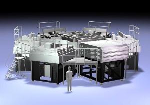
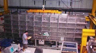
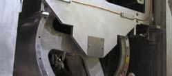
31 Equipment footprint comparison between R2R and flat panel 330mm imprint system Gen10 cluster tool
32 Patterning scaling: R2R imprinter compared to panel stepper comparison made at equal throughput equipment cost scaling comparison: panel stepper vs R2R imprinter 10 0 equipment cost [M$] / throughput [cm 2 / S] mm R2R imprinter 330 mm R2R imprinter generation Scaling similar for R2R and panel; cost much lower for R2R
33 PECVD Scaling: R2R photovoltaic compared to panel comparison made at equal throughput equipment cost [M$] / throughput [cm 2 / S] equipment cost scaling comparison: panel CVD vs R2R CVD 330 mm R2R PECVD 1 m R2R PECVD generation Again; scaling similar for R2R and panel; cost much lower for R2R
34 Outline Introduction What are the key attributes of a paper-like display Why we need paper-like displays High Performance Reflective Color Self-Aligned Imprint Lithography (SAIL) Benefits and challenges of roll-to-roll (R2R) manufacturing SAIL basics green manufacturing for green products toolset for 1/3m wide line world s first R2R active matrix displays ZXO based TFTs for enhanced performance

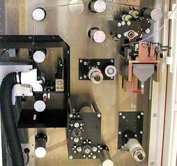
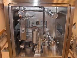
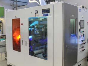

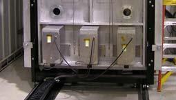
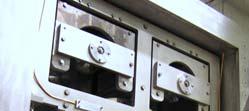
35 13 production solar cell deposition R2R Tool Development 13 drum PECVD 13 drum RIE 13 wet etcher 4 imprinter 13 drum sputter 13 RIE 10 drum PECVD 13 imprinter


36 Web based tools are a lot simpler to build than big panel tools
37 Outline Introduction What are the key attributes of a paper-like display Why we need paper-like displays High Performance Reflective Color Self-Aligned Imprint Lithography (SAIL) Benefits and challenges of roll-to-roll (R2R) manufacturing SAIL basics green manufacturing for green products toolset for 1/3m wide line world s first R2R active matrix displays ZXO based TFTs for enhanced performance
38 Performance of Full-SAIL a-si TFTs Full SAIL TFTs with thinner dielectrics have greatly improved performance on-off ratio > μA on-current mobility from linear portion of transfer curve as high as 0.8 cm 2 /V/S near linear scaling of I on vs 1/L to L~2μm 1.E 1 1.E-05 W=100um Vsd=10.1V Mobility [cm 2 /V/S] 1.E 0 1.E-1 1.E-2 1.E-3 1.E 0 q1 = p1 = R2= E 1 1.E 2 Channel Length [μm] Isd/(W/L) (A) 1.E-06 1.E-07 1.E-08 1.E-09 1.E-10 1.E-11 1.E-12 1.E-13 W [μm] L [μm] E Vg(V)


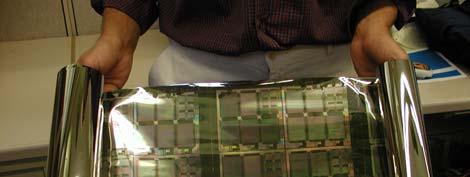
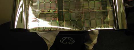
39 Initial display demonstrators SAIL Backplane on flexible substrate World s first active matrix display made exclusively with R2R processes (including E Ink Front Plane)
40 Process flow Yield Improvements: Pareto process at work Process Step Thin film deposition Imprinting Etching Device test Shunt defects Stress control Particle generation Master defects Stamp defects Imprint process Endpoint control Process design Contact liquefaction Probing errors/damage Severity 1/mm 2 unstable low low med low med med low low A bubble defect, voids are formed by insufficient volume of photopolymer to fill mold pinhole defect in metal caused by etchant diffusing through pinhole in oxide A crack defect typically results from imbalanced deposition stress Tenting defect formed by particle between stamp and substrate at imprinting time or by void in stamp Nonuniform imprinting results in premature mask erosion and feature loss Bridging caused by breakage of imprint stamp in narrow (~2u) regions
41 Outline Introduction What are the key attributes of a paper-like display Why we need paper-like displays High Performance Reflective Color Self-Aligned Imprint Lithography (SAIL) Benefits and challenges of roll-to-roll (R2R) manufacturing SAIL basics green manufacturing for green products toolset for 1/3m wide line world s first R2R active matrix displays ZXO based TFTs for enhanced performance

42 SAIL ZXO TFTs: Motivation, the 3P s Process simplification Elimination of contact layer removes 2 etch steps and one deposition step Huge increase in process margin for critical channel definition step Performance increase Even with direct metal contacts mobility is ~10X a-si at the same process temperature Higher mobility important for emissive pixels and edge electronics Pelucidity (transparency) Enable see thru displays Increase aspect ratio for conventional displays
43 SAIL ZXO TFTs: Process Simplification ZXO stack has 1 less layer then a-si Superior performance to a-si with no contact layer between top metal and semiconductor: 1 less deposition step 2 less etch steps: since all depositions performed before any etch steps some layers are etched multiple times Back-channel etch much easier to control with ZXO ZXO provides excellent etch stop for top metal etch whereas there is no etch selectivity between n+ μc-si and intrinsic a-si Embossed mask 100nm S/D metal Al 40nm N+ uc-si 30nm I-a-Si 200nm SiNx / 100nm SiOxGate dielectric 100nmGate (Al) substrate a-si stack Embossed mask W S/D metal ZXO Thermal oxide gate dielectric Substrate 6 p+ doped Si wafer Gate (Al) ZXO stack
44 SAIL ZTO TFTs: device measurements mobility for 100u long channels vs annealing temperature Transfer for W=50u, L=50u, Ta=300C 1.E E-05 1.E-06 sat incr mobility (cm^2/v/s) Ids, Ig (A) 1.E-07 1.E-08 1.E-09 1.E-10 1.E-11 Id for Vds=10V Ig 1.E temperature (C) 1.E Vg (V) Mobility strongly dependent on annealing temperature Performance unrealistically high due to high quality thermal oxide gate dielectric


45 Next steps towards commercialization September 22, 2008 PowerFilm announced that it has taken a license to the SAIL technology October 6 th, 2008 PowerFilm announced it has won a $1.4M / year cooperative agreement from the U.S. Army for development of a 'self powered flexible display'. HP Labs and PowerFilm will collaborate on the contract. PowerFilm Solar has created Phicot as a subsidiary to commercialize the technology
46 Acknowledgements The authors gratefully acknowledge the support of their collaborators and sponsors -- FlexTech Alliance - contract RFP04-112F ARL contract W911NF E Ink Corporation ASU Flexible Display Center Dupont Teijin
Defect Analysis of Roll-to-Roll SAIL Manufactured Flexible Display Backplanes
 Defect Analysis of Roll-to-Roll SAIL Manufactured Flexible Display Backplanes Carl Taussig, Richard E. Elder, Warren B. Jackson, Albert Jeans, Mehrban Jam, Ed Holland, Hao Luo, John Maltabes, Craig Perlov,
Advances in Roll-to-Roll Imprint Lithography for Display Applications Using Self Aligned Imprint Lithography. John G Maltabes HP Labs
 Advances in Roll-to-Roll Imprint Lithography for Display Applications Using Self Aligned Imprint Lithography John G Maltabes HP Labs Outline Introduction Roll to Roll Challenges and Benefits HP Labs Roll
Flexible Electronics Production Deployment on FPD Standards: Plastic Displays & Integrated Circuits. Stanislav Loboda R&D engineer
 Flexible Electronics Production Deployment on FPD Standards: Plastic Displays & Integrated Circuits Stanislav Loboda R&D engineer The world-first small-volume contract manufacturing for plastic TFT-arrays
Advanced Display Manufacturing Technology
 Advanced Display Manufacturing Technology John Busch Vice President, New Business Development Display and Flexible Technology Group September 28, 2017 Safe Harbor This presentation contains forward-looking
Scalable self-aligned active matrix IGZO TFT backplane technology and its use in flexible semi-transparent image sensors. Albert van Breemen
 Scalable self-aligned active matrix IGZO TFT backplane technology and its use in flexible semi-transparent image sensors Albert van Breemen Image sensors today 1 Dominated by silicon based technology on
AMOLED Manufacturing Process Report SAMPLE
 AMOLED Manufacturing Process Report SAMPLE 2018 AMOLED Manufacturing Process Report The report analyzes the structure and manufacturing process by dividing AMOLED into small & medium-sized rigid OLED,
PROCESS TECHNOLOGIES FOR ADVANCED ORGANIC ELECTRONIC DEVICES: MICRODISPLAYS, LIGHTING AND SOLAR CELLS
 PROCESS TECHNOLOGIES FOR ADVANCED ORGANIC ELECTRONIC DEVICES: MICRODISPLAYS, LIGHTING AND SOLAR CELLS Dr. Christian May Fraunhofer IPMS - Center for Organic Materials and Electronic Devices Dresden COMEDD
1. Publishable summary
 1. Publishable summary 1.1. Project objectives. The target of the project is to develop a highly reliable high brightness conformable low cost scalable display for demanding applications such as their
Defense Technical Information Center Compilation Part Notice
 UNCLASSIFIED Defense Technical Information Center Compilation Part Notice ADPO1 1322 TITLE: Amorphous- Silicon Thin-Film Transistor With Two-Step Exposure Process DISTRIBUTION: Approved for public release,
New Worlds for Polymers: Organic Transistors, Light Emitting Diodes, and Optical Waveguides Ed Chandross
 New Worlds for Polymers: Organic Transistors, Light Emitting Diodes, and Optical Waveguides Ed Chandross Materials Chemistry, LLC 1 Polymers in the Electronic Industry Enabling Materials Active Materials?
:: Reduce needs for heat dissipation components. :: Extend battery life in mobile products. :: Save power and reduce heat generation in TVs
 UniversalPHOLED Technology and Materials UniversalPHOLED Phosphorescent OLED technology and materials offer record-breaking performance to bring competitive advantages to your OLED display and lighting
FASwitch - A MEMS Display Backplane Manufactured by Flex Circuit Methods
 FASwitch - A MEMS Display Backplane Manufactured by Flex Circuit Methods Presenter: Dr. Nicholas F. Pasch Rolltronics Corporation 750 Menlo Ave. Menlo Park, CA 94025 npasch@rolltronics.com Introduction
Liquid Crystal Display (LCD)
") Liquid Crystal Display (LCD) When coming into contact with grooved surface in a fixed direction, liquid crystal molecules line up parallelly along the grooves. When coming into contact with grooved surface
Liquid Crystal Display (LCD) When coming into contact with grooved surface in a fixed direction, liquid crystal molecules line up parallelly along the grooves. When coming into contact with grooved surface
The Company. A leading OLED player
 The Company A leading OLED player Novaled is the company to trade with, work for and invest in. Our company focuses on proprietary organic materials and complementary innovative technologies for superior
UV Nanoimprint Tool and Process Technology. S.V. Sreenivasan December 13 th, 2007
 UV Nanoimprint Tool and Process Technology S.V. Sreenivasan December 13 th, 2007 Agenda Introduction Need tool and process technology that can address: Patterning and CD control Alignment and Overlay Defect
Pressure sensor. Surface Micromachining. Residual stress gradients. Class of clean rooms. Clean Room. Surface micromachining
 Pressure sensor Surface Micromachining Deposit sacrificial layer Si PSG By HF Poly by XeF2 Pattern anchors Deposit/pattern structural layer Etch sacrificial layer Surface micromachining Structure sacrificial
HB LEDs & OLEDs. Complete thin film process solutions
 HB LEDs & OLEDs Complete thin film process solutions Get off to a flying start for all your LED thin film deposition and etch processes From 2 inch to 8 inch Manual or fully automated substrate handling
THE challenges facing today s mobile
 MEMS displays MEMS-Based Display Technology Drives Next-Generation FPDs for Mobile Applications Today, manufacturers of mobile electronic devices are faced with a number of competitive challenges. To remain
Semiconductors Displays Semiconductor Manufacturing and Inspection Equipment Scientific Instruments
 Semiconductors Displays Semiconductor Manufacturing and Inspection Equipment Scientific Instruments Electronics 110-nm CMOS ASIC HDL4P Series with High-speed I/O Interfaces Hitachi has released the high-performance
projectors, head mounted displays in virtual or augmented reality use, electronic viewfinders
 Beatrice Beyer Figure 1. (OLED) microdisplay with a screen diagonal of 16 mm. Figure 2. CMOS cross section with OLED on top. Usually as small as fingernails, but of very high resolution Optical system
Leveraging 300 mm Technology Solutions to Enable New MEMS Process Capabilities
 Leveraging 300 mm Technology Solutions to Enable New MEMS Process Capabilities Evan Patton Semicon Europa November 2017 Lam Research Corp. 1 Presentation Outline The Internet of Things (IoT) as a market
FLEX2017 June, Monterey, USA Dr Mike Cowin, CMO, SmartKem.
 FLEX2017 June, Monterey, USA Dr Mike Cowin, CMO, SmartKem. FLEX2017 June, Monterey, USA Dr Mike Cowin, CMO, SmartKem. EU H2020 FLEXTRANs Grant Objectives A 24 month project (started September 2016) (Grant
AIXTRON in EXCILIGHT project
 AIXTRON SE AIXTRON in EXCILIGHT project Gintautas Simkus ABOUT AIXTRON 2 Who we are Headquarter based in Herzogenrath, Germany Worldwide presence with 14 sales/representatives offices and production facilities
DARPATech 99 DARPA/MTO. Bruce Gnade
 DARPATech 99 DARPA/MTO Bruce Gnade High Definition Systems Objective: Develop leading-edge display technology to meet diverse, but specific, DoD needs. The goals include increased power efficiency, reduced
Wafer Thinning and Thru-Silicon Vias
 Wafer Thinning and Thru-Silicon Vias The Path to Wafer Level Packaging jreche@trusi.com Summary A new dry etching technology Atmospheric Downstream Plasma (ADP) Etch Applications to Packaging Wafer Thinning
P I SCALE Creating an Open Access Flexible O L E D P ilo t L in e S e r vic e
 P I SCALE Creating an Open Access Flexible O L E D P ilo t L in e S e r vic e Pavel Kudlacek pavel.kudlacek@tno.nl P I - SCALE for 2017Flex 1 Lighting c h a lle n g e L ig h t in g c h a lle n g e At least
Thin-Film Encapsulation of Organic Light Emitting Devices (OLEDs) Dr. Emilie Galand Huntsman Advanced Materials CSEM Plastic Optoelectronics - Basel
 Dr. Emilie Galand Huntsman Advanced Materials CSEM Plastic Optoelectronics - Basel") Thin-Film Encapsulation of Organic Light Emitting Devices (OLEDs) Dr. Emilie Galand CSEM Plastic Optoelectronics - Basel 25th June 2010 About Huntsman Huntsman is a global manufacturer and marketer of
Thin-Film Encapsulation of Organic Light Emitting Devices (OLEDs) Dr. Emilie Galand CSEM Plastic Optoelectronics - Basel 25th June 2010 About Huntsman Huntsman is a global manufacturer and marketer of
OLED Status quo and our position
 OLED Status quo and our position Information Day 2013 A Deep Dive into the LC&OLED Business Dr. Udo Heider Vice President OLED Darmstadt, Germany June 26, 2013 Disclaimer Remarks All comparative figures
[1.9] AMOLED 공정 Introduction OLED Materials Patterning Process Process Equipments
![[1.9] AMOLED 공정 Introduction OLED Materials Patterning Process Process Equipments](/thumbs/73/69073032.jpg "[1.9] AMOLED 공정 Introduction OLED Materials Patterning Process Process Equipments") [1.9] AMOLED 공정 1.9.1. Introduction 1.9.2. OLED Materials 1.9.3. Patterning Process 1.9.4. Process Equipments OLED : Organic Light Emitting Diode Organic EL : Organic Electroluminescent 재료및공정 재료의발광메카니즘
[1.9] AMOLED 공정 1.9.1. Introduction 1.9.2. OLED Materials 1.9.3. Patterning Process 1.9.4. Process Equipments OLED : Organic Light Emitting Diode Organic EL : Organic Electroluminescent 재료및공정 재료의발광메카니즘
Nano-Imprint Lithography Infrastructure: Imprint Templates
 Nano-Imprint Lithography Infrastructure: Imprint Templates John Maltabes Photronics, Inc Austin, TX 1 Questions to keep in mind Imprint template manufacturability Resolution Can you get sub30nm images?
Technology White Paper Plasma Displays. NEC Technologies Visual Systems Division
 Technology White Paper Plasma Displays NEC Technologies Visual Systems Division May 1998 1 What is a Color Plasma Display Panel? The term Plasma refers to a flat panel display technology that utilizes
Phosphorescent OLED Technologies: The Next Wave. Plastic Electronics Conference Oct 9, 2012
 Phosphorescent OLED Technologies: The Next Wave Plastic Electronics Conference Oct 9, 2012 UDC Company Focus IP innovator, technology developer, patent licensor and materials supplier for the rapidly growing
Self-Aligned Double Patterning for 3xnm Flash Production
 Self-Aligned Double Patterning for 3xnm Flash Production Chris Ngai Dir of Process Engineering & Lithography Maydan Technology Center Group Applied Materials, Inc. July 16 th, 2008 Overview Double Patterning
Display Technologies. Corning: The Technology Behind the Glass
 Display Technologies Corning: The Technology Behind the Glass Dr. David Chen Director, Application Engineering and Asia Commercial Technology Taiwan Corning Display Technologies Taiwan June 13, 2008 Forward
Applied Materials. 200mm Tools & Process Capabilities For Next Generation MEMS. Dr Michel (Mike) Rosa
 Rosa") Applied Materials 200mm Tools & Process Capabilities For Next Generation MEMS Dr Michel (Mike) Rosa 200mm MEMS Global Product / Marketing Manager, Components and Systems Group (CSG), Applied Global Services
Applied Materials 200mm Tools & Process Capabilities For Next Generation MEMS Dr Michel (Mike) Rosa 200mm MEMS Global Product / Marketing Manager, Components and Systems Group (CSG), Applied Global Services
TipatOr. Liquid metal switch (LMS) display technology. Avi Fogel
 display technology. Avi Fogel") TipatOr Liquid metal switch (LMS) display technology Avi Fogel 972-52-5702938 avifog@gmail.com Who is behind TipatOr TipatOr emerged from a merger of 2 expert groups in the fields of MEMS and Displays
TipatOr Liquid metal switch (LMS) display technology Avi Fogel 972-52-5702938 avifog@gmail.com Who is behind TipatOr TipatOr emerged from a merger of 2 expert groups in the fields of MEMS and Displays
An Overview of OLED Display Technology
 page:1 An Overview of OLED Display Technology Homer Antoniadis OSRAM Opto Semiconductors Inc. San Jose, CA page:2 Outline! OLED device structure and operation! OLED materials (polymers and small molecules)!
Digital Light Processing
 A Seminar report On Digital Light Processing Submitted in partial fulfillment of the requirement for the award of degree of Bachelor of Technology in Computer Science SUBMITTED TO: www.studymafia.org SUBMITTED
Reduction of Device Damage During Dry Etching of Advanced MMIC Devices Using Optical Emission Spectroscopy
 Reduction of Device Damage During Dry Etching of Advanced MMIC Devices Using Optical Emission Spectroscopy D. Johnson, R. Westerman, M. DeVre, Y. Lee, J. Sasserath Unaxis USA, Inc. 10050 16 th Street North
R2R Processing of Flexible Devices
 R2R Processing of Flexible Devices Mani Thothadri, PhD Senior Director, New Business & Strategic Initiatives Display & Flexible Technologies Group Flextech June 20, 2017 Acknowledgements Dan Forster Christoph
ID C10C: Flat Panel Display Basics
 ID C10C: Flat Panel Display Basics Renesas Electronics America Inc. Robert Dunhouse, Display BU Engineering Manager 12 October 2010 Revision 1.1 Robert F. Dunhouse, Jr. Displays Applications Engineering
Screens; media that use additive primaries
 Image display Display is the final stage in the image processing pipeline: Continuous scenes are acquired and digitally processed. The display process essentially converts the discrete image back to continuous
Overcoming Challenges in 3D NAND Volume Manufacturing
 Overcoming Challenges in 3D NAND Volume Manufacturing Thorsten Lill Vice President, Etch Emerging Technologies and Systems Flash Memory Summit 2017, Santa Clara 2017 Lam Research Corp. Flash Memory Summit
Next Generation of Poly-Si TFT Technology: Material Improvements and Novel Device Architectures for System-On-Panel (SOP)
") Next Generation of Poly-Si TFT Technology: Material Improvements and Novel Device Architectures for System-On-Panel (SOP) Tolis Voutsas* Paul Schuele* Bert Crowder* Pooran Joshi* Robert Sposili* Hidayat
Next Generation of Poly-Si TFT Technology: Material Improvements and Novel Device Architectures for System-On-Panel (SOP) Tolis Voutsas* Paul Schuele* Bert Crowder* Pooran Joshi* Robert Sposili* Hidayat
Principles of Electrostatic Chucks 6 Rf Chuck Edge Design
 Principles of Electrostatic Chucks 6 Rf Chuck Edge Design Overview This document addresses the following chuck edge design issues: Device yield through system uniformity and particle reduction; System
 Page 1 of 8 Main > Electronics > Computers How OLEDs Work by Craig Freudenrich, Ph.D. Introduction to How OLEDs Work Imagine having a high-definition TV that is 80 inches wide and less than a quarter-inch
Defect Reduction for Semiconductor Memory Applications Using Jet And Flash Imprint Lithography
 Defect Reduction for Semiconductor Memory Applications Using Jet And Flash Imprint Lithography Zhengmao Ye, Kang Luo, Xiaoming Lu, Brian Fletcher, Weijun Liu, Frank Xu, Dwayne LaBrake, Douglas Resnick,
MicroLED Displays: Global Trends & Opportunities for Equipment and Material Suppliers
 Picture: Sony From Technologies to Market MicroLED Displays: Global Trends & Opportunities for Equipment and Material Suppliers SEMICON EUROPA Jean-Christophe ELOY - CEO - Yole Développement 2017 AGENDA
Organic light emitting diode (OLED) displays
 displays") Ultra-Short Pulse Lasers Enable Precision Flexible OLED Cutting FLORENT THIBAULT, PRODUCT LINE MANAGER, HATIM HALOUI, APPLICATION MANAGER, JORIS VAN NUNEN, PRODUCT MARKETING MANAGER, INDUSTRIAL PICOSECOND
Ultra-Short Pulse Lasers Enable Precision Flexible OLED Cutting FLORENT THIBAULT, PRODUCT LINE MANAGER, HATIM HALOUI, APPLICATION MANAGER, JORIS VAN NUNEN, PRODUCT MARKETING MANAGER, INDUSTRIAL PICOSECOND
SEMICONDUCTOR TECHNOLOGY -CMOS-
 SEMICONDUCTOR TECHNOLOGY -CMOS- Fire Tom Wada What is semiconductor and LSIs Huge number of transistors can be integrated in a small Si chip. The size of the chip is roughly the size of nails. Currently,
Flat Panel Displays: LCD Technologies and Trends
 Flat Panel Displays: LCD Technologies and Trends Robert Dunhouse, Sr. Engineering Manager, Display BU Class ID: 4C01B Renesas Electronics America Inc. Robert F. Dunhouse, Jr. Sr. Engineering Manager, Display
SEMICONDUCTOR TECHNOLOGY -CMOS-
 SEMICONDUCTOR TECHNOLOGY -CMOS- Fire Tom Wada 2011/12/19 1 What is semiconductor and LSIs Huge number of transistors can be integrated in a small Si chip. The size of the chip is roughly the size of nails.
Solid State Devices 4B6
 Solid State Devices 4B6 Lecture 13 Projection and 3D displays: LCD, DLP and LCOS Daping Chu Lent 2016 Development of flat panel displays (FPDs) (LCD) in early days 1 A 105 inch TFT-LCD 4k2k curved panel
Challenges in the design of a RGB LED display for indoor applications
 Synthetic Metals 122 (2001) 215±219 Challenges in the design of a RGB LED display for indoor applications Francis Nguyen * Osram Opto Semiconductors, In neon Technologies Corporation, 19000, Homestead
IOSR Journal of Engineering (IOSRJEN) ISSN (e): , ISSN (p): Volume 2, PP Organic Led. Figure 1.
 ISSN (e): , ISSN (p): Volume 2, PP Organic Led. Figure 1.") IOSR Journal of Engineering (IOSRJEN) ISSN (e): 2250-3021, ISSN (p): 2278-8719 Volume 2, PP 46-51 www.iosrjen.org Organic Led Prof.Manoj Mishra 1, Sweety Vade 2,Shrutika Sawant 3, Shriwari Shedge 4, Ketaki
IOSR Journal of Engineering (IOSRJEN) ISSN (e): 2250-3021, ISSN (p): 2278-8719 Volume 2, PP 46-51 www.iosrjen.org Organic Led Prof.Manoj Mishra 1, Sweety Vade 2,Shrutika Sawant 3, Shriwari Shedge 4, Ketaki
Overview of All Pixel Circuits for Active Matrix Organic Light Emitting Diode (AMOLED)
") Chapter 2 Overview of All Pixel Circuits for Active Matrix Organic Light Emitting Diode (AMOLED) ---------------------------------------------------------------------------------------------------------------
Chapter 2 Overview of All Pixel Circuits for Active Matrix Organic Light Emitting Diode (AMOLED) ---------------------------------------------------------------------------------------------------------------
These are used for producing a narrow and sharply focus beam of electrons.
 CATHOD RAY TUBE (CRT) A CRT is an electronic tube designed to display electrical data. The basic CRT consists of four major components. 1. Electron Gun 2. Focussing & Accelerating Anodes 3. Horizontal
Advanced WLP Platform for High-Performance MEMS. Presented by Dean Spicer, Director of Engineering
 Advanced WLP Platform for High-Performance MEMS Presented by Dean Spicer, Director of Engineering 1 May 11 th, 2016 1 Outline 1. Application Drivers for High Performance MEMS Sensors 2. Approaches to Achieving
Joint Development of Ultra-Bright, Inorganic EL Light-Emitting Materials. November 2, 2005 KURARAY CO., LTD.
 Joint Development of Ultra-Bright, Inorganic EL Light-Emitting Materials November 2, 2005 KURARAY CO., LTD. Sales Trends of Display-related Products (Kuraray (standalone)) FY1994 FY1999 FY2004 Sales Ratio
Design of Organic TFT Pixel Electrode Circuit for Active-Matrix OLED Displays
 JOURNAL OF COMPUTERS, VOL. 3, NO. 3, MARCH 2008 1 Design of Organic TFT Pixel Electrode Circuit for Active-Matrix Displays Aram Shin, Sang Jun Hwang, Seung Woo Yu, and Man Young Sung 1) Semiconductor and
P-224: Damage-Free Cathode Coating Process for OLEDs
 P-224: Damage-Free Cathode Coating Process for OLEDs Shiva Prakash DuPont Displays, 6 Ward Drive, Santa Barbara, CA 937, USA Abstract OLED displays require the growth of inorganic films over organic films.
The future of microled displays using nextgeneration
 The future of microled displays using nextgeneration technologies Introduction MicroLEDs (micro-light-emitting diodes) are an emerging display technology that, as the name implies, use very small LEDs
LEP400 Etch Depth Monitor Real-time, in-situ plasma etch depth monitoring and end point control plus co-linear wafer vision system
 LEP400 Etch Depth Monitor Real-time, in-situ plasma etch depth monitoring and end point control plus co-linear wafer vision system Base Configuration Etch Depth Monitoring LEP400 Recessed Window Plasma
the Most Popular Display Technology?
 Why is LCD the Most Popular Display Technology? History of Liquid Crystal Display (LCD) As early as 1889, scientists discovered that chemicals such as cholesteryl benzoate, when melted into liquid form,
Perfecting the Package Bare and Overmolded Stacked Dies. Understanding Ultrasonic Technology for Advanced Package Inspection. A Sonix White Paper
 Perfecting the Package Bare and Overmolded Stacked Dies Understanding Ultrasonic Technology for Advanced Package Inspection A Sonix White Paper Perfecting the Package Bare and Overmolded Stacked Dies Understanding
Technology Overview LTCC
 Sheet Code RFi0604 Technology Overview LTCC Low Temperature Co-fired Ceramic (LTCC) is a multilayer ceramic substrate technology that allows the realisation of multiple embedded passive components (Rs,
High aspect ratio deep RIE for novel 3D radiation sensors in high energy physics applications
 High aspect ratio deep RIE for novel 3D radiation sensors in high energy physics applications Angela Kok, Thor-Erik Hansen, Trond Hansen, Geir Uri Jensen, Nicolas Lietaer, Michal Mielnik, Preben Storås
VARIOUS DISPLAY TECHNOLOGIESS
 VARIOUS DISPLAY TECHNOLOGIESS Mr. Virat C. Gandhi 1 1 Computer Department, C. U. Shah Technical Institute of Diploma Studies Abstract A lot has been invented from the past till now in regards with the
Sep 09, APPLICATION NOTE 1193 Electronic Displays Comparison
 Sep 09, 2002 APPLICATION NOTE 1193 Electronic s Comparison Abstract: This note compares advantages and disadvantages of Cathode Ray Tubes, Electro-Luminescent, Flip- Dot, Incandescent Light Bulbs, Liquid
SPATIAL LIGHT MODULATORS
 SPATIAL LIGHT MODULATORS Reflective XY Series Phase and Amplitude 512x512 A spatial light modulator (SLM) is an electrically programmable device that modulates light according to a fixed spatial (pixel)
High ResolutionCross Strip Anodes for Photon Counting detectors
 High ResolutionCross Strip Anodes for Photon Counting detectors Oswald H.W. Siegmund, Anton S. Tremsin, Robert Abiad, J. Hull and John V. Vallerga Space Sciences Laboratory University of California Berkeley,
Multilevel Beam SOI-MEMS for Optical Applications
 pp. 281-285 Multilevel Beam SOI-MEMS for Optical Applications Veljko Milanović Adriatic Research Institute 2131 University Ave., Suite 322, Berkeley, CA 94704 veljko@adriaticresearch.org Abstract A microfabrication
Industrial Inline Control for Advanced Vacuum Roll to Roll Systems. Gerhard Steiniger Web inspection - surface Quallity control 7.
 Industrial Inline Control for Advanced Vacuum Roll to Roll Systems Gerhard Steiniger Web inspection - surface Quallity control 7.4-7684 1 Industrial Inline Control for Advanced Vacuum Roll to Roll Systems
Illumination Challenges in Non- Industrial Vision Applications. Simon Stanley Managing Director ProPhotonix IRL Ltd
 Illumination Challenges in Non- Industrial Vision Applications Simon Stanley Managing Director ProPhotonix IRL Ltd ProPhotonix designs and manufactures high-quality LED systems and laser modules for the
Development of OLED Lighting Applications Using Phosphorescent Emission System
 Development of OLED Lighting Applications Using Phosphorescent Emission System Kazuhiro Oikawa R&D Department OLED Lighting Business Center KONICA MINOLTA ADVANCED LAYERS, INC. October 10, 2012 Outline
Basically we are fooling our brains into seeing still images at a fast enough rate so that we think its a moving image.
 Basically we are fooling our brains into seeing still images at a fast enough rate so that we think its a moving image. The formal definition of a Moving Picture... A sequence of consecutive photographic
 Chapter 3 Evaluated Results of Conventional Pixel Circuit, Other Compensation Circuits and Proposed Pixel Circuits for Active Matrix Organic Light Emitting Diodes (AMOLEDs) -------------------------------------------------------------------------------------------------------
PUBLISHABLE Summary To provide OLED stacks with improved reliability Provide improved thin film encapsulation
 PUBLISHABLE Summary SCOOP is a European funded project (FP7 project number 287595 SCOOP). It is focused on OLED technology, microdisplays based on the combination of OLED with CMOS technology, and innovative
Organic light emitting diodes for display technology
 Organic light emitting diodes for display technology Shamna Shamsudeen MScTI - ZITI-Heidelberg University OLED ZITI, Uni Heidelberg Page1 What s Light Light: Visible part of EM spectra. Ref:[1] Thermoluminescence:
MEMS Technologies Dresden - Product Development and Fabrication at IPMS Dresden
 MEMS Technologies Dresden - Product Development and Fabrication at IPMS Dresden MEMS Technologies Dresden - Product Development and Fabrication at IPMS Dresden Michael Müller, Matthias List Outline FhG-IPMS
Defense Technical Information Center Compilation Part Notice
 UNCLASSIFIED Defense Technical Information Center Compilation Part Notice ADPO 11305 TITLE: Advanced Manufacturing Technologies on Color Plasma Displays DISTRIBUTION: Approved for public release, distribution
ADDING AN O TO LEDS STATUS AND PERSPECTIVES OF ORGANIC LIGHT EMITTING DIODES PAWEL E. MALINOWSKI, TUNGHUEI KE LED EVENT 2017
 ADDING AN O TO LEDS STATUS AND PERSPECTIVES OF ORGANIC LIGHT EMITTING DIODES PAWEL E. MALINOWSKI, TUNGHUEI KE LIVING ROOM NOT SO LONG AGO... 2 Source: Warner Bros. Incadescent CRT 3 Source: Warner Bros.
Readiness and Challenges of EUV Mask
 Panel Discussion: EUVL HVM Insertion and Scaling Readiness and Challenges of EUV Mask Takashi Kamo Toshiba Corporation Semiconductor & Storage Products Company Contents [1] Introduction [2] EUV Mask Defect
EQUIPMENT COATING SYSTEMS FOR THIN-FILM PV THIN-FILM PHOTOVOLTAICS. SCALA VISS PIA nova GC120VCR XENIA
 THIN-FILM PHOTOVOLTAICS EQUIPMENT COATING SYSTEMS FOR THIN-FILM PV SCALA VISS PIA nova GC120VCR XENIA OUR STORY. OUR EXPERIENCE. RANGE OF APPLICATIONS VON ARDENNE provides advanced PVD coating equipment
ORGANIC ELECTRONICS PROCESS DEVELOPMENT AND ENCAPSULATION TECHNOLOGIES
 FRAUNHOFER INSTITUTE FOR ORGANIC ELECTRONICS, ELECTRON BEAM AND PLASMA TECHNOLOGY FEP ORGANIC ELECTRONICS PROCESS DEVELOPMENT AND ENCAPSULATION TECHNOLOGIES 2 PROFILE Fraunhofer FEP combines research and
EQUIPMENT VACUUM WEB COATING SYSTEMS ROLL-TO-ROLL ROLL-TO-ROLL
 ROLL-TO-ROLL EQUIPMENT VACUUM WEB COATING SYSTEMS ROLL-TO-ROLL VACUUM WEB COATING APPLICATIONS VON ARDENNE provides tailored web coating solutions for today s most ambitious thin-film applications on polymer
SNU PRECISION CO., LTD
 SNU PRECISION CO., LTD 1629-2 Nakseongdae-dong, Kwanak-ku in Seoul, SOUTH KOREA The First Quarter 2011 Disclaimer This document has been prepared by SNU Precision CO., Ltd.( the Company ). Until 2010,
Performance Comparison of Bilayer and Multilayer OLED
 Performance Comparison of Bilayer and Multilayer OLED Akanksha Uniyal, Poornima Mittal * Department of Electronics and Communication School of Engineering and Technology Graphic Era University, Dehradun-248002,
SUPPLEMENTARY INFORMATION
 User-interactive electronic-skin for instantaneous pressure visualization Chuan Wang 1,2,3, David Hwang 1,2,3, Zhibin Yu 1,2,3, Kuniharu Takei 1,2,3, Junwoo Park 4, Teresa Chen 4, Biwu Ma 3,4, and Ali
The Flat Panel Display Paradigm: Successful Implementation of Microelectronic Processes on Gigantic Wafers
 The Flat Panel Display Paradigm: Successful Implementation of Microelectronic Processes on Gigantic Wafers Dr. Zvi Yaniv Applied Nanotech, Inc. 3006 Longhorn Blvd., Suite 107 Austin, TX 78758 Phone 512-339-5020
mirasol Display Value Proposition White Paper
 VALUEPROPOSI TI ON mi r asoldi spl ays Whi t epaper I June2009 Table of Contents Introduction... 1 Operational Principles... 2 The Cellular Phone Energy Gap... 3 Energy Metrics... 4 Energy Based Advantages...
Application note. Materials. Introduction. Authors. Travis Burt, Huang ChuanXu*, Andy Jiang* Agilent Technologies Mulgrave, Victoria, Australia
 Performance of compact visual displays measuring angular reflectance of optically active materials using the Agilent Cary 7000 Universal Measurement Spectrophotometer (UMS) Application note Materials Authors
A NOVEL METHOD FOR TESTING LCD BY INTEGRATING SHORTING BAR AND TAGUCHI DOE TECHNOLOGIES
 This article has been peer reviewed and accepted for publication in JMST but has not yet been copyediting, typesetting, pagination and proofreading process. Please note that the publication version of
Deep Silicon Etch Technology for Advanced MEMS Applications
 Deep Silicon Etch Technology for Advanced MEMS Applications Shenjian Liu, Ph.D. Managing Director, AMEC AMEC Company Profile and Product Line-up AMEC HQ, R&D and MF Facility in Shanghai AMEC Taiwan AMEC
Present and future of OLED lighting
 Present and future of OLED lighting Dr. Wolfgang Dötter Authorized Company Officer OLEDWorks Global Q-EHS Manager & Senior Integral Project Manager 1 Vision In 10 years there will be only Solid State Lighting;
Solution-based transistor matrix
 18 PRINTED ELECTRONICS Solution-based transistor matrix A groundbreaking new technology is making it far more cost-effective to produce the electronic control unit of liquid crystal displays. At the same
ADVANCEMENTS IN GRAVURE TECHNOLOGY: FOR SUSTAINABILITY AND GROWTH PRINTED LIGHTING TECHNOLOGY
 ADVANCEMENTS IN GRAVURE TECHNOLOGY: FOR SUSTAINABILITY AND GROWTH PRINTED LIGHTING TECHNOLOGY Marc Chason Marc Chason and Associates, Inc. marcchason@sbcglobal.net January 17, 2012 Logic Driven Value Chain
Backside Circuit Edit on Full-Thickness Silicon Devices
 Backside Circuit Edit on Full-Thickness Silicon Devices Presentation Title Line 1 Title Line Two Can I really skip the global thinning step?! Date Presenter Name Chad Rue FEI Company, Hillsboro, OR, USA
Transforming Electronic Interconnect Breaking through historical boundaries Tim Olson Founder & CTO
 Transforming Electronic Interconnect Breaking through historical boundaries Tim Olson Founder & CTO Remember when? There were three distinct industries Wafer Foundries SATS EMS Semiconductor Devices Nanometers