SASTRA UNIVERSITY UNIVERSITAT POLITÈCNICA DE CATALUNYA. B. Tech. in Electronics & Communication Engineering Bachelor Thesis
|
|
|
- Stewart Bridges
- 6 years ago
- Views:
Transcription


1 1 SASTRA UNIVERSITY UNIVERSITAT POLITÈCNICA DE CATALUNYA B. Tech. in Electronics & Communication Engineering Bachelor Thesis BIT ERROR RATE TEST FOR OPTICAL COMMUNICATION LINK USING PRBS GENERATED BY AN FPGA SYSTEM DESIGN UPC Thesis Director UPC Co- Director SASTRA Mentor : Prof. José Antonio Lazaro Villa : Senior Eng. José Antonio Altabas Navarro : Prof. M.Sridharan SINDHU VAIRAVEL FEB - JUN 2014
2 2 SASTRA UNIVERSITY (A University u/s 3 of UGC Act, 1956) Thanjavur , Tamil Nadu, India School of Electrical & Electronics Engineering BONAFIDE CERTIFICATE Certified that the project work entitled BIT ERROR RATE TEST FOR OPTICAL COMMUNICATION LINK USING PRBS GENERATED BY AN FPGA SYSTEM DESIGN is the work done by SINDHU VAIRAVEL (Reg. No. : ) under my guidance in partial fulfilment for the award of the degree of Bachelor of Technology in Electronics & Communication Engineering during the period February June Prof. M. Sridharan Internal Guide / Exchange Coordinator Prof. José Antonio Lazaro Villa External Guide Senior Eng. José Antonio Altabas Navarro Supervisor Dr. K. Thenmozhi Associate Dean/ECE Dr. B. Viswanathan Dean SEEE

3 3 Prof. José Antonio Lazaro Villa Department of Signal theory and Communication, ETSETB, Universitat Politecnica de Catalunya, Barcelona, Spain CERTIFICATE This is to certify that the project work titled BIT ERROR RATE TEST FOR OPTICAL COMMUNICATION LINK USING PRBS GENERATED BY AN FPGA SYSTEM DESIGN submitted to SASTRA University by Ms. SINDHU VAIRAVEL (Reg. No.: ) in partial fulfillment of the requirements for the award of the degree of Bachelor of Technology in Electronics & Communication Engineering is the original and independent work carried out under my guidance at Department of Signal theory and Communication, ETSETB, Universitat Politecnica de Catalunya, Barcelona, Spain, during the period February to June The contents of this thesis done by her, in full, or in parts have not been submitted to any institute or University for the award of any degree or diploma. Place: Prof. José Antonio Lazaro Villa Date: Official Seal
4 4 DECLARATION I, hereby declare that the project work titled BIT ERROR RATE TEST FOR OPTICAL COMMUNICATION LINK USING PRBS GENERATED BY AN FPGA SYSTEM DESIGN submitted to SASTRA University in partial fulfillment of the requirements for the award of the degree of Bachelor of Technology in Electronics & Communication Engineering was carried out at Department of Signal theory and Communication, ETSETB, Universitat Politecnica de Catalunya, Barcelona, Spain under the guidance of Prof. José Antonio Lazaro Villa (External Guide), ETSETB, Universitat Politecnica de Catalunya, Barcelona, Spain, Prof. M. Sridharan (Internal Guide), School of Electrical & Electronics Engineering, SASTRA University, India and José Antonio Altabas Navarro (Supervisor), ETSETB, Universitat Politecnica de Catalunya, Barcelona, Spain during the academic year This was a record of my own work and to the best of my knowledge and belief, it contains no material previously published or written by another person nor material which has been accepted by any other University or Institute of higher learning, except where due acknowledgments have made in the text. Place: Date: (SINDHU VAIRAVEL)
5 5 ACKNOWLEDGEMENTS I would like to sincerely thank Prof. R. Sethuraman, Vice-Chancellor, and Dr. G. Bhalachandran, Registrar, SASTRA University for providing me an opportunity to work in such an honored Institute of International status. I also thank Dr. S. Vaidhyasubramaniam, Dean- Planning and Development and Dr. S. Swaminathan, Dean-Sponsored Research for their support and encouragement. I thank Dr. B. Viswanathan, Dean-SEEE, Associate Deans and Faculty members of SEEE, SASTRA University, for their moral support and all the faculty members who have contributed in molding me as an engineer. Thanks to Prof. José Antonio Lazaro Villa, my project guide at UPC who has been very motivating and helping me a lot during my stay at Barcelona. I would also like to thank my supervisor Senior Eng. José Antonio Altabas Navarro, ETSETB, Universitat Politecnica de Catalunya, Barcelona, Spain. I must also mention the support provided by the International Office of ETSETB, UPC, Barcelona. Very special thanks to my parents Dr. Vairavel and Dr. Kalai Selvi for the unlimited support and my brother for his encouragement throughout my life. Thanks to SASTRA University for providing an opportunity to carry out my project work at ETSETB, UPC Barcelona, Spain, through the Semester Abroad Programme and also for providing me Desh-Videsh Scholarship. Very special thanks to my Internal guide Prof. M. Sridharan, Department of Electronics & Communication Engineering, SASTRA University for his constant support for my project work/administrative procedures and for initiating and strengthening the link between SASTRA and ETSETB, UPC Barcelona, Spain. I also convey my thanks to Mr. Raja Subramanian, SAP Coordinator, Department of Training, Placements and International Relations, SASTRA University. I would also like to thank the people who answered to all my questions posted on the Altera forums.
6 6 INDEX ABSTRACT 8 1. INTRODUCTION TO OPTICAL COMMUNICATION AND ROLE OF FPGA AS AN INTERFACE Introduction Optical Fiber Communication Fiber optic communication system Need for optic-fiber Field Programmable Gate Arrays Need to use FPGAs Relevance of Cyclone III FPGA Starter Kit for this application 2. PSEUDO RANDOM BIT SEQUENCE GENERATOR & BIT ERROR RATE TESTER Overall setup PRBS generator PRBS through optical link IMPLEMENTATION: HARDWARE AND SOFTWARE Hardware Implementation Cyclone III FPGA Starter Kit THDB_ADA Daughter Board 17
7 Button Debouncing Software Implementation ModelSim Quartus II Logic Implemented EXPERIMENTAL RESULTS PRBS PRBS through optical link Transmitter_ Receiver FPGA Method Method DAC-ADC interface CONCLUSION AND FUTURE WORK Future work Challenges faced Other applications 40 REFERENCE 41 APPENDIX 43
8 8 ABSTRACT Field Programmable Gate Arrays (FPGAs) have impacted the world of communication in a way that has not only simplified complex tasks but has also made the dream of achieving fast data throughput possible. The interfacing of FPGA with optical communication system, involves the measurement of link performance by testing and properly characterizing the communication system. Bit Error Rate Testing (BERT) is an important test to study the link performance of any data transmission system. In this report, the design of a Pseudo Random Bit Sequence (PRBS) generator & BER Tester using Altera s Cyclone III FPGA Starter Kit along with Terasic s THDB_ADA daughter board is done. A PRBS generator was designed and interfaced with a single mode optical fiber to study the nature and effect of channel imperfections resulting in bit errors when information is transmitted through the fiber.
 through an optical fibre and checking for bit errors after it is received at the receiver.")
9 9 SPECIFIC OBJECTIVE One of the important steps to measure the link performance of an optical communication system is to perform Bit Error Rate Test (BERT). This involves generating and transmitting Pseudo Random Bit Sequence (PRBS) through an optical fibre and checking for bit errors after it is received at the receiver. In this thesis, Altera s Cyclone III EP3C25F324 FPGA was used as a transmitter and receiver. Pink, blue: Individual task; Green: Common task
10 10 The above work flow gives an overview of the steps carried out in the project. The three important steps as part of my contribution are described as below- Problem Statement Analysis: The characteristic behavior of a Pseudo Random Bit Sequence (PRBS) was analyzed, to generate PRBS signal using a Linear Feedback Shift Register (LFSR).The PRBS signal has to be generated at the transmitter and transmitted through a fiber optic channel. A Bit Error Rate Tester (BERT) was analyzed to be implemented at the receiver by taking into account the synchronization required between the transmitter and the receiver in order to compute bit errors.. Logic Synthesis: The logic for a Pseudorandom Bit Sequence Generator (PRBS)-Bit Error Rate Tester (BERT) was synthesized as a pseudo code. Code Synthesis: The pseudo code was then structured into a Hardware Descriptive Language (HDL), which can be processed by the resource tool (Quartus II software) to be converted into a file that is understandable by the FPGA. Code Simulation: The above code was simulated using the simulation tool ModelSim using a Testbench code to verify the logical correctness. Result analysis and correction: The results from the code simulation stage were checked for logical correctness and altered accordingly. Verification of design on the resource: Using the on-chip debugger tools available in the resource tool, namely, Quaruts II, the signals on the FPGA pins can be probed to see if it is working right, before it is verified using the complete setup.
11 11 1. INTRODUCTION TO OPTICAL COMMUNICATION AND ROLE OF FPGA AS AN INTERFACE 1.1. INTRODUCTION Life, without communication, is like a car without wheels. It is only by expressing one's thoughts and ideas with many others who have similar and new thoughts, can the dreams be realized. It is only by realizing such dreams, innovation is encouraged. Communication has not only been a key factor for various technological advancements, but has also played an important role in maintaining strong bonds within friends, family members, who live in different corners of the world. The need to transmit information at a faster rate than that is already in use is the challenge for the communication engineers. As there is so much to know so quickly, today s world demands for more advancements in the field of communication, especially in terms of speed at which information is exchanged, quality of received information and the cost effectiveness. One of the means of information exchange is by the use of light to transfer information from one point to another through a channel. This type of communication, called Optical communication, has become very popular in the recent days especially because of its massive data carrying capacity and very low post-installation maintenance cost. In communications, digital signal processing plays a major role in linking the analog world with the digital world. In order to perform high-order filtering which are essential for processing digital signal, corresponding to the real world signals, high speed processors are needed. The traditional Digital Signal Processors which are designed to perform specialized DSP application are out-weighed by Field Programmable Gate Arrays (FPGAs) when it comes to efficiency in terms power consumption, parallel processing and speed of DSP operations [1]. For communication systems which involve high speed DSP operation, the use of FPGA is the best choice as it can implement complex logic very fast OPTICAL FIBER COMMUNICATION The type of communication wherein information is transmitted from the transmitter to the receiver by modulating light that forms an electromagnetic carrier wave, in accordance to the message signal, is called optical communication. These optical pulses can be transmitted wirelessly or through wireline. Wireless transmission results in heavy loss of information due to various environmental effects which directly affect the unprotected signal. To protect the optical signal carrying important information, the optical pulses are passed through a fiber, essentially made of glass, which can transmit optical signal by total internal reflection with significantly less transmission loss. As signal is transmitted over long distances, losses do occur, for which Erbium- Doped Fiber Amplifiers (EDFA) can be used for signal regeneration.
12 FIBER OPTIC TRANSMISSION SYSTEMS A complete setup of a fiber-optic transmission system consists of three basic elements: An optical transmitter, fiber optic channel and an optical receiver. An optical transmitter gets electrical signal as input which is fed to an electro-optic modulator that modulates the signal by varying the intensity of light. The light source can be a laser or LED. The laser light is divided into two paths, by a beam splitter. One of the two paths has a phase modulator. The two paths are then recombined. By altering the electric field on the path which was phase modulated and by determining if the beams at the output interfere destructively or constructively, the intensity or amplitude of the exiting light can be controlled. This is done by a device called Mach-Zehnder modulator (MZM). The fiber-optic channel, then, acts as a medium through which the optical pulses are transmitted. The main parts of an optic fiber are: the core, which is the center of the fiber through which light is transmitted, the cladding is the region that surrounds the core in a glass and has a refractive index less than that of the core, hence allowing the light to be confined within the fiber core and an outer coating, usually made of plastic, that provides strength and protects the optical fiber from external damage. The optical receiver converts the transmitted optical pulse stream back to its corresponding electrical signal with the help of a photodetector. An electrical filter is usually used after the photodetector in order to enhance the signal quality NEED FOR OPTIC FIBER The use of optic fibers that guide light waves for communication dates back to the 1970 s. The fact that photon travels faster than electrons and, in addition can be guided similar to that of electrons, led to the use of light for achieving higher data rates at around Gb/s. This optical communication has evolved over three generations and is now available at over Tb/s data rates. These data rates have been contributed by various modern modulation techniques like the Wavelength Division Multiplexing (WDM). Also, hardware tools like the Field Programmable Gate Arrays that provide parallel, embedded Digital Signal Processing solutions facilitate an additional ease with achieving such high rates. The data-handling capability of Optical fibers exceeds that of copper wire with respect to many factors like, very high bandwidths, immunity to electromagnetic interference, etc. Optical fibers, usually glass fibers, have the property of conducting a beam of light, containing within the fiber core by a phenomenon called total internal reflection and are free from problems like capacitance, inductance and other interference that usually affect electrical signals.
13 FIELD PROGRAMMABLE GATE ARRAYs (FPGA) Field Programmable Gate Arrays are basically semiconductor innovation that can be programmed to adapt any functionality, be it simple or complex. This flexibility in them can be realized with the help of programmable logic called "Logic Elements (LE). The FPGA gates are programmed using Hardware Description Languages (HDL) like Very High Speed Integrated Circuit Hardware Description Language (VHDL) or Verilog. There are three leading FPGA manufacturers: Altera, Xilinx and Lattice. In this thesis, Altera s Cyclone III FPGA Starter Kit which has Cyclone III EP3C25F324 FPGA is used as the transmitter and receiver part of the optical communication system. The Cyclone III Starter Kit is an economical, easy to use embedded solution widely adapted for low cost DSP applications NEED TO USE FPGA The FPGAs are reprogrammable silicon chips which are extremely flexible because of the fact that they can be fully reconfigured when compiled with a new circuit configuration. The main advantages of using an FPGA are its capability to process multiple functions in parallel, without having to perform the operations sequentially and to be used in communication interfaces because of its capability to provide sufficient processing power. A portion of the FPGA chip is allocated with a task to be performed and each task can run independent of the other logic blocks. This would make sure that, when new processes are added to the existing ones, the application that was already running is not affected. These have made possible in realizing various real-time and highspeed applications. FPGAs, because of the advantage of hardware parallelism, tend to break the usual method of sequential execution and far exceed the computational power of Digital Signal Processors (DSPs) by being able to process more data per clock cycle. They have witnessed an increased demand in the communication field, especially for dedicated communication interfaces. It is therefore critical to properly test and characterize such interfaces before using them for the actual application RELEVANCE OF CYCLONE III FPGA KIT FOR THIS APPLICATION The Cyclone III Starter Kit provides an easy and economical solution towards studying FPGA interfacing with Optical Communication. It does so with the help of on-board HSMC connector that helps interface the board with a THDB_ADA daughter board. This daughter board further enhances the DSP benefits of the Cyclone III Starter Kit with the help of dual-port, high speed Digital to Analog (D/A) and Analog to Digital (A/D) converters. One of the important measures to study the performance of any digital communication system is Bit Error Rate Testing (BERT). In this work, Cyclone III FPGA acts as both the transmitter and the receiver to study the Bit error characteristic through a single mode fiber optic cable.

14 14 2. PSEUDO RANDOM BIT SEQUENCE GENERATOR (PRBS) & BIT ERROR RATE TESTER (BERT) PRBS-BERT is a common method of testing the performance of any link. This involves realization of transceiver on an FPGA, where, the PRBS forms the transmitter while the BER forms the receiver. Bit Error Rate in an optical link is the measure of number of bits that have been distorted due to various reasons like noise interference, losses due to transmission of signal along the optic fiber, chromatic dispersion, non-linear effects, etc., [2] when a stream of data bits are transmitted through an optical fiber from the transmitter to the receiver. It is the ratio between the total numbers of bits that got corrupted when passed through the channel and the total number of bits that were transmitted from the transmitter. BER = (Total number of corrupted bits) / (Total number of bits transmitted from the transmitter) 2.1. OVERALL SETUP The setup consists of Cyclone III EP3C25F324 FPGA in the Cyclone III Starter Kit which acts as a Pseudo Random Bit Sequence (PRBS) generator and as a Bit Error Rate Tester (BERT). A High Speed Mezzanine Connector (HSMC) connects the Cyclone III board to a daughter card which has DAC and ADC ports. The digital signal from the FPGA, which works at 50 MHz clock frequency, is passed through a 14 bit resolution DAC. The analog output from the DAC is fed to an electrical amplifier before the signal is modulated using a Mach-Zehnder Modulator (MZM). The MZM is an electro-optic modulator that modulates the electrical signal from the amplifier and thus produces intensity modulated optical signal. Figure 1: Basic optical link set-up
15 15 The optical signal is then passed through the optic fiber and received by a diode detector at the receiver. This diode detector converts the optical signal back to electrical signal which has to be amplified. The attenuated electrical signal is amplified using an electrical amplifier and is given as input to a 14 bit resolution ADC which is embedded on the daughter board. The ADC converts the analog input to its corresponding digital binary value. This digital value is fed to the same FPGA which functions as a Bit Error Rate Tester and processes the received data to compute for bit errors, if any PRBS GENERATOR In this thesis, PRBS generator has been implemented using a 4 bit Linear Feedback Shift Register (LFSR). An LFSR is a shift register in which, a linear function of the output of one state is fed back as the input to the next state. The most widely used linear function is XOR operation. Since the operation is deterministic, the sequence of values that would result by continuously performing such operations can be determined by knowing the initial state of the shift register. The initial value of the shift register is called the seed and the bit positions that affect the next state are called taps. The seed value can be anything other than all zeroes value [3]. There are N registers in an LFSR circuit of length N and the sequence of states through which the LFSR transitions through is determined by the feedback taps. The feedback taps are usually modulo-2 polynomial. An N bit LFSR cycles through a Maximum Length Sequence (MLS) and produces all possible ((2^N)-1) states before it starts to repeat itself. For example, a 4 bit LFSR repeats its states after 15 states. The PRBS signal is a single binary output from the LFSR. This binary output is pseudorandom as the LFSR sequence is deterministic, but at the same time has the correlation properties of a random signal [3]. PRBS is semi-random in the sense that it appears random within the length of the sequence, but repeats the full sequence beyond that, at regular intervals. To a random observer, the sequence appears to be totally random however the user who knows the seed value and all the properties of the sequence can predict the values PRBS THROUGH OPTICAL LINK A PRBS can be used for studying the optical channel characteristics like signal integrity and receiver sensitivity by observing changes in the PRBS bits after it is received at the receiver end of the optical link. This could be done by locally generating PRBS sequence at the transmitter and the receiver blocks of the optical communication system. In order to synchronize the two locally generated pseudorandom bits, the transmitter would first send initialization bits to the receiver [4]. Given that the first few initialization bits are received correctly, the transmitter and the receiver PRBS generators are synchronized. At the receiver, comparison between the received PRBS bits and the locally generated PRBS bits begins, in order to determine the bit errors due to the communication channel.
16 16 3. IMPLEMENTATION: SOFTWARE AND HARDWARE This section illustrates the tools required for any design implementation on the FPGA and the logic used to implement BERT. Initially, this involves creating a basic design file that defines all the pin assignments and constraints, especially for the HSMC pins needed for all future designs. This file in general is referred to as the Top-Level entity. Any further implementation will be instantiated as a component within this Top-Level entity. This would ensure that the hardware is always working under the safe-mode, thus avoiding any damage due to logic level conflicts while interfacing with the daughter board. Software and Hardware Requirements 1) Cyclone III FPGA Starter Kit 2) THDB_ADA Daughter Board 3) Quartus II ) ModelSim Edition 6.5b 3.1. HARDWARE SPECIFICATIONS CYCLONE III FPGA STARTER KIT The Cyclone III Starter Kit is powered by a 12V adapter. An external USB cable enables connection from PC to the Board. The Cyclone III Board when powered up loads a configuration file from its Flash. This file moves the FPGA into the user mode which ensures that the I/O pins can flexibly be assigned to perform the function required by removing them from weak pull-up. This configuration file can be.sof or a.pof file. The.sof (SRAM object file) configuration is lost when power is turned off while the.pof (Programming object file) runs the configuration file from the flash device present on board even during power off. Configuring also involves creating a toplevel design that includes all the pin assignments and constraints needed for all of future designs. Configuration files- Scripts: It contains the Synopsys Design Constraint file (SDC) specifying the timing Constraints, synth.tcl (that sources the required files and compiles them into a folder qwork ). Source: This file contains the top-level design.

17 17 FPGA Board- Figure 2: Cyclone III FPGA Starter Kit THDB_ ADA DAUGHTER BOARD The Terasic Analog-to-Digital and Digital-to-Analog (ADA) board is interfaced to the Cyclone III FPGA Starter Kit via the HSMC (High Speed Mezzanine Card). Before connecting the two boards, we must ensure logical compatibility between the signal levels and pins. For this purpose a spreadsheet was first created inferring all the above details of the two boards. This spreadsheet can be used for all future designs to ensure correct pin assignments. The compatibility here refers to verifying that the power rails of the two boards match and the pins are at the same logic-level. The THDB_ADA board comes with a utility that facilitates instant verification of the board. This utility is a software waveform generator that can generate different waveforms like a square, sine, triangular wave, etc. up to a maximum frequency of 5MHz [5]. It can also be used as an arbitrary waveform generator, capable of generating any random waveform that we draw on the system screen. In order to view the PRBS output on the oscilloscope, the design involves routing the PRBS bit signal to the DAC channels via the HSMC port. Here the DAC has a 14-bit resolution. And so a PRBS output bit of 0 will assign the corresponding analog minimum value, which the electrical amplifier in the setup can support, to the 14 DAC channels. Similarly a PRBS bit of 1 will assign the corresponding analog maximum value, which the electrical amplifier can support, to the 14 DAC channels. Thus the DAC output swings between the required (depending on the maximum and minimum voltage value supported by the amplifier used in the setup) maximum and minimum
.")
18 18 value. This signal is then modulated using an MZM to produce the required optical output to be passed via the fiber BUTTON DEBOUNCING Figure 3: THDB_ADA board The Cyclone III FPGA Starter Kit has 4 user push buttons as shown in Figure 2 (marked). When a push-button is used as a source of input, problems like rebound or bouncing of the mechanical switch can occur. The bouncing of the button might sometimes be considered as an input and can produce erroneous results. This problem can be avoided by using two flip flops to check if the button press is producing a stable value for a minimum time, say 10 milliseconds (for 50MHz clock). The button s logic level is continuously clocked by the first flip flop which in turn is connected to the second flip flop and a counter. The counter is incremented until it reaches its maximum value of 10 milliseconds. Once the counter reaches its maximum count value, the second flip flop is triggered to output the logic level of the button. This logic has been implemented through software as a VHDL code to ensure that only a stable value is considered as button press SOFTWARE SPECIFICATIONS The two main Tools that automate design using the Cyclone III Kit are: 1) ModelSim Edition 6.5b 2) Quartus II 11.1
19 MODELSIM All VHDL codes are simulated using this tool. It enables instant modeling of Real-time designs and verification of the logic. This is done with the help of a Test bench. A Test bench is a stimulus code that verifies the functionality of the design. It consists of all the initializations to be done at the beginning, such that the design gets triggered. A test bench code is called through a set of ModelSim commands. It requires creating the following set of files: 1. Source Code (source) 2. Test bench code (simulation only) 3. Script (consists of.tcl and.do files that automates the simulation) QUARTUS II It is the software support for the board provided by Altera. It enables the user to verify their design through a series of steps. For this thesis, Quartus II 11.1 sp1 Web Edition was used. A Quartus II project includes all the necessary design files and software source files necessary for the implementation of a design. This tool verifies the user design at each of the following stages. Design entry stage- This involves creating a design by means of a VHDL code which could be done using the Text editor. The design file could also be a Verilog file or a Tcl Script. The Tool Command Language (TCL) is a scripting language that allows making device assignments, define design constraints, compile the design, perform timing analysis, etc. It is basically a comprehensive detail of the current set top level entity. The VHDL designs can contain built-in MegaWizard components called the Altera Megafunctions. Altera Megafunctions: The Quartus II software provides a MegaWizard Plug-In Manager in the Tools menu. This tool enables using the existing built-in designs to suit user requirement by just varying the parameters. They are then instantiated as components in the user code. These reconfigurable functions help in saving a lot of design time. Assignment editor: It is the next part of Design entry which involves mapping the pins present in the design to the FPGA pins. The Pin Planner is a tool that depicts the ports mentioned in the design, their direction, I/O bank, location (i.e. the FPGA pin to which they are assigned), reference voltage and their I/O standard and current strength. I/O pins can be defined to use numerous standards e.g., the DDR

20 20 memory has to use 2.5V SSTL logic, but the LEDs could use anything. However, since the board has a 2.5V power supply, the LEDs also use 2.5V, but they use the logic standard "2.5 V", which just means 2.5V CMOS logic levels. Hence a brief overview of the hardware pin assignments is obtained. Analysis and synthesis stage- Figure 4: Pin Planner As the name indicates it synthesizes the design after verifying the syntax and checking for the logical correctness of the design. The analysis and synthesis stage concludes on the amount of flip-flops, logic elements required, and uses specific algorithms that make sure in using minimum number of these elements. The design can then be viewed using the RTL viewer that gives a graphical representation. Fitter- It uses the information from Analysis and Synthesis and verifies the pin assignments. Verifies that the logic- levels match and also that the timing requirements are satisfied. The results of the fitter analysis can be viewed with the help of the Chip Planner. Chip planner can be used to locate the logic cells that are used by the pin planner. The pins assigned can be easily differentiated from the unassigned once by their color. Mainly this tool helps to check the amount of congestion that occurs for a given design and edit it accordingly.
21 21 TimeQuest timing analysis- This involves analysis of number of clock signals in the design, the path between these clocks, Setup and Hold time and Clock to output delay. This ensures that the design successfully establishes the path flow between all the modules without any timing clash. For instance, for DAC interface, the timing diagram can be got from the datasheet which will have to be translated into timing constraints. These timing constraints can then be verified by the timing report generated by Quartus. The timing report basically tells if the input signal to the DAC meets its specified setup/hold time. The constraint file thus translated is called a Synopsis Design File (SDC). Assembler (generate programming files) stage- It generates the programming file that can be downloaded onto the hardware once the project is successfully compiled and synthesized. The programming file can be of two types: A.sof (SRAM object file) or a.pof (programmable object file). These are explained in detail under the FPGA configuration section. Debugging- SignalTap II Logic Analyzer is a very useful debugging tool provided by Quartus II which can be used to track the signals assigned to the hardware pins. It provides an oscilloscopic view of the signals present in the design. This is done by routing the signals via the JTAG port LOGIC IMPLEMENTED PRBS-DAC Signaling - The diagram below describes the signaling between the 1-bit PRBS generator (FPGA) and the DAC available on the daughter board. The 1 bit PRBS is given as input to all the 14-channels of the DAC. So if the 1 bit PRBS value is a 1, 14 bit equivalent of the maximum voltage value supported by the amplifier in the setup, is given to the 14 channels of the DAC. Similarly for 0, the minimum voltage value supported by the amplifier in the setup is given as input to the 14 channels of the DAC. The DAC is operated in dual mode and its outputs are updated at every rising edge of the clock.


22 22 Figure 5: PRBS from an FPGA to DAC Signaling The logic for transmission of PRBS signal from the transmitter and the Bit error rate testing at the receiver has been implemented in two ways. Method 1- In this method, the transmitter LFSR is loaded with a seed value as soon as the power is switched on and the transmitter starts to generate PRBS signal. Fibonacci LFSR has been chosen to implement the pattern generator and the VHDL implementation for the PRBS generation is shown below: >> if (load = '1') then q <= seed; elsif (enable = '1') then end if; q <= (q(1) xor q(0)) & q(3 downto 1); Figure 6: 4 Bit LFSR Signal diagram
23 23 The MSB of the transmitter data register is sent as PRBS signal and is received by a receiver shift register. Only after 4 clock cycles, the receiver shift register is fully loaded with the transmitter data register s 0 th state value as shown in the VHDL code below: >> if (rstn = '0') then rx_reg <= (others => '0'); elsif rising_edge (clk) then rx_reg <= rx_reg (2 downto 0) & tx_data (3); During every clock cycle, a function of the receiver shift register s content is loaded into the receiver seed register. From the 5 th clock cycle onwards, the transmitter data register s state and the receiver seed register s state are the same. From the Table 1, it can be seen that the 4 th state of the transmitter data register will be a function of the 0 th state and hence, the same function is used to load the receiver seed register from the receiver shift register in order to have the receiver seed register to be in the same state as the transmitter data register. When the seed is, say, f = The 1,1,0,0 are transmitted one by one and received by the rx_reg. By the end of 4 clock cycles, the rx_reg will have the seed value but the txr_data will have this value: (f(3) xor f(2)) & (f(2) xor f(1)) & (f(1) xor f(0)) & (f(3) xor f(2) xor f(0)) = 0100 The rxr_seed should be in the same state as that of the txr_data, as the rxr_seed is loaded into the rxr_data in the next clk and the rxr_prbs is compared with the delayed txt_prbs. So, the rxr_seed should be: >> rx_seed <= (rx_reg (3) xor rx_reg (2)) & (rx_reg (2) xor rx_reg (1)) & (rx_reg (1) xor rx_reg (0)) & (rx_reg (3) xor rx_reg (2) xor rx_reg (0)); So, rx_seed= In this way, once the transmitter LFSR is enabled, the rx_seed is made sure to be same as that of the tx_data, so that, once the receiver LFSR is loaded with the seed, the delayed txr_prbs and the rx_prbs bits are in synchronization. For loading the receiver seed value, the receiver LFSR is loaded with the receiver seed register's content, once a push button is pressed on the Cyclone III board. Since the transmitter data register and the receiver seed register are in the same state and the receiver LFSR is loaded from the receiver seed register, the transmitter data
24 24 register will be one clock ahead of the receiver data register. So, the MSB of the receiver LFSR and the delayed version of the MSB of the transmitter LFSR, that was transmitted, are compared to check for bit errors. Comparison is done by performing XOR operation between the delayed transmitter PRBS signal and the receiver PRBS signal. Mismatch in the comparison, increments a counter which shows the number of errors detected. >> prbs_mismatch <= tx_prbs_dly xor rx_prbs; >> if (prbs_mismatch = '1') then end if; count <= count + 1; Table 1: PRBS4 shift-register contents (taps [1, 2], X3 +X + 1, 11001b, Fibonacci form, XOR feedback). SAMPLE INDEX f3 f2 f1 f xor xor 2 2 xor xor 2 2 xor 1 1 xor xor 2 2 xor 1 1 xor 0 0 xor 3 xor xor 1 1 xor 0 0 xor 3 xor 2 3 xor xor 0 0 xor 3 xor 2 3 xor 1 2 xor xor 3 xor 2 3 xor 1 2 xor 0 1 xor 3 xor xor 1 2 xor 0 1 xor 3 xor 2 0 xor 2 xor xor 0 1 xor 3 xor 2 0 xor 2 xor 1 3 xor 1 xor 2 xor 0
25 xor 3 xor 2 0 xor 2 xor 1 3 xor 1 xor 2 xor 0 xor 1 xor xor 2 xor 1 3 xor 1 xor 2 xor 0 0 xor 1 xor 3 0 xor xor 1 xor 2 xor 0 xor 1 xor 3 0 xor xor 1 xor 3 0 xor xor SAMPLE INDEX Table 2: PRBS4 sequence for taps [1, 2], X3 +X + 1, 11001b. LFSR STATE LFSR STATE PRBS OUTPUT BINARY HEX F E C D A B

26 26 Clock Alignment The Cyclone III FPGA acts as both the transmitter and the receiver and hence both are clocked using the same source. But, once the digital signal goes outside the FPGA and is received at the receiver, the receiver s clock phase will not be the same as that of the transmitter s clock phase. Hence, a separate receiver clock with adjustable phase, with the help of PLL Megafunction provided by Quartus II software, is used so that it can be aligned with the incoming data at the receiver. Figure 7: The PLL Megafunction in Quartus. The reference input signal to the PLL is the same as the transmitter s clock (50MHz).The output of the PLL has the same frequency as that of the transmitter but whose phase can be adjusted. This helps in ensuring that the delayed data at the receiver is sampled exactly at the center of the data bit. The transmitter sends data such that the rising and falling edges of the clock are at the middle of the data. But, once the data is sent outside the FPGA, there will be delay due to the
27 27 various modules, and hence at the receiver, the rising and falling edges of the receiver s clock might not be at the center of the received data if the transmitter and the receiver's clock source and phase are same. The incoming data at the receiver should satisfy the setup and hold time of the receiver register [6]. Setup time is the minimum time the data should be stable before it is read into a flip flop. Hold time is the minimum time the data should be stable after it is read into a flip flop. Violation of the setup and hold time will lead to the register going into metastable state and could incorrectly output the opposite logic value and erroneously be counted as bit error. So, in order to make sure that there are no logic level transitions during the setup and hold time, after the transmitted data is delayed due to the channel, the phase of the receiver clock is adjusted such that the data is properly captured at the receiver. Since there are multiple phase-shift settings, JTAGto-Avalon-MM bridge can be used to dynamically change the phase of the receiver clock [7]. Figure 8: Data- Setup and Hold time The above method concentrates on realizing transmitter and receiver synchronization using different seeds. However, in a real-time system where noise and other kinds of distortions are random and probable, the intricacies increase. Hence, the probability of the seed getting corrupted becomes yet another possible reason, in the myriad of possibilities, for high BER at the receiver. So Method 2, where the seeds are hard-coded in the FPGA and loaded independently into the transmitter and receiver was proposed. This reduces the number of trials and errors by reducing the possibility of seed corruption. Also, here the PRBS system on the FPGA is then said to be more reliable and stable. Method 2- The transmitter sends 4 bits (initialization bits-can be any number of bits), which after fully received by the receiver, is compared with the same 4 bits that is already stored at the receiver. Once the comparison shows no error, it is indicated by a glowing an LED and the transmitter sends PRBS bits which are initially not used by the receiver. A push button is used to load the seed value into the Transmitter LFSR and the Receiver LFSR independently for PRBS generation. Comparison starts thereafter. The received PRBS value is compared with the PRBS value generated by the receiver LFSR by performing XOR operation between the received PRBS signal
28 28 and the PRBS signal locally generated at the receiver. Count is incremented each time a bit error is encountered. If the initial few bits are not the same as the bits stored at the receiver, then the bits are re-transmitted and the same procedure is to be followed. >> if count_1 > 0 or count_1 = 0 then rx_reg <= rx_reg(2 downto 0) & prbs_1; count_1 <= count_1-1; elsif rx_reg /= initial_cmpr then led3_pattern_error <= '1'; led4_no_pattern_error <= '0'; else led3_pattern_error <= '0'; led4_no_pattern_error <= '1'; When all the 4 bits are received without error, one LED glows (led3_pattern_error from the code). So, when the load button is pressed, the transmitter and receiver LFSR s are loaded with the same seed value. Bit Error counting begins thereafter by incrementing count value for each bit error. When there is an error in the received initialization bits, another LED glows (led4_no_pattern_error) and the initialization bits are re-transmitted and the procedure continues for 3 to 4 trials. If the initialization bits are received incorrectly for more than 4 times, there is a problem with the channel which has to be investigated. For the above two methods, the 14 bit output from the ADC should be processed to produce a single bit, as the received PRBS bit. In the Method 1, this was be done by using the sign bit. The sign bit is 1 for positive voltage and 0 for negative voltage as the DAC is operated in differential mode. In Method 2, the 14 bit output from the ADC is compared with a reference value (14 bit value). A value greater than the reference value would output 1 and, a value lesser than the reference value would output 0. The reference value can be fixed with the help of initialization bits that are sent from the transmitter, before BERT begins.

29 29 4. EXPERIMENTAL RESULTS 4.1. PRBS The Cyclone III FPGA which acts as a PRBS generator produces digital signal which is given as input to a 14 bit resolution Digital to Analog converter (DAC). The one bit PRBS signal from the transmitter LFSR which is fed as input to all the 14 channels of the DAC can be tracked with the help of a SignalTap II Logic Analyzer tool provided by Quartus. Figure 9: HSMC signal probing for PRBS-DAC interface - SignalTap II Logic Analyzer The analog output from the DAC is viewed on an oscilloscope. Theoretically, the waveform should resemble a perfect digital waveform with sharp rising and falling edges. The reason for the waveform, as seen on the oscilloscope (Figure 10), to have curves could be because of the connector used.


30 30 Figure 10: PRBS signal on an oscilloscope PRBS THROUGH THE OPTICAL LINK Figure 11: FPGA Interfaced with the Optical Setup The Cyclone III FPGA board along with the THDB_ADA daughter board is connected to a Mach Zehnder Modulator to convert the analog electrical signal from the DAC, to its equivalent optical signal to be able to be transmitted through an optical fiber. The optical output signal from the MZM was viewed on the oscilloscope which produced a signal as shown in Figure 12. The optical signal after passing through a 25 kilometers long optical fiber when viewed using an oscilloscope looks as shown in Figure 13. This signal is then to be passed through a diode detector,

31 31 to convert the optical signal back to electrical signal and is to be given as input to the ADC present on the THDB_ADA board. The FPGA which acts as the transmitter generates PRBS signal. The digital data is given as input to a 14 input DAC in the THDB_ADA board. The output from the DAC is an electrical signal which when captured on an oscilloscope appears as shown in Figure 12. The signal on the top is the electrical signal. This, when passed through a Mach-Zehnder Modulator, produces an equivalent optical signal which when captured on an oscilloscope is as shown in the Figure. The second signal is the optical signal. There is very little delay as the signal reaches till the Mach- Zehnder Modulator which can be seen as a shift in the second signal with respect to the first. Figure 12: PRBS as an electrical signal and optical signal before passing through a 25kms long optical fiber. The optical signal is then passed through a 25 kilometers long optical fiber. The optical fiber can allow even very low frequency (in the order of MHz) signal to be transmitted through it. The 50MHz PRBS signal after passing through the optical fiber is captured on an oscilloscope as shown in Figure 13.

32 32 Figure 13: PRBS as an electrical signal and optical signal after passing through a 25kms long optical fiber. Due to the length of the fiber and the various components in the setup, there is a considerable delay in the signal at the receiver end of the optical fiber. Delay Time (T) = Distance travelled / (Speed of light/refractive index of optic fiber) T= / (3.8 * 10^8/1.46) = microseconds 4.3. TRANSMITTER_ RECEIVER FPGA The Signal from the transmitter is first directly fed to the receiver within the FPGA, without interfacing it with the optical link METHOD 1 In this method, the transmitter data register produces pseudo random bits and continuously updates the receiver seed register with the same state as that of the transmitter data register. After load button is pressed, the receiver data register is loaded with the contents of the receiver seed register. The transmitter data register is one clock cycle ahead of the receiver data register. Bit error is done by comparing the delayed received bit (MSB of transmitter data register) and the MSB of the receiver data register. The ModelSim simulation (Figure 14) shows zero count for bit errors after the button press, as there is no source of channel distortion.

33 33 Figure 14: Method 1 ModelSim Waveform Hardware testing of the code involves pressing a button to load the receiver LFSR seed value into the receiver data register. Before loading the receiver data register with the seed value, the receiver data register value and the transmitter data register are not the same and hence error count is non-zero. Comparison is made between the tx_prbs_dly and the rx_prbs_out signals. A non-zero error count value turns on LED 4 while a zero error count turns on LED 3. Figure 15: Before loading receiver LFSR- SignalTap II Logic Analyzer

34 34 Figure 16: Before loading receiver LFSR- error produced- LED 4(circled in orange) is ON After loading the receiver data register with the seed value, the tx_prbs_dly and the rx_prbs_out signals have the same value, as seen in simulation, as there can be no possible error since there is no channel to distort the signal. Hence the error count is zero which turns on LED 3. Figure 17: After loading receiver LFSR- SignalTap II Logic Analyzer

35 35 Figure 18: After loading receiver LFSR- No error - LED 3(circled in orange) is ON The transmitted PRBS signal was assigned to one of the HSMC pins connected to the FPGA and received via another HSMC pin by externally wiring the two HSMC pins. The signals at the two pins were tracked using a Signal Tap II Logic Analyzer. Bit Error through this digital link was found to be zero, as a small piece of wire can produce almost zero error METHOD 2 In this method, 4 bits are sent as initialization bits to the receiver. Once the initialization bits are received correctly, a button is used to load the transmitter and receiver LFSR s seed value independently. Bit error counting begins thereafter.


36 DAC-ADC INTERFACE Figure 19: Method 2 - ModelSim Waveform Figure 20: DAC-ADC LINK

37 37 Figure 21: SignalTap II Logic Analyzer- ADC output for a PRBS signal The DAC when directly connected to the ADC using an SMA connector, produced 14 bit output for the PRBS signal, as shown in Figure 21. These 14 bits are converted into either a 1 or a 0 by comparing the 14 bits with a reference value and checking if value is greater than or lesser than the reference value.
38 38 5. CONCLUSION AND FUTURE WORK The hardware testing involved sending the PRBS signal through the DAC and passing it through a 25 km long fiber. The signal at the receiver end of the optical fiber was viewed on an oscilloscope and compared with the PRBS signal generated at the transmitter. There was considerable delay between the two signals, as the signal had to pass through a 25kms long fiber. The overall Bit Error Rate Test for a digital link has been implemented and tested using Cyclone III FPGA Starter Kit, to show zero bit error as the channel does not introduce any kind of distortion. The DAC-ADC interface was verified by directly connecting the DAC and ADC using a Sub Miniature version A (SMA) connector and the ADC output was tracked using Signal Tap II Logic Analyzer. The BERT test using Method 1 has been fully implemented and tested at the simulation level. The zero Bit error rate through a digital link, without the optical fiber, has been observed using the Cyclone III FPGA Starter Kit. In the method 1, the receiver LFSR s seed is loaded only after receiving it from the transmitter. The bit errors produced could be due to incorrect receiver clock phase, the channel, corrupted seed, etc. Once the bit error rate test starts, the receiver phase is changed. If the bit error reduces for a particular phase setting, then that phase setting with reduced BER is the correct receiver phase. The low BER at that point could be because of the channel. If the bit error does not reduce for any clock phase setting, then the high BER could be because of bad channel or because of corrupted seed. This can be analyzed with the help of an oscilloscope or spectrum analyzer by analyzing the initial few bits (seed). Using an oscilloscope, the traces of the received signal can be captured and recorded. This can be compared with the transmitted signal and it can be analyzed to see if the seed was corrupted. Since in Method 1, there are possibilities of the getting corrupted before it is loaded into the receiver LFSR, Method 2 was proposed. In Method 2, the transmitter LFSR seed and the receiver LFSR seed are loaded independently. So, the Bit error that occurs may be due to the channel or receiver clock phase. Once the receiver clock phase is properly adjusted to receive the data, the Bit error that occurs may be mainly due to the channel. From a spectrum analyzer the noise and distortion characteristics can be studied. It can be seen that each of the two methods pose a drawback. Method 1 one is timeconsuming, as it does not guarantee that the transmitted seed will be right and hence extra steps have to be carried out to rule out all possibilities before narrowing down to the right cause of biterror rate. In Method 2, the seed value cannot be changed each time. It s all a matter of the kind of trade-off that is acceptable for a particular application.
39 FUTURE WORK Data transmission from one computer to another can be done using Forward Error Correction (FEC), wherein the data bits are transmitted along with additional bits called redundant bits. These redundant bits are used to correct the errors in the data (if any), using FEC coding designed for that particular application. Each of the computers could be connected to an FPGA which transmits and receives the data. Since FEC can be better implemented in MATLAB, due to the mathematical computations involved, HDL Coder can be used to convert the MATLAB code to its corresponding VHDL code. The MATLAB and Simulink models for OFDM and Nyquist modulation schemes for optical communication can be implemented in FPGAs with the help of HDL Coder provided by MATLAB. The robustness of the two modulation techniques can then be studied and compared by performing a BERT in Real-Time, using an FPGA CHALLENGES FACED Hardware implementation needs to ensure that everything is perfect in the software code too. While implementing the application using Cyclone III FPGA Starter Kit (main board), a few problems were encountered. After testing the FPGA with basic programs, the THDB_ADA daughter board was interfaced with the main board with the help of an on board High Speed Mezzanine Connector (HSMC). Precautions had to be taken to ensure the proper working of the FPGA before a daughter board is interfaced with the main board. While checking the working of Transmitter and Receiver through a digital link without passing it through DAC-ADC, a problem was encountered. As few of the FPGA pins are connected to the HSMC pins, internally, wiring two bi-directional HSMC pins externally using a wire, can establish transmitter receiver link. Such wiring could cause shorting of two pins when the point of contact is slightly deviated. The HSMC pins could be accessed externally by connecting a General Purpose Input Output (GPIO) onto the daughter board. Precautions to be taken When the FPGA powers on, it loads a configuration from Flash. As there is no information as to how the configuration file uses the HSMC connector, there could be a possibility that it could be driving all the signals to ground or VCC. When the ADA board is plugged in, the ADC signals that were HIGH would create a driver conflict with the FPGA. If that was the case, then when the board is turned on, it might damage the FPGA and possibly the AD/DA board. A few of the port entities used in the configuration file for the Cyclone III Starter board drive some of the ADA signals on the HSMC connector. This could cause a bus conflict that could possibly damage the board. The HSMC connector interface must be defined as tri-state until it is decided on what is to be plugged in, otherwise there could be driver
40 40 conflict that could damage the board. Therefore, a known FPGA configuration is to be downloaded before plugging in the ADA board The ADA board should not be plugged in or removed from the Cyclone III board, while it is powered on. Accidental shorting of the pins on the HSMC connector by placing it on uneven, conductive surface could also cause a problem possibly damaging the board. The HSMC pins should be accessed only with the help of a GPIO breakout board. This would ensure that there is no accidental shorting of any of the HSMC pins and there is no connection with the power supply pins OTHER APPLICATIONS 1. When two different FPGAs are independently used as transceivers, each of the two FPGAs can be connected to a computer. The computer, with the help of specific software, can process the incoming packets and can check for the correctness of the data with the help of Cyclic Redundancy Check (CRC). The data can be music, if error is detected, the computer can either correct the data or send a message to the other computer to re-transmit the data. Here the co-ordination between the two FPGAs can be achieved using the Internet Protocol (IP) and Media Access Control (MAC) Ids of the two computers. 2. Data transfer testing for any kind of data like music, written document, etc. between the two ends of the system can be done in two ways- The file is stored at the Transmitter and Receiver. The data is transmitted from one end which is received at the other end and compared with the data that is already stored at the receiver. Cyclic redundancy check- an error detecting code, can be used at the receiver to check if the received packets are correctly received.
41 41 REFERENCES 1. Yannis Benlachtar, Philip M. Watts, Rachid Bouziane, Peter Milder, Robert Koutsoyannis, James C. Hoe, Markus Püschel, Madeleine Glick, and Robert I, "Real-Time Digital Signal Processing for the Generation of Optical Orthogonal Frequency Division Multiplexed Signals". 2. Agrawal: Govind P. Agrawal, Fiber-optic communication systems, 4 th Edition, Editorial: Wiley series in microwave and optical engineering, ISBN D.W.Hawkins. Linear feedback shift-registers (LFSR) and Pseudo-random binary sequences (PRBS), California Institute of Technology. 4. Marius Strobl, Thomas Waas; Marcel Moolenaar; Angelika Schingale, Norbert Balbierer, Bit Error Rate Testing Serial Communication Equipment using Pseudo-Random Bit Sequences. 5. Terasic, THDB_ADA User Guide. 6. Sanad Bushnaq,Toru Nakura, Makoto Ikeda Kunihiro Asada, All Digital Baseband 50 Mbps Data Recovery Using 5x Oversampling With 0.9 Data Unit Interval Clock Jitter Tolerance. 7. D. W. Hawkins, Altera JTAG-to-Avalon-MM Tutorial, Version R. N. Mutagi, Pseudo noise sequences for engineers, Electronics & Communications Engineering Journal. 9. Altera, Cyclone III FPGA Starter Board Schematic. 10. Altera, Cyclone III FPGA Starter Board Reference Manual. 11. Altera, Cyclone III FPGA Starter Board User Guide. 12. Altera, "High Speed Mezzanine Card (HSMC) Standard"
42 Koji IGARASHI, Yojiro MORI, Kazuhiro KATOH, and Kazuro KIKUCHI Bit-error Rate Performance of Nyquist Wavelength-Division Multiplexed Quadrature Phase-Shift Keying Optical Signals. 14. Analog Devices: AD9767: 14-Bit, 125 MSPS Dual TxDAC+ Digital-to-Analog Converter. 15. Analog Devices: AD9248: 14-Bit, 20 MSPS/40 MSPS/65 MSPS Dual A/D Converter.
43 43 APPENDIX LIST OF ABBREVIATIONS PRBS BER FPGA MZM HSMC LFSR ADC DAC JTAG TCL VHDL DSP SMA Pseudo Random Bit Sequence Bit Error Rate Field Programmable Gate Array Mach-Zehnder Modulator High Speed Mezzanine Connector Linear Feedback Shift Register Analog to Digital Converter Digital to Analog Converter Joint Test Action Group Tool Command Language Very high speed integrated circuit (VHSIC) Hardware Description Language Digital Signal Processing Sub Miniature version A


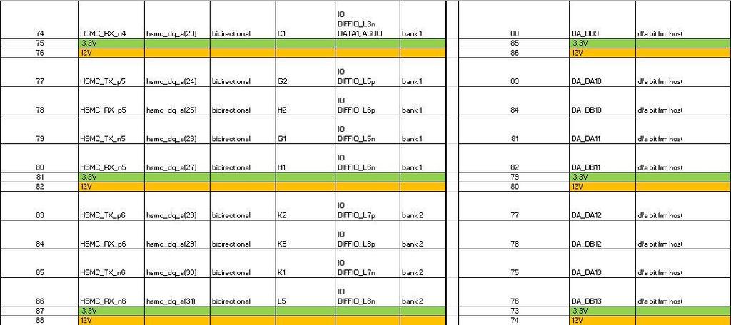
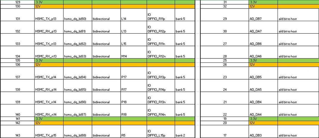
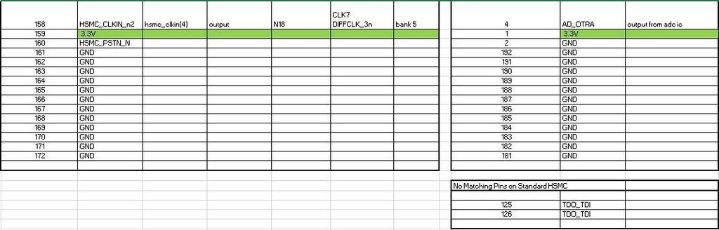
44 44 Cyclone III FPGA Starter Kit & THDB_ADA Daughter Board Pin Mapping

45 45


46 46

47 47

48 48
LFSRs as Functional Blocks in Wireless Applications Author: Stephen Lim and Andy Miller
 XAPP22 (v.) January, 2 R Application Note: Virtex Series, Virtex-II Series and Spartan-II family LFSRs as Functional Blocks in Wireless Applications Author: Stephen Lim and Andy Miller Summary Linear Feedback
THDB_ADA. High-Speed A/D and D/A Development Kit
 THDB_ADA High-Speed A/D and D/A Development Kit With complete reference design and source code for Fast-Fourier Transform analysis and arbitrary waveform generator. 1 CONTENTS Chapter 1 About the Kit...2
CSCB58 - Lab 4. Prelab /3 Part I (in-lab) /1 Part II (in-lab) /1 Part III (in-lab) /2 TOTAL /8
 /1 Part II (in-lab) /1 Part III (in-lab) /2 TOTAL /8") CSCB58 - Lab 4 Clocks and Counters Learning Objectives The purpose of this lab is to learn how to create counters and to be able to control when operations occur when the actual clock rate is much faster.
CSCB58 - Lab 4 Clocks and Counters Learning Objectives The purpose of this lab is to learn how to create counters and to be able to control when operations occur when the actual clock rate is much faster.
HDL & High Level Synthesize (EEET 2035) Laboratory II Sequential Circuits with VHDL: DFF, Counter, TFF and Timer
 Laboratory II Sequential Circuits with VHDL: DFF, Counter, TFF and Timer") 1 P a g e HDL & High Level Synthesize (EEET 2035) Laboratory II Sequential Circuits with VHDL: DFF, Counter, TFF and Timer Objectives: Develop the behavioural style VHDL code for D-Flip Flop using gated,
1 P a g e HDL & High Level Synthesize (EEET 2035) Laboratory II Sequential Circuits with VHDL: DFF, Counter, TFF and Timer Objectives: Develop the behavioural style VHDL code for D-Flip Flop using gated,
Laboratory 4. Figure 1: Serdes Transceiver
 Laboratory 4 The purpose of this laboratory exercise is to design a digital Serdes In the first part of the lab, you will design all the required subblocks for the digital Serdes and simulate them In part
FPGA Laboratory Assignment 4. Due Date: 06/11/2012
 FPGA Laboratory Assignment 4 Due Date: 06/11/2012 Aim The purpose of this lab is to help you understanding the fundamentals of designing and testing memory-based processing systems. In this lab, you will
FPGA Development for Radar, Radio-Astronomy and Communications
 John-Philip Taylor Room 7.03, Department of Electrical Engineering, Menzies Building, University of Cape Town Cape Town, South Africa 7701 Tel: +27 82 354 6741 email: tyljoh010@myuct.ac.za Internet: http://www.uct.ac.za
FPGA TechNote: Asynchronous signals and Metastability
 FPGA TechNote: Asynchronous signals and Metastability This Doulos FPGA TechNote gives a brief overview of metastability as it applies to the design of FPGAs. The first section introduces metastability
Chapter 5 Flip-Flops and Related Devices
 Chapter 5 Flip-Flops and Related Devices Chapter 5 Objectives Selected areas covered in this chapter: Constructing/analyzing operation of latch flip-flops made from NAND or NOR gates. Differences of synchronous/asynchronous
Laboratory 1 - Introduction to Digital Electronics and Lab Equipment (Logic Analyzers, Digital Oscilloscope, and FPGA-based Labkit)
") Massachusetts Institute of Technology Department of Electrical Engineering and Computer Science 6. - Introductory Digital Systems Laboratory (Spring 006) Laboratory - Introduction to Digital Electronics
Massachusetts Institute of Technology Department of Electrical Engineering and Computer Science 6. - Introductory Digital Systems Laboratory (Spring 006) Laboratory - Introduction to Digital Electronics
Experiment: FPGA Design with Verilog (Part 4)
") Department of Electrical & Electronic Engineering 2 nd Year Laboratory Experiment: FPGA Design with Verilog (Part 4) 1.0 Putting everything together PART 4 Real-time Audio Signal Processing In this part
Department of Electrical & Electronic Engineering 2 nd Year Laboratory Experiment: FPGA Design with Verilog (Part 4) 1.0 Putting everything together PART 4 Real-time Audio Signal Processing In this part
Implementing Audio IP in SDI II on Arria V Development Board
 Implementing Audio IP in SDI II on Arria V Development Board AN-697 Subscribe This document describes a reference design that uses the Audio Embed, Audio Extract, Clocked Audio Input and Clocked Audio
Scan. This is a sample of the first 15 pages of the Scan chapter.
 Scan This is a sample of the first 15 pages of the Scan chapter. Note: The book is NOT Pinted in color. Objectives: This section provides: An overview of Scan An introduction to Test Sequences and Test
[Krishna*, 4.(12): December, 2015] ISSN: (I2OR), Publication Impact Factor: 3.785
![[Krishna*, 4.(12): December, 2015] ISSN: (I2OR), Publication Impact Factor: 3.785](/thumbs/84/89645202.jpg "[Krishna*, 4.(12): December, 2015] ISSN: (I2OR), Publication Impact Factor: 3.785") IJESRT INTERNATIONAL JOURNAL OF ENGINEERING SCIENCES & RESEARCH TECHNOLOGY DESIGN AND IMPLEMENTATION OF BIST TECHNIQUE IN UART SERIAL COMMUNICATION M.Hari Krishna*, P.Pavan Kumar * Electronics and Communication
IJESRT INTERNATIONAL JOURNAL OF ENGINEERING SCIENCES & RESEARCH TECHNOLOGY DESIGN AND IMPLEMENTATION OF BIST TECHNIQUE IN UART SERIAL COMMUNICATION M.Hari Krishna*, P.Pavan Kumar * Electronics and Communication
Using SignalTap II in the Quartus II Software
 White Paper Using SignalTap II in the Quartus II Software Introduction The SignalTap II embedded logic analyzer, available exclusively in the Altera Quartus II software version 2.1, helps reduce verification
Design of Fault Coverage Test Pattern Generator Using LFSR
 Design of Fault Coverage Test Pattern Generator Using LFSR B.Saritha M.Tech Student, Department of ECE, Dhruva Institue of Engineering & Technology. Abstract: A new fault coverage test pattern generator
Radar Signal Processing Final Report Spring Semester 2017
 Radar Signal Processing Final Report Spring Semester 2017 Full report report by Brian Larson Other team members, Grad Students: Mohit Kumar, Shashank Joshil Department of Electrical and Computer Engineering
Static Timing Analysis for Nanometer Designs
 J. Bhasker Rakesh Chadha Static Timing Analysis for Nanometer Designs A Practical Approach 4y Spri ringer Contents Preface xv CHAPTER 1: Introduction / 1.1 Nanometer Designs 1 1.2 What is Static Timing
VHDL Design and Implementation of FPGA Based Logic Analyzer: Work in Progress
 VHDL Design and Implementation of FPGA Based Logic Analyzer: Work in Progress Nor Zaidi Haron Ayer Keroh +606-5552086 zaidi@utem.edu.my Masrullizam Mat Ibrahim Ayer Keroh +606-5552081 masrullizam@utem.edu.my
OpenXLR8: How to Load Custom FPGA Blocks
 OpenXLR8: How to Load Custom FPGA Blocks Webinar Breakdown: Introduc*on to pseudorandom number generator (LFSR) code Review of Verilog wrapper interface to microcontroller Simula*on with Mentor Graphics
Using on-chip Test Pattern Compression for Full Scan SoC Designs
 Using on-chip Test Pattern Compression for Full Scan SoC Designs Helmut Lang Senior Staff Engineer Jens Pfeiffer CAD Engineer Jeff Maguire Principal Staff Engineer Motorola SPS, System-on-a-Chip Design
Switching Solutions for Multi-Channel High Speed Serial Port Testing
 Switching Solutions for Multi-Channel High Speed Serial Port Testing Application Note by Robert Waldeck VP Business Development, ASCOR Switching The instruments used in High Speed Serial Port testing are
8. Stratix GX Built-In Self Test (BIST)
") 8. Stratix GX Built-In Self Test (BIST) SGX52008-1.1 Introduction Each Stratix GX channel in the gigabit transceiver block contains embedded built-in self test (BIST) circuitry, which is available for
8. Stratix GX Built-In Self Test (BIST) SGX52008-1.1 Introduction Each Stratix GX channel in the gigabit transceiver block contains embedded built-in self test (BIST) circuitry, which is available for
Objectives. Combinational logics Sequential logics Finite state machine Arithmetic circuits Datapath
 Objectives Combinational logics Sequential logics Finite state machine Arithmetic circuits Datapath In the previous chapters we have studied how to develop a specification from a given application, and
SignalTap Plus System Analyzer
 SignalTap Plus System Analyzer June 2000, ver. 1 Data Sheet Features Simultaneous internal programmable logic device (PLD) and external (board-level) logic analysis 32-channel external logic analyzer 166
NH 67, Karur Trichy Highways, Puliyur C.F, Karur District UNIT-III SEQUENTIAL CIRCUITS
 NH 67, Karur Trichy Highways, Puliyur C.F, 639 114 Karur District DEPARTMENT OF ELETRONICS AND COMMUNICATION ENGINEERING COURSE NOTES SUBJECT: DIGITAL ELECTRONICS CLASS: II YEAR ECE SUBJECT CODE: EC2203
BER MEASUREMENT IN THE NOISY CHANNEL
 BER MEASUREMENT IN THE NOISY CHANNEL PREPARATION... 2 overview... 2 the basic system... 3 a more detailed description... 4 theoretical predictions... 5 EXPERIMENT... 6 the ERROR COUNTING UTILITIES module...
Efficient Architecture for Flexible Prescaler Using Multimodulo Prescaler
 Efficient Architecture for Flexible Using Multimodulo G SWETHA, S YUVARAJ Abstract This paper, An Efficient Architecture for Flexible Using Multimodulo is an architecture which is designed from the proposed
Lab #10 Hexadecimal-to-Seven-Segment Decoder, 4-bit Adder-Subtractor and Shift Register. Fall 2017
 University of Texas at El Paso Electrical and Computer Engineering Department EE 2169 Laboratory for Digital Systems Design I Lab #10 Hexadecimal-to-Seven-Segment Decoder, 4-bit Adder-Subtractor and Shift
DE2-115/FGPA README. 1. Running the DE2-115 for basic operation. 2. The code/project files. Project Files
 DE2-115/FGPA README For questions email: jeff.nicholls.63@gmail.com (do not hesitate!) This document serves the purpose of providing additional information to anyone interested in operating the DE2-115
Troubleshooting EMI in Embedded Designs White Paper
 Troubleshooting EMI in Embedded Designs White Paper Abstract Today, engineers need reliable information fast, and to ensure compliance with regulations for electromagnetic compatibility in the most economical
INTERNATIONAL JOURNAL OF PURE AND APPLIED RESEARCH IN ENGINEERING AND TECHNOLOGY
 Tarannum Pathan,, 2013; Volume 1(8):655-662 INTERNATIONAL JOURNAL OF PURE AND APPLIED RESEARCH IN ENGINEERING AND TECHNOLOGY A PATH FOR HORIZING YOUR INNOVATIVE WORK VLSI IMPLEMENTATION OF 8, 16 AND 32
Altera JESD204B IP Core and ADI AD9144 Hardware Checkout Report
 2015.12.18 Altera JESD204B IP Core and ADI AD9144 Hardware Checkout Report AN-749 Subscribe The Altera JESD204B IP core is a high-speed point-to-point serial interface intellectual property (IP). The JESD204B
IT T35 Digital system desigm y - ii /s - iii
 UNIT - III Sequential Logic I Sequential circuits: latches flip flops analysis of clocked sequential circuits state reduction and assignments Registers and Counters: Registers shift registers ripple counters
TSIU03: Lab 3 - VGA. Petter Källström, Mario Garrido. September 10, 2018
 Petter Källström, Mario Garrido September 10, 2018 Abstract In the initialization of the DE2-115 (after you restart it), an image is copied into the SRAM memory. What you have to do in this lab is to read
AD9884A Evaluation Kit Documentation
 a (centimeters) AD9884A Evaluation Kit Documentation Includes Documentation for: - AD9884A Evaluation Board - SXGA Panel Driver Board Rev 0 1/4/2000 Evaluation Board Documentation For the AD9884A Purpose
hochschule fu r angewandte wissenschaften hamburg Prof. Dr. B. Schwarz FB Elektrotechnik/Informatik
 8 Shift Registers A Johnson counter contains the basic structure of a shift register which is made up by a chain of D- FFs. Beginning with the LSB of a register (a number of D-FFs) each D-FF output can
Digital Audio Design Validation and Debugging Using PGY-I2C
 Digital Audio Design Validation and Debugging Using PGY-I2C Debug the toughest I 2 S challenges, from Protocol Layer to PHY Layer to Audio Content Introduction Today s digital systems from the Digital
Debugging of Verilog Hardware Designs on Altera s DE-Series Boards. 1 Introduction. For Quartus Prime 15.1
 Debugging of Verilog Hardware Designs on Altera s DE-Series Boards For Quartus Prime 15.1 1 Introduction This tutorial presents some basic debugging concepts that can be helpful in creating Verilog designs
EXOSTIV TM. Frédéric Leens, CEO
 EXOSTIV TM Frédéric Leens, CEO A simple case: a video processing platform Headers & controls per frame : 1.024 bits 2.048 pixels 1.024 lines Pixels per frame: 2 21 Pixel encoding : 36 bit Frame rate: 24
VLSI Design: 3) Explain the various MOSFET Capacitances & their significance. 4) Draw a CMOS Inverter. Explain its transfer characteristics
 Explain the various MOSFET Capacitances & their significance. 4) Draw a CMOS Inverter. Explain its transfer characteristics") 1) Explain why & how a MOSFET works VLSI Design: 2) Draw Vds-Ids curve for a MOSFET. Now, show how this curve changes (a) with increasing Vgs (b) with increasing transistor width (c) considering Channel
1) Explain why & how a MOSFET works VLSI Design: 2) Draw Vds-Ids curve for a MOSFET. Now, show how this curve changes (a) with increasing Vgs (b) with increasing transistor width (c) considering Channel
Sharif University of Technology. SoC: Introduction
 SoC Design Lecture 1: Introduction Shaahin Hessabi Department of Computer Engineering System-on-Chip System: a set of related parts that act as a whole to achieve a given goal. A system is a set of interacting
A MISSILE INSTRUMENTATION ENCODER
 A MISSILE INSTRUMENTATION ENCODER Item Type text; Proceedings Authors CONN, RAYMOND; BREEDLOVE, PHILLIP Publisher International Foundation for Telemetering Journal International Telemetering Conference
Individual Project Report
 EN 3542: Digital Systems Design Individual Project Report Pseudo Random Number Generator using Linear Feedback shift registers Index No: Name: 110445D I.W.A.S.U. Premaratne 1. Problem: Random numbers are
Lab 3: VGA Bouncing Ball I
 CpE 487 Digital Design Lab Lab 3: VGA Bouncing Ball I 1. Introduction In this lab, we will program the FPGA on the Nexys2 board to display a bouncing ball on a 640 x 480 VGA monitor connected to the VGA
Metastability Analysis of Synchronizer
 Forn International Journal of Scientific Research in Computer Science and Engineering Research Paper Vol-1, Issue-3 ISSN: 2320 7639 Metastability Analysis of Synchronizer Ankush S. Patharkar *1 and V.
Laboratory Exercise 7
 Laboratory Exercise 7 Finite State Machines This is an exercise in using finite state machines. Part I We wish to implement a finite state machine (FSM) that recognizes two specific sequences of applied
Laboratory Exercise 4
 Laboratory Exercise 4 Polling and Interrupts The purpose of this exercise is to learn how to send and receive data to/from I/O devices. There are two methods used to indicate whether or not data can be
Decade Counters Mod-5 counter: Decade Counter:
 Decade Counters We can design a decade counter using cascade of mod-5 and mod-2 counters. Mod-2 counter is just a single flip-flop with the two stable states as 0 and 1. Mod-5 counter: A typical mod-5
UNIT IV CMOS TESTING. EC2354_Unit IV 1
 UNIT IV CMOS TESTING EC2354_Unit IV 1 Outline Testing Logic Verification Silicon Debug Manufacturing Test Fault Models Observability and Controllability Design for Test Scan BIST Boundary Scan EC2354_Unit
Achieving Timing Closure in ALTERA FPGAs
 Achieving Timing Closure in ALTERA FPGAs Course Description This course provides all necessary theoretical and practical know-how to write system timing constraints for variety designs in ALTERA FPGAs.
ECE 5765 Modern Communication Fall 2005, UMD Experiment 10: PRBS Messages, Eye Patterns & Noise Simulation using PRBS
 ECE 5765 Modern Communication Fall 2005, UMD Experiment 10: PRBS Messages, Eye Patterns & Noise Simulation using PRBS modules basic: SEQUENCE GENERATOR, TUNEABLE LPF, ADDER, BUFFER AMPLIFIER extra basic:
Serial FIR Filter. A Brief Study in DSP. ECE448 Spring 2011 Tuesday Section 15 points 3/8/2011 GEORGE MASON UNIVERSITY.
 GEORGE MASON UNIVERSITY Serial FIR Filter A Brief Study in DSP ECE448 Spring 2011 Tuesday Section 15 points 3/8/2011 Instructions: Zip all your deliverables into an archive .zip and submit it
SV1C Personalized SerDes Tester
 SV1C Personalized SerDes Tester Data Sheet SV1C Personalized SerDes Tester Data Sheet Revision: 1.0 2013-02-27 Revision Revision History Date 1.0 Document release Feb 27, 2013 The information in this
Debugging of VHDL Hardware Designs on Altera s DE2 Boards
 Debugging of VHDL Hardware Designs on Altera s DE2 Boards This tutorial presents some basic debugging concepts that can be helpful in creating VHDL designs for implementation on Altera s DE2 boards. It
Programmable Logic Design I
 Programmable Logic Design I Introduction In labs 11 and 12 you built simple logic circuits on breadboards using TTL logic circuits on 7400 series chips. This process is simple and easy for small circuits.
Smart Night Light. Figure 1: The state diagram for the FSM of the ALS.
 Smart Night Light Matt Ball, Aidan Faraji-Tajrishi, Thomas Goold, James Wallace Electrical and Computer Engineering Department School of Engineering and Computer Science Oakland University, Rochester,
EEM Digital Systems II
 ANADOLU UNIVERSITY DEPARTMENT OF ELECTRICAL AND ELECTRONICS ENGINEERING EEM 334 - Digital Systems II LAB 3 FPGA HARDWARE IMPLEMENTATION Purpose In the first experiment, four bit adder design was prepared
Experiment # 4 Counters and Logic Analyzer
 EE20L - Introduction to Digital Circuits Experiment # 4. Synopsis: Experiment # 4 Counters and Logic Analyzer In this lab we will build an up-counter and a down-counter using 74LS76A - Flip Flops. The
Design and FPGA Implementation of 100Gbit/s Scrambler Architectures for OTN Protocol Chethan Kumar M 1, Praveen Kumar Y G 2, Dr. M. Z. Kurian 3.
 International Journal of Computer Engineering and Applications, Volume VI, Issue II, May 14 www.ijcea.com ISSN 2321 3469 Design and FPGA Implementation of 100Gbit/s Scrambler Architectures for OTN Protocol
OFC & VLSI SIMULATION LAB MANUAL
 DEVBHOOMI INSTITUTE OF TECHNOLOGY FOR WOMEN, DEHRADUN - 24847 DEPARTMENT OF ELECTRONICS AND COMMUNICATION ENGINEERING Prepared BY: Ajay Kumar Gautam Asst. Prof. Electronics & Communication Engineering
UVM Testbench Structure and Coverage Improvement in a Mixed Signal Verification Environment by Mihajlo Katona, Head of Functional Verification, Frobas
 UVM Testbench Structure and Coverage Improvement in a Mixed Signal Verification Environment by Mihajlo Katona, Head of Functional Verification, Frobas In recent years a number of different verification
Synthesized Clock Generator
 Synthesized Clock Generator CG635 DC to 2.05 GHz low-jitter clock generator Clocks from DC to 2.05 GHz Random jitter
DT9834 Series High-Performance Multifunction USB Data Acquisition Modules
 DT9834 Series High-Performance Multifunction USB Data Acquisition Modules DT9834 Series High Performance, Multifunction USB DAQ Key Features: Simultaneous subsystem operation on up to 32 analog input channels,
Digital Transmission System Signaling Protocol EVLA Memorandum No. 33 Version 3
 Digital Transmission System Signaling Protocol EVLA Memorandum No. 33 Version 3 A modified version of Digital Transmission System Signaling Protocol, Written by Robert W. Freund, September 25, 2000. Prepared
Exercise 1-2. Digital Trunk Interface EXERCISE OBJECTIVE
 Exercise 1-2 Digital Trunk Interface EXERCISE OBJECTIVE When you have completed this exercise, you will be able to explain the role of the digital trunk interface in a central office. You will be familiar
Introduction to Fibre Optics
 Introduction to Fibre Optics White paper White Paper Introduction to Fibre Optics v1.0 EN 1 Introduction In today s networks, it is almost impossible to find a network professional who has never been in
Modeling Digital Systems with Verilog
 Modeling Digital Systems with Verilog Prof. Chien-Nan Liu TEL: 03-4227151 ext:34534 Email: jimmy@ee.ncu.edu.tw 6-1 Composition of Digital Systems Most digital systems can be partitioned into two types
Testing Results for a Video Poker System on a Chip
 Testing Results for a Video Poker System on a Chip Preston Thomson and Travis Johnson Introduction- This report examines the results of a system on a chip SoC video poker system. The report will begin
CHAPTER 3 EXPERIMENTAL SETUP
 CHAPTER 3 EXPERIMENTAL SETUP In this project, the experimental setup comprised of both hardware and software. Hardware components comprised of Altera Education Kit, capacitor and speaker. While software
Logic Analysis Basics
 Logic Analysis Basics September 27, 2006 presented by: Alex Dickson Copyright 2003 Agilent Technologies, Inc. Introduction If you have ever asked yourself these questions: What is a logic analyzer? What
Logic Analysis Basics
 Logic Analysis Basics September 27, 2006 presented by: Alex Dickson Copyright 2003 Agilent Technologies, Inc. Introduction If you have ever asked yourself these questions: What is a logic analyzer? What
Dual Slope ADC Design from Power, Speed and Area Perspectives
 Dual Slope ADC Design from Power, Speed and Area Perspectives Isaac Macwan, Xingguo Xiong, Lawrence Hmurcik Department of Electrical & Computer Engineering, University of Bridgeport, Bridgeport, CT 06604
Chapter 4: One-Shots, Counters, and Clocks
 Chapter 4: One-Shots, Counters, and Clocks I. The Monostable Multivibrator (One-Shot) The timing pulse is one of the most common elements of laboratory electronics. Pulses can control logical sequences
SignalTap Analysis in the Quartus II Software Version 2.0
 SignalTap Analysis in the Quartus II Software Version 2.0 September 2002, ver. 2.1 Application Note 175 Introduction As design complexity for programmable logic devices (PLDs) increases, traditional methods
FLIP-FLOPS AND RELATED DEVICES
 C H A P T E R 5 FLIP-FLOPS AND RELATED DEVICES OUTLINE 5- NAND Gate Latch 5-2 NOR Gate Latch 5-3 Troubleshooting Case Study 5-4 Digital Pulses 5-5 Clock Signals and Clocked Flip-Flops 5-6 Clocked S-R Flip-Flop
SignalTap: An In-System Logic Analyzer
 SignalTap: An In-System Logic Analyzer I. Introduction In this chapter we will learn 1 how to use SignalTap II (SignalTap) (Altera Corporation 2010). This core is a logic analyzer provided by Altera that
Experiment 7: Bit Error Rate (BER) Measurement in the Noisy Channel
 Measurement in the Noisy Channel") Experiment 7: Bit Error Rate (BER) Measurement in the Noisy Channel Modified Dr Peter Vial March 2011 from Emona TIMS experiment ACHIEVEMENTS: ability to set up a digital communications system over a noisy,
Experiment 7: Bit Error Rate (BER) Measurement in the Noisy Channel Modified Dr Peter Vial March 2011 from Emona TIMS experiment ACHIEVEMENTS: ability to set up a digital communications system over a noisy,
Design and Implementation of SOC VGA Controller Using Spartan-3E FPGA
 Design and Implementation of SOC VGA Controller Using Spartan-3E FPGA 1 ARJUNA RAO UDATHA, 2 B.SUDHAKARA RAO, 3 SUDHAKAR.B. 1 Dept of ECE, PG Scholar, 2 Dept of ECE, Associate Professor, 3 Electronics,
VLSI Technology used in Auto-Scan Delay Testing Design For Bench Mark Circuits
 VLSI Technology used in Auto-Scan Delay Testing Design For Bench Mark Circuits N.Brindha, A.Kaleel Rahuman ABSTRACT: Auto scan, a design for testability (DFT) technique for synchronous sequential circuits.
Optimization of Multi-Channel BCH Error Decoding for Common Cases. Russell Dill Master's Thesis Defense April 20, 2015
 Optimization of Multi-Channel BCH Error Decoding for Common Cases Russell Dill Master's Thesis Defense April 20, 2015 Bose-Chaudhuri-Hocquenghem (BCH) BCH is an Error Correcting Code (ECC) and is used
Prototyping an ASIC with FPGAs. By Rafey Mahmud, FAE at Synplicity.
 Prototyping an ASIC with FPGAs By Rafey Mahmud, FAE at Synplicity. With increased capacity of FPGAs and readily available off-the-shelf prototyping boards sporting multiple FPGAs, it has become feasible
GFT Channel Digital Delay Generator
 Features 20 independent delay Channels 100 ps resolution 25 ps rms jitter 10 second range Output pulse up to 6 V/50 Ω Independent trigger for every channel Fours Triggers Three are repetitive from three
AC : DIGITAL DESIGN MEETS DSP
 AC 2011-754: DIGITAL DESIGN MEETS DSP Christopher S Greene, University of Saint Thomas Christopher Greene received his Ph.D. in Electrical Engineering from the Massachusetts Institute of Technology (MIT)
Why FPGAs? FPGA Overview. Why FPGAs?
 Transistor-level Logic Circuits Positive Level-sensitive EECS150 - Digital Design Lecture 3 - Field Programmable Gate Arrays (FPGAs) January 28, 2003 John Wawrzynek Transistor Level clk clk clk Positive
Synchronous Sequential Logic
 Synchronous Sequential Logic Ranga Rodrigo August 2, 2009 1 Behavioral Modeling Behavioral modeling represents digital circuits at a functional and algorithmic level. It is used mostly to describe sequential
Reading an Image using CMOS Linear Image Sensor. S.R.Shinthu 1, P.Maheswari 2, C.S.Manikandababu 3. 1 Introduction. A.
 International Journal of Inventions in Computer Science and Engineering, Volume 2 Issue 4 April 2015 Reading an Image using CMOS Linear Image Sensor S.R.Shinthu 1, P.Maheswari 2, C.S.Manikandababu 3 1,2
FPGA IMPLEMENTATION AN ALGORITHM TO ESTIMATE THE PROXIMITY OF A MOVING TARGET
 International Journal of VLSI Design, 2(2), 20, pp. 39-46 FPGA IMPLEMENTATION AN ALGORITHM TO ESTIMATE THE PROXIMITY OF A MOVING TARGET Ramya Prasanthi Kota, Nagaraja Kumar Pateti2, & Sneha Ghanate3,2
Agilent E4430B 1 GHz, E4431B 2 GHz, E4432B 3 GHz, E4433B 4 GHz Measuring Bit Error Rate Using the ESG-D Series RF Signal Generators, Option UN7
 Agilent E4430B 1 GHz, E4431B 2 GHz, E4432B 3 GHz, E4433B 4 GHz Measuring Bit Error Rate Using the ESG-D Series RF Signal Generators, Option UN7 Product Note Introduction Bit-error-rate analysis As digital
Laboratory Exercise 7
 Laboratory Exercise 7 Finite State Machines This is an exercise in using finite state machines. Part I We wish to implement a finite state machine (FSM) that recognizes two specific sequences of applied
Lab #5: Design Example: Keypad Scanner and Encoder - Part 1 (120 pts)
") Nate Pihlstrom, npihlstr@uccs.edu Lab #5: Design Example: Keypad Scanner and Encoder - Part 1 (120 pts) Objective The objective of lab assignments 5 through 9 are to systematically design and implement
Nate Pihlstrom, npihlstr@uccs.edu Lab #5: Design Example: Keypad Scanner and Encoder - Part 1 (120 pts) Objective The objective of lab assignments 5 through 9 are to systematically design and implement
Logic Analyzer Triggering Techniques to Capture Elusive Problems
 Logic Analyzer Triggering Techniques to Capture Elusive Problems Efficient Solutions to Elusive Problems For digital designers who need to verify and debug their product designs, logic analyzers provide
Lab #12: 4-Bit Arithmetic Logic Unit (ALU)
") Lab #12: 4-Bit Arithmetic Logic Unit (ALU) ECE/COE 0501 Date of Experiment: 4/3/2017 Report Written: 4/5/2017 Submission Date: 4/10/2017 Nicholas Haver nicholas.haver@pitt.edu 1 H a v e r PURPOSE The purpose
Lab #12: 4-Bit Arithmetic Logic Unit (ALU) ECE/COE 0501 Date of Experiment: 4/3/2017 Report Written: 4/5/2017 Submission Date: 4/10/2017 Nicholas Haver nicholas.haver@pitt.edu 1 H a v e r PURPOSE The purpose
WINTER 15 EXAMINATION Model Answer
 Important Instructions to examiners: 1) The answers should be examined by key words and not as word-to-word as given in the model answer scheme. 2) The model answer and the answer written by candidate
EEC 116 Fall 2011 Lab #5: Pipelined 32b Adder
 EEC 116 Fall 2011 Lab #5: Pipelined 32b Adder Dept. of Electrical and Computer Engineering University of California, Davis Issued: November 2, 2011 Due: November 16, 2011, 4PM Reading: Rabaey Sections
2.6 Reset Design Strategy
 2.6 Reset esign Strategy Many design issues must be considered before choosing a reset strategy for an ASIC design, such as whether to use synchronous or asynchronous resets, will every flipflop receive
FPGA Implementation of Convolutional Encoder And Hard Decision Viterbi Decoder
 FPGA Implementation of Convolutional Encoder And Hard Decision Viterbi Decoder JTulasi, TVenkata Lakshmi & MKamaraju Department of Electronics and Communication Engineering, Gudlavalleru Engineering College,
CSE 352 Laboratory Assignment 3
 CSE 352 Laboratory Assignment 3 Introduction to Registers The objective of this lab is to introduce you to edge-trigged D-type flip-flops as well as linear feedback shift registers. Chapter 3 of the Harris&Harris
Application Note #63 Field Analyzers in EMC Radiated Immunity Testing
 Application Note #63 Field Analyzers in EMC Radiated Immunity Testing By Jason Galluppi, Supervisor Systems Control Software In radiated immunity testing, it is common practice to utilize a radio frequency
International Journal of Scientific & Engineering Research, Volume 5, Issue 9, September ISSN
 International Journal of Scientific & Engineering Research, Volume 5, Issue 9, September-2014 917 The Power Optimization of Linear Feedback Shift Register Using Fault Coverage Circuits K.YARRAYYA1, K CHITAMBARA