SoC Design Flow from DFT Engineers angle
|
|
|
- Jeremy Miller
- 6 years ago
- Views:
Transcription

1 SoC Design Flow from DFT Engineers angle Kang, Yong-Seok DIS Gr. / System IC Business Team
2 Agenda General SoC Design Flow and Guide DFT & Design Flow DFT Flow Conclusion
3 SoC Design Flow N MRD Architecture Spec. Marketing Requirements Doc. Product features Arch. at a higher level Optional Pseudo code/esl Verification IP, Transactors, scoreboards, checkers, Formal, Simulator Features that will be verified, testcases descriptions Arch. Validation Done? Y Y Verification Plan N Verification Environments A C Design Spec. RTL Design RTL Rule Clean? Y B FSM, FIFO, Clock, Reset, Interface descriptions Verilog/VHDL Syntax, Semantic, synthesis, P&R, DFT, LEC, Simulation, CDC
4 SoC design flow (Cont.) Really code frozen C A Design Verification Coverage Metrics N Verification Done? Y Tape out STA SDC B Synthesis Floorplan & Layout Parasitic + routed netlist Timing Analysis Synthesis SDC N DRC/DFM Timing OK? Y Area + Power Pin reports Package Selection Ball map
5 What is RTL? Register Transfer Level (RTL) description is a way of describing the operation of a synchronous digital circuit Synchronous circuit Register : Synchronize the circuit s operation Combinational logic : Performs all the logical functions RTL coding Declares the registers Describes the combination logic by using constructs such as ifthen-else and arithmetic operations Focuses on describing the flow of signals between registers All outputs of module/entity should be registered!
6 Clock Clocking One of the great innovations which enabled the semiconductor industry to progress to where it is today Quantizes time, enabling Trs to be abstracted to sequential state machines and from state machines into a simple and intuitive programming paradigm for chip design, RTL Fundamental assumption : Sequential execution All parts of a state machine stay in-step with respect to each other Flip-flop always makes a forward step from state n to state n+1 Setup conctraints No flip-flop ever makes more than one forward step from state n to state n+2 on a single clock tick Hold constraints
7 Clock Design First rule : Simple is Beautiful


8 Clock Design (Cont.) Second rule : Simple is Beautiful

 Third")

9 Clock Design (Cont.) Third rule : Simple is Beautiful
10 Clock Design ( Cont. ) Do not make masked clocks Do not use phase aligned clocks Do not use negative edge of source clock to make generatedclocks Do not use negative active clocks Do not use deep ripple-dividers in case of high speed designs All clocks should be generated in the separated clock generation module on the top hierarchy level In case of multiple clock sources, clock domain crossing should be checked Do not use manually gated clocks
11 Clock domain crossing issues Meta-stability Data from one clock domain may violate setup/hold time in the other clock domain Data loss Data from one clock domain may not hold long enough to be captured by the other clock domain Data correlation A group of conversing synchronized control signals are not in sync at a particular clock cycle Design intent More complex synchronization scheme (FIFO, handshake, C- element and etc.) may not behave as your spec.
12 Metastability General scientific concept which describes states of delicate equilibrium A system is in a metastable state when it is in equilibrium(not changing with time) but is susceptible to fall into lower-energy states with only slightly interaction Metastability in electronic circuits Metastability cannot be avoided, but the occurrences can be predicted by using the mean time between failures(mtbf) formula Designers can increase the MTBF using various synchronization schemes
13 Clock Gating Do not use manually gated clocks => Use enable signal Enable gclk Enable gclk Clock Clock posedge clk or negedge rst_n) begin If (!rst_n) q<=1 b0; else if ( enable ) q <=d; end CG cell for clock gating Glitch free No DFT problem RTL designers can consider free running clock Integrated clock gating cell w/o DFT Scan Enable Test Mode EN CLK Latch TSMC CG Cell GCLK
14 Reset Synchronous reset Asynchronous reset
15 Synchronous Reset Design Around 80+% of the gathered articles focused on synchronous reset issues in collection of ESNUG and SOLVE-IT articles Advantages Smaller flip-flops, but the combinational logic gate count grows, so the overall gate count savings may not be that significant The clock works as a filter for small reset glitches, however, if these glitches occur near the active clock edge, the flop could go metastable In some designs, the reset must be generated by a set of internal conditions. A synchronous reset is recommended for these types of designs because it will filter the logic equation glitches between clocks Disadvantage Need a pulse stretcher to guarantee a reset pulse width wide enough to ensure reset is present during an active edge of the clock During simulation, depending on how the reset is generated or how the reset is applied to a functional block, the reset can be masked by X s Timing closure problem exists if the reset is generated by combinational logic in the ASIC or if the reset must traverse many levels of local combinational logic If a gated clock is used to save power, the clock may be disabled coincident with the assertion of reset
16 Asynchronous Reset Design Advantages Data path is guaranteed to be clean Circuit can be reset with or without a clock present Synthesis interface tends to be automatic Disadvantage For DFT, asynchronous reset should be controllable The reset tree must be timed for both synchronous and asynchronous resets to ensure that the release of the reset can occur within one clock period Asynchronous reset can have, depending on its source, spurious resets due to noise or glitches on the board or system reset Attention must be paid to the release of the reset so as to prevent the chip from going into a metastable unknown state when reset is released.
17 Reset Design Guide Guideline I Every ASIC using an asynchronous reset should include a reset synchronizer circuit!!! Guideline II In general, change the testbench reset signal on the inactive clock edge using blocking assignments.
18 Reset Design Guide ( Cont. ) Reset-glitch filtering Multi-clock reset issues

19 Function verification Verification methodology

20 RTL Rule Check Sign-Off Flow

21 Logic Synthesis Do you remember Boolean algebra, Karnaugh maps, Quine-McCluskey algorithm, Espresso heuristic, and BDD? Logic synthesis Optimizes the Boolean equations generated by RTL synthesizers Maps them to technology specific gate-level implementations utilizing detailed functional and timing information from technology libraries. Operations in the logic synthesis process Multilevel minimization, factorization, and equation flattening Area, power, and timing metrics are optimized in some manner Resource sharing, arithmetic function architecting, topological approaches, congestion consideration
22 RTL Synthesizer Synopsys DC flow Timing is everything!!! The weight on timing constraints of the synthesis cost function is most critical
23 Design Constraints SDC (Synopsys Design Constraints) A common language between design processes Specify the design intent, including the timing, power, and area constraints for a design SDC Commands Operating conditions Wire load models System interface Design rule constraints Timing constraints Timing exceptions Area constraints Multi-voltage and power optimization constraints Logic assignments See Using the Synopsys Design Constraints Format, Application Note
24 Gate Level Simulation There are 3 kinds of homo sapiens on the earth Gate level simulation is not required Gate level simulation is required only in a zero-delay and ideal clock mode Fully back annotated simulation is a mandatory design flow Usefulness of gate level simulation Since scan and other test structures are added during and after synthesis, they are not checked by the RTL simulations and therefore need to be verified by gate level simulation Static timing analysis tools do not check asynchronous interfaces, so gate level simulation is required to look at the timing of these interfaces Careless wildcards in the static timing constraints set false path or multicycle path constraints where they don t belong Design changes, typos, or misunderstanding of the design can lead to incorrect false paths or multicycle paths in the static timing constraints Using create_clock instead of create_generated_clock leads to incorrect static timing between clock domains Gate level simulation can be used to collect switching factor data for power estimation X s in RTL simulation can be optimistic or pessimistic. The best way to verify that the design does not have any unintended dependence on initial conditions is to run gate level simulation It s a nice warm fuzzy that the design has been implemented correctly
25 Gate Level Simulation ( Cont. ) Sources of trouble in gate level simulation Issues caused by Library Models Pointing to Library Models Specify Blocks #1 Delays Pessimistic X propagation Issues caused by Design Registers that don t get reset Clock dividers Issues caused by Synthesis Synchronous reset back further into the middle of the logic cloud Incomplete Logic Optimization Interferes With Reset Feedback problems
26 Gate Level Simulation ( Cont. ) Sources of trouble in gate level simulation ( Cont. ) Issues when running SDF based gate level simulation Effects of timing failures : error messages can being caused by a false timing violation Expected Timing Violations Synchronizers for clock domain crossings Multi-cycle paths Guideline While some of the problems can be avoided through proper influence on your library vendor s models or proper design guidelines and planning, other problems will simply need to be addressed as they are encountered By knowing the areas where these problems can occur, we hope that you are able to more quickly find appropriate solutions
27 Auto Placement & Route Floorplanning Not practical now Jupiter ICC Virtual prototyping
28 Auto Placement & Route (Cont.) Tedious manual efforts reduction Timing correlation at each step (parasitics/xtalk/power/ocv) Zroute : QoR, Speed, DFM

29 Importance of CTS Ideal clock model vs. propagated clock model An ideal clock model of timing simplifies the propagated clocks model of timing by assuming that the launch and capture clock paths have the same delay Clock based design is itself often referred to as synchronous design even though there is nothing fundamentally synchronous about clock based design itself! Role of CTS Chip design begins in a ideal clock world but ends in a propagated clock worlds Transition between these two worlds Balanced Clocks Design Flow
30 Clocks Tree under 65nm
31 Low power design Power dissipation
 Power management")
32 Low power design ( Cont. ) Power management spectrum
33 Low Power Methodology Comparison Low power Design methods Multi-Vt Long channel Source/ Back bias Fine grain footer Coarse grain header Coarse grain footer Dynamic Volt/Freq Scaling (DVFS) AVS TSMC low power library & IP Multi-Vt library Long cha nnel library Tapless li brary, ta p cell Cell with foot er, retention FF Header/footer switch, mother-daughter switch, switch for always_on rows, retention FF, isolation cell IEM, Single heigh t level shifter AVS IP, Level Shifter Power Reduction Active leakage Active leakage Active leakage Standby leakage Standby leakage Standby Leakage Dynamic & active Leakage Dynamic & active leakage Dyn pwr Reduction (30%VDD) 50% (7%VDD) 10~15% Leakage Reduction 2~10x base 7%~15% 2x~10x 10x 30x ~ 60x 60x ~ 120x 3x 10~20% Area Overhead 0% ~0% 2% 5%~15% 4%~6% 2%~3%+DNW 2%~5% 2% Performance Penalty no no no 2%~4% 2%~4% 2%~4% no no Data Retentio n yes yes yes yes (HVT), retention FF Retention FF Extra PG Retention FF Extra PG yes VCCmin Retention Extra PG Voltage Regulator needed no no yes no no no yes yes
34 Agenda General SoC Design Flow and Guide DFT & Design Flow DFT Flow Conclusion
35 DFT Strategy : Design specification step Digital core Scan MBIST Fault models Hierarchical approaches Compression Multi-mode Power/Test time Test clock RTL vs netlist level insertion # of controller Power TAP or TAPless Test clock IO Digital IO boundary scan Analog IO High speed IO SERDES Tx/Rx Ad-hoc Isolation test BIST Multi-site test Parallel test ATE Test options Memory capacity Available signaling speed Vector format Board design System level test Go/no-go test HW/SW preparation
36 DFT Rule Check : RTL design step Clock rules Do not switch on both edges of a clock Do not use data as clocks No "ANDing" of generated clocks No logic in common with clock and data Asynchronous rules Active phase of all set and reset pins buffer connected to the same root level pin must be the same level Do not use flip-flops with both asynchronous set & reset Set and reset lines on the same flip-flop should not be simultaneously active Latch rules Do not use latches unless transparent during power ground mode No combinational loops from transparent latches No synchronous latches Tri-state rules Do not infer tristatecomponents Tristatebuses should have a pull-up or pull-down connection Tristatebus enables must be fully decoded so that exactly one driver is active at any time
37 Scan clocking Stuck-at At-speed


38 Multiple scan clock Advantages - Compact test patterns - Short ATPG run time Disadvantages -Careful clock analysis - CTS for test mode - No flexibility Advantages -Safest approach - Flexibility Disadvantages - More sharing pins - Large patterns - Huge ATPG run time to reduce pattern size

39 Clock Domain Crossing Scan shift mode Lock-up latch/skew clock Capture mode Clock domain Analysis : False path, Multi-cycle path, CDC Capture by clock/capture by clock group/fine CTS for test clocks shift hold capture reshift shift 1. RTZ 2. RTZ 3. RTZ 4. RTZ 5. RTZ 6. RTZ 7. DN RZ DEFAULT_TS DEFAULT_TS HOLD_TS HOLD_TS LAUNCH_TS CAPTURE_TS LAUNCH_TS CAPTURE_TS LAUNCH_TS CAPTURE_TS LAUNCH_TS CAPTURE_TS LAUNCH_TS CAPTURE_TS LAUNCH_TS CAPTURE_TS DEFAULT_TS DEFAULT_TS DEFAULT_TS 1ns
40 Design constraints : Synthesis/P&R/STA At least 3 design constraints are required Scan shift/scan capture MBIST Iterate, one mode/corner at a time, hoping next run doesn t break previous Clock definition mode1.sdc mode2.sdc mode3.sdc Test clock and function clock False path, multi-cycle path On chip clocking Synthesis /P&R Synthesis /P&R Synthesis /P&R Test modes Hold timing violation Huge area overhead Manually merge constraints and manage overlaps, conflicts, etc mode1.sdc mode3.sdc mode2.sdc? merge.sdc MCMM is mandatory
41 Agenda General SoC Design Flow and Guide DFT & Design Flow DFT Flow Conclusion

42 DFT Flow in Real Fields Source from TSMC

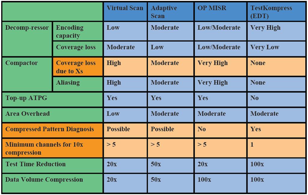
43 Scan Compression Source from MentorGraphics


44 Physically Aware ATPG Slack-aware tests : Small delay defects ATPG selects observation path with lowest slack Source from Magma Layout-aware tests Bridge defects, single via defects, crosstalk defects
45 Low Power Test Problem : Scan Typical ATPG will target as many faults as possible May cause a large number of flip-flops (FF) toggling May exceed the design power intent or limits May cause unintended ATE failures, or worse, product damage Problem : MBIST Typical MBIST will target as many memories as possible Solution Clock gating (ATPG and DFT) Low toggling (ATPG or DFT) Trade-off between test time and power consumption (MBIST ) Dynamic power analysis for test modes

46
TKK S ASIC-PIIRIEN SUUNNITTELU
 Design TKK S-88.134 ASIC-PIIRIEN SUUNNITTELU Design Flow 3.2.2005 RTL Design 10.2.2005 Implementation 7.4.2005 Contents 1. Terminology 2. RTL to Parts flow 3. Logic synthesis 4. Static Timing Analysis
2.6 Reset Design Strategy
 2.6 Reset esign Strategy Many design issues must be considered before choosing a reset strategy for an ASIC design, such as whether to use synchronous or asynchronous resets, will every flipflop receive
Design for Testability
 TDTS 01 Lecture 9 Design for Testability Zebo Peng Embedded Systems Laboratory IDA, Linköping University Lecture 9 The test problems Fault modeling Design for testability techniques Zebo Peng, IDA, LiTH
Static Timing Analysis for Nanometer Designs
 J. Bhasker Rakesh Chadha Static Timing Analysis for Nanometer Designs A Practical Approach 4y Spri ringer Contents Preface xv CHAPTER 1: Introduction / 1.1 Nanometer Designs 1 1.2 What is Static Timing
Scan. This is a sample of the first 15 pages of the Scan chapter.
 Scan This is a sample of the first 15 pages of the Scan chapter. Note: The book is NOT Pinted in color. Objectives: This section provides: An overview of Scan An introduction to Test Sequences and Test
EITF35: Introduction to Structured VLSI Design
 EITF35: Introduction to Structured VLSI Design Part 4.2.1: Learn More Liang Liu liang.liu@eit.lth.se 1 Outline Crossing clock domain Reset, synchronous or asynchronous? 2 Why two DFFs? 3 Crossing clock
Using on-chip Test Pattern Compression for Full Scan SoC Designs
 Using on-chip Test Pattern Compression for Full Scan SoC Designs Helmut Lang Senior Staff Engineer Jens Pfeiffer CAD Engineer Jeff Maguire Principal Staff Engineer Motorola SPS, System-on-a-Chip Design
Lecture 23 Design for Testability (DFT): Full-Scan
: Full-Scan") Lecture 23 Design for Testability (DFT): Full-Scan (Lecture 19alt in the Alternative Sequence) Definition Ad-hoc methods Scan design Design rules Scan register Scan flip-flops Scan test sequences Overheads
Lecture 23 Design for Testability (DFT): Full-Scan (Lecture 19alt in the Alternative Sequence) Definition Ad-hoc methods Scan design Design rules Scan register Scan flip-flops Scan test sequences Overheads
System IC Design: Timing Issues and DFT. Hung-Chih Chiang
 System IC esign: Timing Issues and FT Hung-Chih Chiang Outline SoC Timing Issues Timing terminologies Synchronous vs. asynchronous design Interfaces and timing closure Clocking issues Reset esign for Testability
K.T. Tim Cheng 07_dft, v Testability
 K.T. Tim Cheng 07_dft, v1.0 1 Testability Is concept that deals with costs associated with testing. Increase testability of a circuit Some test cost is being reduced Test application time Test generation
Clock Domain Crossing. Presented by Abramov B. 1
 Clock Domain Crossing Presented by Abramov B. 1 Register Transfer Logic Logic R E G I S T E R Transfer Logic R E G I S T E R Presented by Abramov B. 2 RTL (cont) An RTL circuit is a digital circuit composed
 Page 1 of 6 Follow these guidelines to design testable ASICs, boards, and systems. (includes related article on automatic testpattern generation basics) (Tutorial) From: EDN Date: August 19, 1993 Author:
for Digital IC's Design-for-Test and Embedded Core Systems Alfred L. Crouch Prentice Hall PTR Upper Saddle River, NJ
 Design-for-Test for Digital IC's and Embedded Core Systems Alfred L. Crouch Prentice Hall PTR Upper Saddle River, NJ 07458 www.phptr.com ISBN D-13-DflMfla7-l : Ml H Contents Preface Acknowledgments Introduction
Chapter 2 Clocks and Resets
 Chapter 2 Clocks and Resets 2.1 Introduction The cost of designing ASICs is increasing every year. In addition to the non-recurring engineering (NRE) and mask costs, development costs are increasing due
At-speed Testing of SOC ICs
 At-speed Testing of SOC ICs Vlado Vorisek, Thomas Koch, Hermann Fischer Multimedia Design Center, Semiconductor Products Sector Motorola Munich, Germany Abstract This paper discusses the aspects and associated
Achieving Timing Closure in ALTERA FPGAs
 Achieving Timing Closure in ALTERA FPGAs Course Description This course provides all necessary theoretical and practical know-how to write system timing constraints for variety designs in ALTERA FPGAs.
DEDICATED TO EMBEDDED SOLUTIONS
 DEDICATED TO EMBEDDED SOLUTIONS DESIGN SAFE FPGA INTERNAL CLOCK DOMAIN CROSSINGS ESPEN TALLAKSEN DATA RESPONS SCOPE Clock domain crossings (CDC) is probably the worst source for serious FPGA-bugs that
Lecture 23 Design for Testability (DFT): Full-Scan (chapter14)
: Full-Scan (chapter14)") Lecture 23 Design for Testability (DFT): Full-Scan (chapter14) Definition Ad-hoc methods Scan design Design rules Scan register Scan flip-flops Scan test sequences Overheads Scan design system Summary
Lecture 23 Design for Testability (DFT): Full-Scan (chapter14) Definition Ad-hoc methods Scan design Design rules Scan register Scan flip-flops Scan test sequences Overheads Scan design system Summary
Figure 1 shows a simple implementation of a clock switch, using an AND-OR type multiplexer logic.
 1. CLOCK MUXING: With more and more multi-frequency clocks being used in today's chips, especially in the communications field, it is often necessary to switch the source of a clock line while the chip
Testability: Lecture 23 Design for Testability (DFT) Slide 1 of 43
 Slide 1 of 43") Testability: Lecture 23 Design for Testability (DFT) Shaahin hi Hessabi Department of Computer Engineering Sharif University of Technology Adapted, with modifications, from lecture notes prepared p by
Testability: Lecture 23 Design for Testability (DFT) Shaahin hi Hessabi Department of Computer Engineering Sharif University of Technology Adapted, with modifications, from lecture notes prepared p by
EE178 Spring 2018 Lecture Module 5. Eric Crabill
 EE178 Spring 2018 Lecture Module 5 Eric Crabill Goals Considerations for synchronizing signals Clocks Resets Considerations for asynchronous inputs Methods for crossing clock domains Clocks The academic
Chapter 8 Design for Testability
 電機系 Chapter 8 Design for Testability 測試導向設計技術 2 Outline Introduction Ad-Hoc Approaches Full Scan Partial Scan 3 Design For Testability Definition Design For Testability (DFT) refers to those design techniques
Overview: Logic BIST
 VLSI Design Verification and Testing Built-In Self-Test (BIST) - 2 Mohammad Tehranipoor Electrical and Computer Engineering University of Connecticut 23 April 2007 1 Overview: Logic BIST Motivation Built-in
Asynchronous IC Interconnect Network Design and Implementation Using a Standard ASIC Flow
 Asynchronous IC Interconnect Network Design and Implementation Using a Standard ASIC Flow Bradley R. Quinton*, Mark R. Greenstreet, Steven J.E. Wilton*, *Dept. of Electrical and Computer Engineering, Dept.
Design of Fault Coverage Test Pattern Generator Using LFSR
 Design of Fault Coverage Test Pattern Generator Using LFSR B.Saritha M.Tech Student, Department of ECE, Dhruva Institue of Engineering & Technology. Abstract: A new fault coverage test pattern generator
At-speed testing made easy
 At-speed testing made easy By Bruce Swanson and Michelle Lange, EEdesign.com Jun 03, 2004 (5:00 PM EDT) URL: http://www.eedesign.com/article/showarticle.jhtml?articleid=21401421 Today's chip designs are
Testing Digital Systems II
 Testing Digital Systems II Lecture 2: Design for Testability (I) structor: M. Tahoori Copyright 2010, M. Tahoori TDS II: Lecture 2 1 History During early years, design and test were separate The final
Synchronization in Asynchronously Communicating Digital Systems
 Synchronization in Asynchronously Communicating Digital Systems Priyadharshini Shanmugasundaram Abstract Two digital systems working in different clock domains require a protocol to communicate with each
DEPARTMENT OF ELECTRICAL &ELECTRONICS ENGINEERING DIGITAL DESIGN
 DEPARTMENT OF ELECTRICAL &ELECTRONICS ENGINEERING DIGITAL DESIGN Assoc. Prof. Dr. Burak Kelleci Spring 2018 OUTLINE Synchronous Logic Circuits Latch Flip-Flop Timing Counters Shift Register Synchronous
1. What does the signal for a static-zero hazard look like?
 Sample Problems 1. What does the signal for a static-zero hazard look like? The signal will always be logic zero except when the hazard occurs which will cause it to temporarly go to logic one (i.e. glitch
Sharif University of Technology. SoC: Introduction
 SoC Design Lecture 1: Introduction Shaahin Hessabi Department of Computer Engineering System-on-Chip System: a set of related parts that act as a whole to achieve a given goal. A system is a set of interacting
Objectives. Combinational logics Sequential logics Finite state machine Arithmetic circuits Datapath
 Objectives Combinational logics Sequential logics Finite state machine Arithmetic circuits Datapath In the previous chapters we have studied how to develop a specification from a given application, and
EE178 Lecture Module 4. Eric Crabill SJSU / Xilinx Fall 2005
 EE178 Lecture Module 4 Eric Crabill SJSU / Xilinx Fall 2005 Lecture #9 Agenda Considerations for synchronizing signals. Clocks. Resets. Considerations for asynchronous inputs. Methods for crossing clock
Asynchronous & Synchronous Reset Design Techniques - Part Deux
 Clifford E. Cummings Don Mills Steve Golson Sunburst Design, Inc. LCDM Engineering Trilobyte Systems cliffc@sunburst-design.com mills@lcdm-eng.com sgolson@trilobyte.com ABSTRACT This paper will investigate
Timing Error Detection: An Adaptive Scheme To Combat Variability EE241 Final Report Nathan Narevsky and Richard Ott {nnarevsky,
 Timing Error Detection: An Adaptive Scheme To Combat Variability EE241 Final Report Nathan Narevsky and Richard Ott {nnarevsky, tomott}@berkeley.edu Abstract With the reduction of feature sizes, more sources
Low Power Illinois Scan Architecture for Simultaneous Power and Test Data Volume Reduction
 Low Illinois Scan Architecture for Simultaneous and Test Data Volume Anshuman Chandra, Felix Ng and Rohit Kapur Synopsys, Inc., 7 E. Middlefield Rd., Mountain View, CA Abstract We present Low Illinois
UNIT IV CMOS TESTING. EC2354_Unit IV 1
 UNIT IV CMOS TESTING EC2354_Unit IV 1 Outline Testing Logic Verification Silicon Debug Manufacturing Test Fault Models Observability and Controllability Design for Test Scan BIST Boundary Scan EC2354_Unit
4 of 40. Multi-ASIC reset synchronization Good Multi-Flip-Flop. Synthesis issues with reset nets. 3 of 40. Synchronous Resets? Asynchronous Resets?
 Synchronous Resets? Asynchronous Resets? I am so confused! How will I ever know which to use? &OLIIRUG(&XPPLQJV 'RQLOOV 6XQEXUVW'HVLJQ,Q /&'(QJLQHHULQJ OLII#VXQEXUVWGHVLJQRP PLOOV#OGPHQJRP ZZZVXQEXUVWGHVLJQRP
Combinational vs Sequential
 Combinational vs Sequential inputs X Combinational Circuits outputs Z A combinational circuit: At any time, outputs depends only on inputs Changing inputs changes outputs No regard for previous inputs
Prototyping an ASIC with FPGAs. By Rafey Mahmud, FAE at Synplicity.
 Prototyping an ASIC with FPGAs By Rafey Mahmud, FAE at Synplicity. With increased capacity of FPGAs and readily available off-the-shelf prototyping boards sporting multiple FPGAs, it has become feasible
Jin-Fu Li Advanced Reliable Systems (ARES) Laboratory. National Central University
 Laboratory. National Central University") Chapter 3 Basics of VLSI Testing (2) Jin-Fu Li Advanced Reliable Systems (ARES) Laboratory Department of Electrical Engineering National Central University Jhongli, Taiwan Outline Testing Process Fault
Chapter 3 Basics of VLSI Testing (2) Jin-Fu Li Advanced Reliable Systems (ARES) Laboratory Department of Electrical Engineering National Central University Jhongli, Taiwan Outline Testing Process Fault
Laboratory 1 - Introduction to Digital Electronics and Lab Equipment (Logic Analyzers, Digital Oscilloscope, and FPGA-based Labkit)
") Massachusetts Institute of Technology Department of Electrical Engineering and Computer Science 6. - Introductory Digital Systems Laboratory (Spring 006) Laboratory - Introduction to Digital Electronics
Massachusetts Institute of Technology Department of Electrical Engineering and Computer Science 6. - Introductory Digital Systems Laboratory (Spring 006) Laboratory - Introduction to Digital Electronics
VirtualScan TM An Application Story
 Test Data Compaction Tool from SynTest TM VirtualScan TM An Application Story January 29, 2004 Hiroshi Furukawa SoC No. 3 Group, SoC Development Division 1 Agenda Current Problems What is VirtualScan?
CS/EE 6710 Digital VLSI Design CAD Assignment #3 Due Thursday September 21 st, 5:00pm
 CS/EE 6710 Digital VLSI Design CAD Assignment #3 Due Thursday September 21 st, 5:00pm Overview: In this assignment you will design a register cell. This cell should be a single-bit edge-triggered D-type
4. Formal Equivalence Checking
 4. Formal Equivalence Checking 1 4. Formal Equivalence Checking Jacob Abraham Department of Electrical and Computer Engineering The University of Texas at Austin Verification of Digital Systems Spring
Low Power VLSI Circuits and Systems Prof. Ajit Pal Department of Computer Science and Engineering Indian Institute of Technology, Kharagpur
 Low Power VLSI Circuits and Systems Prof. Ajit Pal Department of Computer Science and Engineering Indian Institute of Technology, Kharagpur Lecture No. # 29 Minimizing Switched Capacitance-III. (Refer
System IC Design: Timing Issues and DFT. Hung-Chih Chiang
 Wireless Information Transmission System Lab. System IC esign: Timing Issues and FT Hung-Chih Chiang Institute of Communications Engineering National Sun Yat-sen University SoC Timing Issues Outline Timing
DC Ultra. Concurrent Timing, Area, Power and Test Optimization. Overview
 DATASHEET DC Ultra Concurrent Timing, Area, Power and Test Optimization DC Ultra RTL synthesis solution enables users to meet today s design challenges with concurrent optimization of timing, area, power
Powerful Software Tools and Methods to Accelerate Test Program Development A Test Systems Strategies, Inc. (TSSI) White Paper.
 White Paper.") Powerful Software Tools and Methods to Accelerate Test Program Development A Test Systems Strategies, Inc. (TSSI) White Paper Abstract Test costs have now risen to as much as 50 percent of the total manufacturing
Powerful Software Tools and Methods to Accelerate Test Program Development A Test Systems Strategies, Inc. (TSSI) White Paper Abstract Test costs have now risen to as much as 50 percent of the total manufacturing
https://daffy1108.wordpress.com/2014/06/08/synchronizers-for-asynchronous-signals/
 https://daffy1108.wordpress.com/2014/06/08/synchronizers-for-asynchronous-signals/ Synchronizers for Asynchronous Signals Asynchronous signals causes the big issue with clock domains, namely metastability.
Lecture 17: Introduction to Design For Testability (DFT) & Manufacturing Test
 & Manufacturing Test") Lecture 17: Introduction to Design For Testability (DFT) & Manufacturing Test Mark McDermott Electrical and Computer Engineering The University of Texas at Austin Agenda Introduction to testing Logical
Lecture 17: Introduction to Design For Testability (DFT) & Manufacturing Test Mark McDermott Electrical and Computer Engineering The University of Texas at Austin Agenda Introduction to testing Logical
Report on 4-bit Counter design Report- 1, 2. Report on D- Flipflop. Course project for ECE533
 Report on 4-bit Counter design Report- 1, 2. Report on D- Flipflop Course project for ECE533 I. Objective: REPORT-I The objective of this project is to design a 4-bit counter and implement it into a chip
Sequential Circuits. Output depends only and immediately on the inputs Have no memory (dependence on past values of the inputs)
") Sequential Circuits Combinational circuits Output depends only and immediately on the inputs Have no memory (dependence on past values of the inputs) Sequential circuits Combination circuits with memory
Sequential Circuits Combinational circuits Output depends only and immediately on the inputs Have no memory (dependence on past values of the inputs) Sequential circuits Combination circuits with memory
Clock - key to synchronous systems. Topic 7. Clocking Strategies in VLSI Systems. Latch vs Flip-Flop. Clock for timing synchronization
 Clock - key to synchronous systems Topic 7 Clocking Strategies in VLSI Systems Peter Cheung Department of Electrical & Electronic Engineering Imperial College London Clocks help the design of FSM where
Clock - key to synchronous systems. Lecture 7. Clocking Strategies in VLSI Systems. Latch vs Flip-Flop. Clock for timing synchronization
 Clock - key to synchronous systems Lecture 7 Clocking Strategies in VLSI Systems Peter Cheung Department of Electrical & Electronic Engineering Imperial College London Clocks help the design of FSM where
Based on slides/material by. Topic 14. Testing. Testing. Logic Verification. Recommended Reading:
 Based on slides/material by Topic 4 Testing Peter Y. K. Cheung Department of Electrical & Electronic Engineering Imperial College London!! K. Masselos http://cas.ee.ic.ac.uk/~kostas!! J. Rabaey http://bwrc.eecs.berkeley.edu/classes/icbook/instructors.html
FSM Cookbook. 1. Introduction. 2. What Functional Information Must be Modeled
 FSM Cookbook 1. Introduction Tau models describe the timing and functional information of component interfaces. Timing information specifies the delay in placing values on output signals and the timing
Static Timing Analysis for Nanometer Designs. A Practical Approach
 Static Timing Analysis for Nanometer Designs A Practical Approach J. Bhasker Rakesh Chadha Static Timing Analysis for Nanometer Designs A Practical Approach J. Bhasker Rakesh Chadha esilicon Corporation
Random Access Scan. Veeraraghavan Ramamurthy Dept. of Electrical and Computer Engineering Auburn University, Auburn, AL
 Random Access Scan Veeraraghavan Ramamurthy Dept. of Electrical and Computer Engineering Auburn University, Auburn, AL ramamve@auburn.edu Term Paper for ELEC 7250 (Spring 2005) Abstract: Random Access
EECS150 - Digital Design Lecture 19 - Finite State Machines Revisited
 EECS150 - Digital Design Lecture 19 - Finite State Machines Revisited April 2, 2013 John Wawrzynek Spring 2013 EECS150 - Lec19-fsm Page 1 Finite State Machines (FSMs) FSM circuits are a type of sequential
11. Sequential Elements
 11. Sequential Elements Jacob Abraham Department of Electrical and Computer Engineering The University of Texas at Austin VLSI Design Fall 2017 October 11, 2017 ECE Department, University of Texas at Austin
A video signal processor for motioncompensated field-rate upconversion in consumer television
 A video signal processor for motioncompensated field-rate upconversion in consumer television B. De Loore, P. Lippens, P. Eeckhout, H. Huijgen, A. Löning, B. McSweeney, M. Verstraelen, B. Pham, G. de Haan,
Software Engineering 2DA4. Slides 9: Asynchronous Sequential Circuits
 Software Engineering 2DA4 Slides 9: Asynchronous Sequential Circuits Dr. Ryan Leduc Department of Computing and Software McMaster University Material based on S. Brown and Z. Vranesic, Fundamentals of
Level and edge-sensitive behaviour
 Level and edge-sensitive behaviour Asynchronous set/reset is level-sensitive Include set/reset in sensitivity list Put level-sensitive behaviour first: process (clock, reset) is begin if reset = '0' then
Simulation Mismatches Can Foul Up Test-Pattern Verification
 1 of 5 12/17/2009 2:59 PM Technologies Design Hotspots Resources Shows Magazine ebooks & Whitepapers Jobs More... Click to view this week's ad screen [ D e s i g n V i e w / D e s i g n S o lu ti o n ]
Sequential Circuit Design: Principle
 Sequential Circuit Design: Principle modified by L.Aamodt 1 Outline 1. 2. 3. 4. 5. 6. 7. 8. Overview on sequential circuits Synchronous circuits Danger of synthesizing asynchronous circuit Inference of
LFSRs as Functional Blocks in Wireless Applications Author: Stephen Lim and Andy Miller
 XAPP22 (v.) January, 2 R Application Note: Virtex Series, Virtex-II Series and Spartan-II family LFSRs as Functional Blocks in Wireless Applications Author: Stephen Lim and Andy Miller Summary Linear Feedback
IT T35 Digital system desigm y - ii /s - iii
 UNIT - III Sequential Logic I Sequential circuits: latches flip flops analysis of clocked sequential circuits state reduction and assignments Registers and Counters: Registers shift registers ripple counters
Designs with Multiple Clock Domains: Avoiding Clock Skew and Reducing Pattern Count Using DFTAdvisor tm and FastScan tm
 Technical Publication esigns with Multiple Clock omains: Avoiding Clock Skew and Reducing Pattern Count Using FTAdvisor tm and FastScan tm Mentor Graphics Corporation March 2001 www.mentor.com/dft esigns
EL302 DIGITAL INTEGRATED CIRCUITS LAB #3 CMOS EDGE TRIGGERED D FLIP-FLOP. Due İLKER KALYONCU, 10043
 EL302 DIGITAL INTEGRATED CIRCUITS LAB #3 CMOS EDGE TRIGGERED D FLIP-FLOP Due 16.05. İLKER KALYONCU, 10043 1. INTRODUCTION: In this project we are going to design a CMOS positive edge triggered master-slave
cascading flip-flops for proper operation clock skew Hardware description languages and sequential logic
 equential logic equential circuits simple circuits with feedback latches edge-triggered flip-flops Timing methodologies cascading flip-flops for proper operation clock skew Basic registers shift registers
NH 67, Karur Trichy Highways, Puliyur C.F, Karur District UNIT-III SEQUENTIAL CIRCUITS
 NH 67, Karur Trichy Highways, Puliyur C.F, 639 114 Karur District DEPARTMENT OF ELETRONICS AND COMMUNICATION ENGINEERING COURSE NOTES SUBJECT: DIGITAL ELECTRONICS CLASS: II YEAR ECE SUBJECT CODE: EC2203
FPGA TechNote: Asynchronous signals and Metastability
 FPGA TechNote: Asynchronous signals and Metastability This Doulos FPGA TechNote gives a brief overview of metastability as it applies to the design of FPGAs. The first section introduces metastability
Sequencing. Lan-Da Van ( 范倫達 ), Ph. D. Department of Computer Science National Chiao Tung University Taiwan, R.O.C. Fall,
, Ph. D. Department of Computer Science National Chiao Tung University Taiwan, R.O.C. Fall,") Sequencing ( 范倫達 ), Ph. D. Department of Computer Science National Chiao Tung University Taiwan, R.O.C. Fall, 2013 ldvan@cs.nctu.edu.tw http://www.cs.nctu.edu.tw/~ldvan/ Outlines Introduction Sequencing
Sequencing ( 范倫達 ), Ph. D. Department of Computer Science National Chiao Tung University Taiwan, R.O.C. Fall, 2013 ldvan@cs.nctu.edu.tw http://www.cs.nctu.edu.tw/~ldvan/ Outlines Introduction Sequencing
Project 6: Latches and flip-flops
 Project 6: Latches and flip-flops Yuan Ze University epartment of Computer Engineering and Science Copyright by Rung-Bin Lin, 1999 All rights reserved ate out: 06/5/2003 ate due: 06/25/2003 Purpose: This
Metastability Analysis of Synchronizer
 Forn International Journal of Scientific Research in Computer Science and Engineering Research Paper Vol-1, Issue-3 ISSN: 2320 7639 Metastability Analysis of Synchronizer Ankush S. Patharkar *1 and V.
Microprocessor Design
 Microprocessor Design Principles and Practices With VHDL Enoch O. Hwang Brooks / Cole 2004 To my wife and children Windy, Jonathan and Michelle Contents 1. Designing a Microprocessor... 2 1.1 Overview
Lec 24 Sequential Logic Revisited Sequential Circuit Design and Timing
 Traversing igital esign EECS - Components and esign Techniques for igital Systems EECS wks 6 - Lec 24 Sequential Logic Revisited Sequential Circuit esign and Timing avid Culler Electrical Engineering and
CHAPTER 4: Logic Circuits
 CHAPTER 4: Logic Circuits II. Sequential Circuits Combinational circuits o The outputs depend only on the current input values o It uses only logic gates, decoders, multiplexers, ALUs Sequential circuits
Figure.1 Clock signal II. SYSTEM ANALYSIS
 International Journal of Advances in Engineering, 2015, 1(4), 518-522 ISSN: 2394-9260 (printed version); ISSN: 2394-9279 (online version); url:http://www.ijae.in RESEARCH ARTICLE Multi bit Flip-Flop Grouping
Chapter 5: Synchronous Sequential Logic
 Chapter 5: Synchronous Sequential Logic NCNU_2016_DD_5_1 Digital systems may contain memory for storing information. Combinational circuits contains no memory elements the outputs depends only on the inputs
Sequential logic. Circuits with feedback. How to control feedback? Sequential circuits. Timing methodologies. Basic registers
 equential logic equential circuits simple circuits with feedback latches edge-triggered flip-flops Timing methodologies cascading flip-flops for proper operation clock skew Basic registers shift registers
Chapter 4. Logic Design
 Chapter 4 Logic Design 4.1 Introduction. In previous Chapter we studied gates and combinational circuits, which made by gates (AND, OR, NOT etc.). That can be represented by circuit diagram, truth table
MC9211 Computer Organization
 MC9211 Computer Organization Unit 2 : Combinational and Sequential Circuits Lesson2 : Sequential Circuits (KSB) (MCA) (2009-12/ODD) (2009-10/1 A&B) Coverage Lesson2 Outlines the formal procedures for the
BUSES IN COMPUTER ARCHITECTURE
 BUSES IN COMPUTER ARCHITECTURE The processor, main memory, and I/O devices can be interconnected by means of a common bus whose primary function is to provide a communication path for the transfer of data.
VARIABLE FREQUENCY CLOCKING HARDWARE
 VARIABLE FREQUENCY CLOCKING HARDWARE Variable-Frequency Clocking Hardware Many complex digital systems have components clocked at different frequencies Reason 1: to reduce power dissipation The active
EEC 116 Fall 2011 Lab #5: Pipelined 32b Adder
 EEC 116 Fall 2011 Lab #5: Pipelined 32b Adder Dept. of Electrical and Computer Engineering University of California, Davis Issued: November 2, 2011 Due: November 16, 2011, 4PM Reading: Rabaey Sections
Computer Architecture and Organization
 A-1 Appendix A - Digital Logic Computer Architecture and Organization Miles Murdocca and Vincent Heuring Appendix A Digital Logic A-2 Appendix A - Digital Logic Chapter Contents A.1 Introduction A.2 Combinational
Boolean, 1s and 0s stuff: synthesis, verification, representation This is what happens in the front end of the ASIC design process
 (Lec 11) From Logic To Layout What you know... Boolean, 1s and 0s stuff: synthesis, verification, representation This is what happens in the front end of the ASIC design process High-level design description
More on Flip-Flops Digital Design and Computer Architecture: ARM Edition 2015 Chapter 3 <98> 98
 More on Flip-Flops Digital Design and Computer Architecture: ARM Edition 2015 Chapter 3 98 Review: Bit Storage SR latch S (set) Q R (reset) Level-sensitive SR latch S S1 C R R1 Q D C S R D latch Q
Lab #5: Design Example: Keypad Scanner and Encoder - Part 1 (120 pts)
") Nate Pihlstrom, npihlstr@uccs.edu Lab #5: Design Example: Keypad Scanner and Encoder - Part 1 (120 pts) Objective The objective of lab assignments 5 through 9 are to systematically design and implement
Nate Pihlstrom, npihlstr@uccs.edu Lab #5: Design Example: Keypad Scanner and Encoder - Part 1 (120 pts) Objective The objective of lab assignments 5 through 9 are to systematically design and implement
Impact of Test Point Insertion on Silicon Area and Timing during Layout
 Impact of Test Point Insertion on Silicon Area and Timing during Layout Harald Vranken Ferry Syafei Sapei 2 Hans-Joachim Wunderlich 2 Philips Research Laboratories IC Design Digital Design & Test Prof.
Chapter 10 Exercise Solutions
 VLSI Test Principles and Architectures Ch. 10 oundary Scan & Core-ased Testing P. 1/10 Chapter 10 Exercise Solutions 10.1 The following is just an example for testing chips and interconnects on a board.
A Low Power Delay Buffer Using Gated Driver Tree
 IOSR Journal of VLSI and Signal Processing (IOSR-JVSP) ISSN: 2319 4200, ISBN No. : 2319 4197 Volume 1, Issue 4 (Nov. - Dec. 2012), PP 26-30 A Low Power Delay Buffer Using Gated Driver Tree Kokkilagadda
EEE2135 Digital Logic Design Chapter 6. Latches/Flip-Flops and Registers/Counters 서강대학교 전자공학과
 EEE235 Digital Logic Design Chapter 6. Latches/Flip-Flops and Registers/Counters 서강대학교 전자공학과 . Delay and Latches ) Signal Storage a. as voltage level static memory b. as charges dynamic memory 2) Delays
CHAPTER 4: Logic Circuits
 CHAPTER 4: Logic Circuits II. Sequential Circuits Combinational circuits o The outputs depend only on the current input values o It uses only logic gates, decoders, multiplexers, ALUs Sequential circuits
International Journal of Scientific & Engineering Research, Volume 5, Issue 9, September ISSN
 International Journal of Scientific & Engineering Research, Volume 5, Issue 9, September-2014 917 The Power Optimization of Linear Feedback Shift Register Using Fault Coverage Circuits K.YARRAYYA1, K CHITAMBARA
Logic Design for On-Chip Test Clock Generation- Implementation Details and Impact on Delay Test Quality
 Logic Design for On-Chip Test Clock Generation- mplementation Details and mpact on Delay Test Quality Beck, Olivier Barondeau, Martin Kaibel, Frank Poehl Technologies AG 73 81541Munich, Germany Xijiang
EEC 118 Lecture #9: Sequential Logic. Rajeevan Amirtharajah University of California, Davis Jeff Parkhurst Intel Corporation
 EEC 118 Lecture #9: Sequential Logic Rajeevan Amirtharajah University of California, Davis Jeff Parkhurst Intel Corporation Outline Review: Static CMOS Logic Finish Static CMOS transient analysis Sequential
VLSI Technology used in Auto-Scan Delay Testing Design For Bench Mark Circuits
 VLSI Technology used in Auto-Scan Delay Testing Design For Bench Mark Circuits N.Brindha, A.Kaleel Rahuman ABSTRACT: Auto scan, a design for testability (DFT) technique for synchronous sequential circuits.