Digital Circuits ECS 371
|
|
|
- Shon Park
- 5 years ago
- Views:
Transcription
1 Digital Circuits ECS 37 Dr. Prapun Suksompong Lecture 0 Office Hours: BKD Monday 9:00-0:30, :30-3:30 Tuesday 0:30-:30
2 Announcement HW4 posted on the course web site Chapter 5: 4(b,c,e), 20a, 22a, 56 Write down all the steps that you have done to obtain your answers. Due date: July 6, 2009 (Thursday) There will be a quiz today. 2
3 Review NAND gate is a universal gate. NOR gate is a universal gate. 3
4 NAND Gate as a Universal Gate NAND gates are sometimes called universal gates because they can be used to produce the other basic Boolean functions. A Inverter A A B AND gate AB A B A + B A B A + B OR gate NOR gate 4


5 Example Implement the following logic circuit using only NAND gates: Solution: C Negative-OR NAND C 5 C


6 Example Implement the following logic circuit using only NAND gates: Solution: Negative-OR NAND It is easy to turn AND-OR configuration into a NANDgate-only circuit 6
7 NOR Gate as a Universal Gate NOR gates are also universal gates and can form all of the basic gates. A Inverter A A B OR gate A + B A B AB A B AB AND gate NAND gate 7
8 Example Implement the following logic circuit using only NOR gates: Solution: 8
9 Combinational Logic We studied the theoretical principles used in combinational logic design. We will build on that foundation and describe many of the devices, structures, and methods used by engineers to solve practical digital design problems. A complex circuit or system is conceived as a collection of smaller subsystems, each of which has a much simpler description. 9
10 Digital System Concept A digital system is an arrangement of the individual logic functions connected to perform a specified operation or produce a defined output. 0

11 Combinational Building Blocks There are several straightforward structures that turn up quite regularly as building blocks in larger systems. Encoder Decoders Comparators Multiplexers Where can we find these building blocks?
12 Fixed-function IC An integrated circuit (IC) is an electronic circuit that is constructed entirely on a single small chip of silicon. Two broad categories of digital ICs.. Fixed-function logic 2. Programmable logic In fixed-function logic, the logic functions are set by the manufacturer and cannot be changed. 2
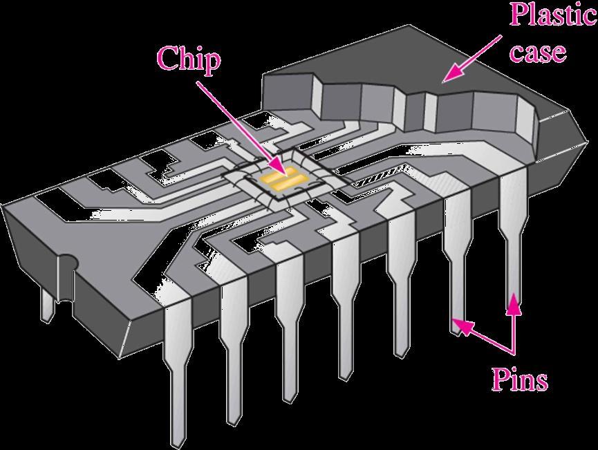
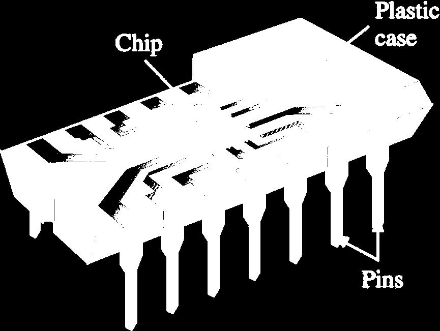

13 Fixed-function IC package 3 Cutaway view of DIP (Dual-In-line Pins) chip
14 Complexity Classifications Fixed-function digital lcs are classified according to their complexity. Small-scale integration (SSI) up to ten equivalent gate circuits on a single chip basic gates and flip-flops. Medium-scale integration (MSI) from 0 to 00 equivalent gates on a chip. encoders, decoders, counters, registers, multiplexers, arithmetic circuits, small memories Large-scale integration (LSI) Very large-scale integration (VLSI) Ultra large-scale integration (ULSI) 4

15 SSI 74x00 5

16 MSI For the next couple lectures, we will study most of these 74-series MSI. 6
17 MSI 7 DECODER C D B A GN G2N O0N O2N O5N O0N ON ON O3N O4N O4N O3N O2N O7N O6N O5N O9N O8N 7454 inst BCD TO DEC D B C A O7N O8N O9N O0N O3N O2N ON O6N O5N O4N 7442 inst BCD TO 7SEG LTN B C D RBIN BIN A OB OC OE OD OF OG OA RBON 7447 inst2 COMPARATOR A3 B2 A2 AEBI AGBI ALBI A0 B0 B3 A B ALBO AGBO AEBO 7485 inst3 3:8 DECODER A B G C G2AN G2BN Y0N YN Y2N Y3N Y4N Y5N Y6N Y7N 7438 inst4 2:4 DECODER A A2 B B2 GN G2N Y0N Y20N Y3N Y2N YN Y2N Y22N Y23N 7439 inst5 ENCODER N 2N 3N 6N 5N 4N 9N 8N 7N CN BN AN DN 7447 inst6 ENCODER 5N 0N N 2N 3N 4N EIN 6N 7N AN A0N A2N EON GSN 7448 inst7 MULTIPLEXER GN C B A D5 D0 D D4 D3 D2 D6 D7 Y WN 745 inst8 MULTIPLEXER A B SEL B2 A3 B3 A2 B4 GN A4 Y2 Y Y4 Y inst9 PARITY GEN. B A F E D I C G H EVEN ODD inst0 4 BIT ADDER CIN A A2 B2 A3 A4 B4 B B3 SUM4 COUT SUM SUM2 SUM inst
18 Simple Decoder A decoder is a logic circuit that detects the presence of a specific combination of bits at its input. Two simple decoders that detect the presence of the binary code 00 are shown below. The first has an active HIGH output; the second has an active LOW output. A 0 A X A 0 A X A 2 A 2 A 3 A 3 Active HIGH decoder for 00 Active LOW decoder for 00 8 (A 0 is the LSB and A 3 is the MSB)
19 Exercise Assume the output of the decoder shown below is a logic. What are the inputs to the decoder? A 0 = 0 A = A 2 = 0 A 3 = 9
20 Binary-to-Decimal Decoder The binary-to-decimal decoder shown here has 6 outputs one for each combination of binary inputs. 4-bit binary input 0 A 0 A A 2 A 3 Bin/Dec The bubbles indicate active- LOW outputs. Decimal outputs 20
 ports.")
21 Application: Port Address Decoder Decoder can be used in computers for input/output selection. Computers communicate with peripherals by sending and/or receiving data through what is known as input/output (I/O) ports. A decoder can be used to select the I/O port so that data can be sent or received from a specific external device. 2

22 2:4 decoder 2-to-4 line decoder with enable input 22
23 Exercise Find the truth table of the -to-2 line decoder below. Then, implement the -to-2 line decoder. I Y0 Y 23


24 74x39: Dual 2:4 Decoder Two independent 2:4 decoders The outputs and the enable (E) input are active-low. When E is HIGH all outputs are forced HIGH. Most MSI decoders were originally designed with active- LOW output. E O 3 24 Notice that all of the signal names inside the symbol outline are active-high, and that bubbles indicate active-low inputs and outputs.

25 25 74x39
26 74x39: Logic diagram Active- LOW Enable This is a usual 2:4 decoder. 26 Active-LOW output because NAND gates are used instead of AND gates
27 Example: Building a larger decoder Construct a 3-to-8 decoder from two 2-to-4 decoders Notice that this part is equivalent to a :2 decoder. How can we add an active-high enable input? 27 Low order bits (A, A 0 ) select within decoders. High order bit (A 2 ) controls which decoder is active.
28 Building larger decoder from smaller ones To construct (k+n)-to-2 n+k decoders, can use. 2 n of k-to-2 k decoders with enable input and 2. one n-to-2n decoders. The connections are: For each of the k-to-2 k decoder with enable input, all have k input we put in A 0 A k-. The enable line of the r th decoder is connected to D r of the n-to-2 n decoders. The inputs of the n-to-2 n decoder get A k to A n+k-. Basically, each k-to-2 k decoder works on the last k bits. We use the first n bit, via the n-to-2 n decoder, to select which one (and only one) of the k-to-2 k decoders will be enabled. 28
29 Example Construct a 4:6 decoder with an active-low enable from three 2:4 decoders. 29

30 74x38: 3:8 Decoder Active-LOW outputs Three enable inputs. 30
31 Example Construct a 4:6 decoder with an active-low enable (EN) from two 74x38 decoder. 3


32 Example Construct a 5:32 decoder with two activelow enable and one active-high enable from four 74x38 and one 74x39. 32
 HIGH.")

33 74x54: 4:6 Decoder A LOW level on each chip select input is required to make the enable gate output (EN) HIGH. Include two active-low chip select (CS) lines which must be at the active level to enable the outputs. These lines can be used to expand the decoder to larger inputs. Alternative logic symbol 33 inst DECODER A B C D GN G2N 7454 O0N ON O2N O3N O4N O5N O6N O7N O8N O9N O0N ON O2N O3N O4N O5N

34 34 5:32 Decoder

35 Decoder as general purpose logic Any combinational circuit with n inputs and m outputs can be implemented with an n-to-2 n -line decoder and m OR gate Observe that the 3:8 decoder generates all possible minterms. 35
 C =")

36 Example Implement a full adder circuit with a decoder and OR gates S = X,Y,Z (,2,4,7) C = X,Y,Z (3,5,6,7) 36 Inputs Outputs X Y Z C A B C in C out S S
 we will talk about other types of decoder.")
37 Other Decoders In general, a decoder converts coded information, such as binary number, into non-coded form. Later, (if time permitted) we will talk about other types of decoder. 37
EEE130 Digital Electronics I Lecture #1_2. Dr. Shahrel A. Suandi
 EEE130 Digital Electronics I Lecture #1_2 Dr. Shahrel A. Suandi 1-4 Overview of Basic Logic Functions Digital systems are generally built from combinations of NOT, AND and OR logic elements The combinations
DIGITAL CIRCUIT LOGIC UNIT 9: MULTIPLEXERS, DECODERS, AND PROGRAMMABLE LOGIC DEVICES
 DIGITAL CIRCUIT LOGIC UNIT 9: MULTIPLEXERS, DECODERS, AND PROGRAMMABLE LOGIC DEVICES 1 Learning Objectives 1. Explain the function of a multiplexer. Implement a multiplexer using gates. 2. Explain the
1. Convert the decimal number to binary, octal, and hexadecimal.
 1. Convert the decimal number 435.64 to binary, octal, and hexadecimal. 2. Part A. Convert the circuit below into NAND gates. Insert or remove inverters as necessary. Part B. What is the propagation delay
Experiment (6) 2- to 4 Decoder. Figure 8.1 Block Diagram of 2-to-4 Decoder 0 X X
 2- to 4 Decoder. Figure 8.1 Block Diagram of 2-to-4 Decoder 0 X X") 8. Objectives : Experiment (6) Decoders / Encoders To study the basic operation and design of both decoder and encoder circuits. To describe the concept of active low and active-high logic signals. To
8. Objectives : Experiment (6) Decoders / Encoders To study the basic operation and design of both decoder and encoder circuits. To describe the concept of active low and active-high logic signals. To
A Combined Combinational-Sequential System
 A Combined Combinational-Sequential System Object To construct a serial transmission circuit with a comparator to check the output. Parts () 7485 4-bit magnitude comparators (1) 74177 4-bit binary counter
gate symbols will appear in schematic Dierent of a circuit. Standard gate symbols have been diagram Figures 5-3 and 5-4 show standard shapes introduce
 chapter is concerned with examples of basic This circuits including decoders, combinational xor gate and parity circuits, multiplexers, comparators, adders. Those basic building circuits frequently and
TYPICAL QUESTIONS & ANSWERS
 DIGITALS ELECTRONICS TYPICAL QUESTIONS & ANSWERS OBJECTIVE TYPE QUESTIONS Each Question carries 2 marks. Choose correct or the best alternative in the following: Q.1 The NAND gate output will be low if
DIGITAL SYSTEM DESIGN UNIT I (2 MARKS)
") DIGITAL SYSTEM DESIGN UNIT I (2 MARKS) 1. Convert Binary number (111101100) 2 to Octal equivalent. 2. Convert Binary (1101100010011011) 2 to Hexadecimal equivalent. 3. Simplify the following Boolean function
DIGITAL SYSTEM DESIGN UNIT I (2 MARKS) 1. Convert Binary number (111101100) 2 to Octal equivalent. 2. Convert Binary (1101100010011011) 2 to Hexadecimal equivalent. 3. Simplify the following Boolean function
UNIVERSITY OF MASSACHUSSETS LOWELL Department of Electrical & Computer Engineering Course Syllabus for Logic Design Fall 2013
 UNIVERSITY OF MASSACHUSSETS LOWELL Department of Electrical & Computer Engineering Course Syllabus for 16.265 Logic Design Fall 2013 I. General Information Section 201 Instructor: Professor Anh Tran Office
EXPERIMENT: 1. Graphic Symbol: OR: The output of OR gate is true when one of the inputs A and B or both the inputs are true.
 EXPERIMENT: 1 DATE: VERIFICATION OF BASIC LOGIC GATES AIM: To verify the truth tables of Basic Logic Gates NOT, OR, AND, NAND, NOR, Ex-OR and Ex-NOR. APPARATUS: mention the required IC numbers, Connecting
(Refer Slide Time: 1:45)
") (Refer Slide Time: 1:45) Digital Circuits and Systems Prof. S. Srinivasan Department of Electrical Engineering Indian Institute of Technology, Madras Lecture - 30 Encoders and Decoders So in the last lecture
(Refer Slide Time: 1:45) Digital Circuits and Systems Prof. S. Srinivasan Department of Electrical Engineering Indian Institute of Technology, Madras Lecture - 30 Encoders and Decoders So in the last lecture
WELCOME. ECE 2030: Introduction to Computer Engineering* Richard M. Dansereau Copyright by R.M. Dansereau,
 CHAPTER I- CHAPTER I WELCOME TO ECE 23: Introduction to Computer Engineering* Richard M. Dansereau rdanse@pobox.com Copyright by R.M. Dansereau, 2-2 * ELEMENTS OF NOTES AFTER W. KINSNER, UNIVERSITY OF
PHYSICS 5620 LAB 9 Basic Digital Circuits and Flip-Flops
 PHYSICS 5620 LAB 9 Basic Digital Circuits and Flip-Flops Objective Construct a two-bit binary decoder. Study multiplexers (MUX) and demultiplexers (DEMUX). Construct an RS flip-flop from discrete gates.
Bachelor Level/ First Year/ Second Semester/ Science Full Marks: 60 Computer Science and Information Technology (CSc. 151) Pass Marks: 24
 Pass Marks: 24") 2065 Computer Science and Information Technology (CSc. 151) Pass Marks: 24 Time: 3 hours. Candidates are required to give their answers in their own words as for as practicable. Attempt any TWO questions:
2065 Computer Science and Information Technology (CSc. 151) Pass Marks: 24 Time: 3 hours. Candidates are required to give their answers in their own words as for as practicable. Attempt any TWO questions:
THE KENYA POLYTECHNIC
 THE KENYA POLYTECHNIC ELECTRICAL/ELECTRONICS ENGINEERING DEPARTMENT HIGHER DIPLOMA IN ELECTRICAL ENGINEERING END OF YEAR II EXAMINATIONS NOVEMBER 006 DIGITAL ELECTRONICS 3 HOURS INSTRUCTIONS TO CANDIDATES:
The word digital implies information in computers is represented by variables that take a limited number of discrete values.
 Class Overview Cover hardware operation of digital computers. First, consider the various digital components used in the organization and design. Second, go through the necessary steps to design a basic
Find the equivalent decimal value for the given value Other number system to decimal ( Sample)
") VELAMMAL COLLEGE OF ENGINEERING AND TECHNOLOGY, MADURAI 65 009 Department of Information Technology Model Exam-II-Question bank PART A (Answer for all Questions) (8 X = 6) K CO Marks Find the equivalent
VELAMMAL COLLEGE OF ENGINEERING AND TECHNOLOGY, MADURAI 65 009 Department of Information Technology Model Exam-II-Question bank PART A (Answer for all Questions) (8 X = 6) K CO Marks Find the equivalent
MODULE 3. Combinational & Sequential logic
 MODULE 3 Combinational & Sequential logic Combinational Logic Introduction Logic circuit may be classified into two categories. Combinational logic circuits 2. Sequential logic circuits A combinational
Laboratory Objectives and outcomes for Digital Design Lab
 Class: SE Department of Information Technology Subject Logic Design Sem : III Course Objectives and outcomes for LD Course Objectives: Students will try to : COB1 Understand concept of various components.
Theory Lecture Day Topic Practical Day. Week. number systems and their inter-conversion Decimal, Binary. 3rd. 1st. 1st
 Lesson Plan Name of the Faculty : Priyanka Nain Discipline: Electronics & Communication Engg. Semester:5th Subject:DEMP Lesson Plan Duration: 15 Weeks Work Load(Lecture/Practical) per week (In Hours):
ECE Lab 5. MSI Circuits - Four-Bit Adder/Subtractor with Decimal Output
 ECE 201 - Lab 5 MSI Circuits - Four-Bit Adder/Subtractor with Decimal Output PURPOSE To familiarize students with Medium Scale Integration (MSI) technology, specifically adders. The student should also
TIME SCHEDULE. MODULE TOPICS PERIODS 1 Number system & Boolean algebra 17 Test I 1 2 Logic families &Combinational logic
 COURSE TITLE : DIGITAL INSTRUMENTS PRINCIPLE COURSE CODE : 3075 COURSE CATEGORY : B PERIODS/WEEK : 4 PERIODS/SEMESTER : 72 CREDITS : 4 TIME SCHEDULE MODULE TOPICS PERIODS 1 Number system & Boolean algebra
Digital Networks and Systems Laboratory 2 Basic Digital Building Blocks Time 4 hours
 Digital Networks and Systems Laboratory 2 Basic Digital Building Blocks Time 4 hours Aim To investigate the basic digital circuit building blocks constructed from combinatorial logic or dedicated Integrated
Minnesota State College Southeast
 ELEC 2211: Digital Electronics II A. COURSE DESCRIPTION Credits: 4 Lecture Hours/Week: 2 Lab Hours/Week: 4 OJT Hours/Week: *.* Prerequisites: None Corequisites: None MnTC Goals: None Minnesota State College
Digital Circuits ECS 371
 igital Circuits ECS 371 r. Prapun Suksompong prapun@siit.tu.ac.th Lecture 17 Office Hours: BK 3601-7 Monday 9:00-10:30, 1:30-3:30 Tuesday 10:30-11:30 1 Announcement Reading Assignment: Chapter 7: 7-1,
R13 SET - 1 '' ''' '' ' '''' Code No: RT21053
 SET - 1 1. a) What are the characteristics of 2 s complement numbers? b) State the purpose of reducing the switching functions to minimal form. c) Define half adder. d) What are the basic operations in
Contents Circuits... 1
 Contents Circuits... 1 Categories of Circuits... 1 Description of the operations of circuits... 2 Classification of Combinational Logic... 2 1. Adder... 3 2. Decoder:... 3 Memory Address Decoder... 5 Encoder...
Chapter Contents. Appendix A: Digital Logic. Some Definitions
 A- Appendix A - Digital Logic A-2 Appendix A - Digital Logic Chapter Contents Principles of Computer Architecture Miles Murdocca and Vincent Heuring Appendix A: Digital Logic A. Introduction A.2 Combinational
Encoders and Decoders: Details and Design Issues
 Encoders and Decoders: Details and Design Issues Edward L. Bosworth, Ph.D. TSYS School of Computer Science Columbus State University Columbus, GA 31907 bosworth_edward@colstate.edu Slide 1 of 25 slides
NORTHWESTERN UNIVERSITY TECHNOLOGICAL INSTITUTE
 NORTHWESTERN UNIVERSITY TECHNOLOGICL INSTITUTE ECE 270 Experiment #8 DIGITL CIRCUITS Prelab 1. Draw the truth table for the S-R Flip-Flop as shown in the textbook. Draw the truth table for Figure 7. 2.
Lab #11: Register Files
 Lab #11: Register Files ECE/COE 0501 Date of Experiment: 3/20/2017 Report Written: 3/22/2017 Submission Date: 3/27/2017 Nicholas Haver nicholas.haver@pitt.edu 1 H a v e r PURPOSE The purpose of this lab
1. True/False Questions (10 x 1p each = 10p) (a) I forgot to write down my name and student ID number.
 (a) I forgot to write down my name and student ID number.") CprE 281: Digital Logic Midterm 2: Friday Oct 30, 2015 Student Name: Student ID Number: Lab Section: Mon 9-12(N) Mon 12-3(P) Mon 5-8(R) Tue 11-2(U) (circle one) Tue 2-5(M) Wed 8-11(J) Wed 6-9(Y) Thur 11-2(Q)
CprE 281: Digital Logic Midterm 2: Friday Oct 30, 2015 Student Name: Student ID Number: Lab Section: Mon 9-12(N) Mon 12-3(P) Mon 5-8(R) Tue 11-2(U) (circle one) Tue 2-5(M) Wed 8-11(J) Wed 6-9(Y) Thur 11-2(Q)
The reduction in the number of flip-flops in a sequential circuit is referred to as the state-reduction problem.
 State Reduction The reduction in the number of flip-flops in a sequential circuit is referred to as the state-reduction problem. State-reduction algorithms are concerned with procedures for reducing the
Chapter 8 Functions of Combinational Logic
 ETEC 23 Programmable Logic Devices Chapter 8 Functions of Combinational Logic Shawnee State University Department of Industrial and Engineering Technologies Copyright 27 by Janna B. Gallaher Basic Adders
WINTER 15 EXAMINATION Model Answer
 Important Instructions to examiners: 1) The answers should be examined by key words and not as word-to-word as given in the model answer scheme. 2) The model answer and the answer written by candidate
Half-Adders. Ch.5 Summary. Chapter 5. Thomas L. Floyd
 Digital Fundamentals: A Systems Approach Functions of Combinational Logic Chapter 5 Half-Adders Basic rules of binary addition are performed by a half adder, which accepts two binary inputs (A and B) and
DEPARTMENT OF COMPUTER SCIENCE & ENGINEERING
 DRONACHARYA GROUP OF INSTITUTIONS, GREATER NOIDA Affiliated to Mahamaya Technical University, Noida Approved by AICTE DEPARTMENT OF COMPUTER SCIENCE & ENGINEERING Lab Manual for Computer Organization Lab
Dev Bhoomi Institute Of Technology Department of Electronics and Communication Engineering PRACTICAL INSTRUCTION SHEET
 Dev Bhoomi Institute Of Technology Department of Electronics and Communication Engineering PRACTICAL INSTRUCTION SHEET LABORATORY MANUAL EXPERIMENT NO. 1 ISSUE NO. : ISSUE DATE: REV. NO. : REV. DATE :
Combinational Logic Design
 Lab #2 Combinational Logic Design Objective: To introduce the design of some fundamental combinational logic building blocks. Preparation: Read the following experiment and complete the circuits where
Solution to Digital Logic )What is the magnitude comparator? Design a logic circuit for 4 bit magnitude comparator and explain it,
What is the magnitude comparator? Design a logic circuit for 4 bit magnitude comparator and explain it,") Solution to Digital Logic -2067 Solution to digital logic 2067 1.)What is the magnitude comparator? Design a logic circuit for 4 bit magnitude comparator and explain it, A Magnitude comparator is a combinational
Solution to Digital Logic -2067 Solution to digital logic 2067 1.)What is the magnitude comparator? Design a logic circuit for 4 bit magnitude comparator and explain it, A Magnitude comparator is a combinational
EE 210. LOGIC DESIGN LAB.
 College of Engineering Electrical Engineering Department EE 210. LOGIC DESIGN LAB. (1 st semester 1426-27) Dr. Messaoud Boukezzata Office: EE 11 Phone: 063 8000 50 Ext 3152 1 College of Engineering Electrical
2. Counter Stages or Bits output bits least significant bit (LSB) most significant bit (MSB) 3. Frequency Division 4. Asynchronous Counters
 most significant bit (MSB) 3. Frequency Division 4. Asynchronous Counters") 2. Counter Stages or Bits The number of output bits of a counter is equal to the flip-flop stages of the counter. A MOD-2 n counter requires n stages or flip-flops in order to produce a count sequence
2. Counter Stages or Bits The number of output bits of a counter is equal to the flip-flop stages of the counter. A MOD-2 n counter requires n stages or flip-flops in order to produce a count sequence
ME 515 Mechatronics. Introduction to Digital Electronics
 ME 55 Mechatronics /5/26 ME 55 Mechatronics Digital Electronics Asanga Ratnaweera Department of Faculty of Engineering University of Peradeniya Tel: 8239 (3627) Email: asangar@pdn.ac.lk Introduction to
St. MARTIN S ENGINEERING COLLEGE
 St. MARTIN S ENGINEERING COLLEGE Dhulapally, Kompally, Secunderabad-500014. Branch Year&Sem Subject Name : Electronics and Communication Engineering : II B. Tech I Semester : SWITCHING THEORY AND LOGIC
Tribhuvan University Institute of Science and Technology Bachelor of Science in Computer Science and Information Technology
 Tribhuvan University Institute of Science and Technology Bachelor of Science in Computer Science and Information Technology Course Title: Digital Logic Full Marks: 60 + 0 + 0 Course No.: CSC Pass Marks:
EE292: Fundamentals of ECE
 EE292: Fundamentals of ECE Fall 2012 TTh 10:00-11:15 SEB 1242 Lecture 23 121120 http://www.ee.unlv.edu/~b1morris/ee292/ 2 Outline Review Combinatorial Logic Sequential Logic 3 Combinatorial Logic Circuits
Computer Architecture and Organization
 A-1 Appendix A - Digital Logic Computer Architecture and Organization Miles Murdocca and Vincent Heuring Appendix A Digital Logic A-2 Appendix A - Digital Logic Chapter Contents A.1 Introduction A.2 Combinational
Chapter 4: Table of Contents. Decoders
 0/26/20 OF 7 Chapter 4: Table of Contents Decoders Table of Contents Modular Combinational Logic - Decoders... 2 The generic decoder... 2 The 7439 decoder... 3 The decoder specification sheet... 4 decoder
MODULAR DIGITAL ELECTRONICS TRAINING SYSTEM
 MODULAR DIGITAL ELECTRONICS TRAINING SYSTEM MDETS UCTECH's Modular Digital Electronics Training System is a modular course covering the fundamentals, concepts, theory and applications of digital electronics.
MODEL QUESTIONS WITH ANSWERS THIRD SEMESTER B.TECH DEGREE EXAMINATION DECEMBER CS 203: Switching Theory and Logic Design. Time: 3 Hrs Marks: 100
 MODEL QUESTIONS WITH ANSWERS THIRD SEMESTER B.TECH DEGREE EXAMINATION DECEMBER 2016 CS 203: Switching Theory and Logic Design Time: 3 Hrs Marks: 100 PART A ( Answer All Questions Each carries 3 Marks )
Introduction to Digital Logic Missouri S&T University CPE 2210 Exam 3 Logistics
 Introduction to Digital Logic Missouri S&T University CPE 2210 Exam 3 Logistics Egemen K. Çetinkaya Egemen K. Çetinkaya Department of Electrical & Computer Engineering Missouri University of Science and
CS302 Digital Logic Design Solved Objective Midterm Papers For Preparation of Midterm Exam
 CS302 Digital Logic Design Solved Objective Midterm Papers For Preparation of Midterm Exam MIDTERM EXAMINATION Spring 2012 Question No: 1 ( Marks: 1 ) - Please choose one A SOP expression is equal to 1
Principles of Computer Architecture. Appendix A: Digital Logic
 A-1 Appendix A - Digital Logic Principles of Computer Architecture Miles Murdocca and Vincent Heuring Appendix A: Digital Logic A-2 Appendix A - Digital Logic Chapter Contents A.1 Introduction A.2 Combinational
Experiment # 9. Clock generator circuits & Counters. Digital Design LAB
 Digital Design LAB Islamic University Gaza Engineering Faculty Department of Computer Engineering Fall 2012 ECOM 2112: Digital Design LAB Eng: Ahmed M. Ayash Experiment # 9 Clock generator circuits & Counters
1 Hour Sample Test Papers: Sample Test Paper 1. Roll No.
 6.1.2 Sample Test Papers: Sample Test Paper 1 Roll No. Institute Name: Course Code: EJ/EN/ET/EX/EV/IC/IE/IS/MU/DE/ED/ET/IU Subject: Principles of Digital Techniques Marks: 25 1 Hour 1. All questions are
FUNCTIONS OF COMBINATIONAL LOGIC
 FUNCTIONS OF COMBINATIONAL LOGIC Agenda Adders Comparators Decoders Encoders Multiplexers Demultiplexers Adders Basic Adders Adders are important in computers other types of digital systems in which numerical
CSE221- Logic Design, Spring 2003
 EE207: Digital Systems I, Semester I 2003/2004 CHAPTER 3 -ii: Combinational Logic Design Design Procedure, Encoders/Decoders (Sections 3.4 3.6) Overview Design Procedure Code Converters Binary Decoders
R13. II B. Tech I Semester Regular Examinations, Jan DIGITAL LOGIC DESIGN (Com. to CSE, IT) PART-A
 PART-A") SET - 1 Note: Question Paper consists of two parts (Part-A and Part-B) Answer ALL the question in Part-A Answer any THREE Questions from Part-B a) What are the characteristics of 2 s complement numbers?
SET - 1 Note: Question Paper consists of two parts (Part-A and Part-B) Answer ALL the question in Part-A Answer any THREE Questions from Part-B a) What are the characteristics of 2 s complement numbers?
Integrated Circuits 7
 7 IC Test Clip Series For temporary connections to DIP package components Heavy-duty spring loaded hinge provides positive contact 20 AWG insulated gold contacts Color: white 22103 Part No. Product No.
Logic Devices for Interfacing, The 8085 MPU Lecture 4
 Logic Devices for Interfacing, The 8085 MPU Lecture 4 1 Logic Devices for Interfacing Tri-State devices Buffer Bidirectional Buffer Decoder Encoder D Flip Flop :Latch and Clocked 2 Tri-state Logic Outputs
Lab #6: Combinational Circuits Design
 Lab #6: Combinational Circuits Design PURPOSE: The purpose of this laboratory assignment is to investigate the design of combinational circuits using SSI circuits. The combinational circuits being implemented
North Shore Community College
 North Shore Community College Course Number: IEL217 Section: MAL Course Name: Digital Electronics 1 Semester: Credit: 4 Hours: Three hours of Lecture, Two hours Laboratory per week Thursdays 8:00am (See
UNIVERSITI TEKNOLOGI MALAYSIA
 SULIT Faculty of Computing UNIVERSITI TEKNOLOGI MALAYSIA FINAL EXAMINATION SEMESTER I, 2016 / 2017 SUBJECT CODE : SUBJECT NAME : SECTION : TIME : DATE/DAY : VENUES : INSTRUCTIONS : Answer all questions
Computer Systems Architecture
 Computer Systems Architecture Fundamentals Of Digital Logic 1 Our Goal Understand Fundamentals and basics Concepts How computers work at the lowest level Avoid whenever possible Complexity Implementation
Semester III. Subject Name: Digital Electronics. Subject Code: 09CT0301. Diploma Branches in which this subject is offered: Computer Engineering
 Semester III Subject Name: Digital Electronics Subject Code: 09CT0301 Diploma Branches in which this subject is offered: Objective: The subject aims to prepare the students, To understand the basic of
Physics 323. Experiment # 10 - Digital Circuits
 Physics 323 Experiment # 10 - Digital Circuits Purpose This is a brief introduction to digital (logic) circuits using both combinational and sequential logic. The basic building blocks will be the Transistor
Engineering College. Electrical Engineering Department. Digital Electronics Lab
 Engineering College Electrical Engineering Department Digital Electronics Lab Prepared by: Dr. Samer Mayaleh Eng. Nuha Odeh 2009/2010-1 - CONTENTS Experiment Name Page 1- Measurement of Basic Logic Gates
MODU LE DAY. Class-A, B, AB and C amplifiers - basic concepts, power, efficiency Basic concepts of Feedback and Oscillation. Day 1
 DAY MODU LE TOPIC QUESTIONS Day 1 Day 2 Day 3 Day 4 I Class-A, B, AB and C amplifiers - basic concepts, power, efficiency Basic concepts of Feedback and Oscillation Phase Shift Wein Bridge oscillators.
Analogue Versus Digital [5 M]
![Analogue Versus Digital [5 M]](/thumbs/93/111640168.jpg "Analogue Versus Digital [5 M]") Q.1 a. Analogue Versus Digital [5 M] There are two basic ways of representing the numerical values of the various physical quantities with which we constantly deal in our day-to-day lives. One of the ways,
Q.1 a. Analogue Versus Digital [5 M] There are two basic ways of representing the numerical values of the various physical quantities with which we constantly deal in our day-to-day lives. One of the ways,
CS6201 UNIT I PART-A. Develop or build the following Boolean function with NAND gate F(x,y,z)=(1,2,3,5,7).
=(1,2,3,5,7).") VALLIAMMAI ENGINEERING COLLEGE SRM Nagar, Kattankulathur-603203 DEPARTMENT OF COMPUTER SCIENCE AND ENGINEERING Academic Year: 2015-16 BANK - EVEN SEMESTER UNIT I PART-A 1 Find the octal equivalent of hexadecimal
VALLIAMMAI ENGINEERING COLLEGE SRM Nagar, Kattankulathur-603203 DEPARTMENT OF COMPUTER SCIENCE AND ENGINEERING Academic Year: 2015-16 BANK - EVEN SEMESTER UNIT I PART-A 1 Find the octal equivalent of hexadecimal
1.b. Realize a 5-input NOR function using 2-input NOR gates only.
 . [3 points] Short Questions.a. Prove or disprove that the operators (,XOR) form a complete set. Remember that the operator ( ) is implication such that: A B A B.b. Realize a 5-input NOR function using
Sequential Digital Design. Laboratory Manual. Experiment #7. Counters
 The Islamic University of Gaza Engineering Faculty Department of Computer Engineering Spring 2018 ECOM 2022 Khaleel I. Shaheen Sequential Digital Design Laboratory Manual Experiment #7 Counters Objectives
Department of Computer Science and Engineering Question Bank- Even Semester:
 Department of Computer Science and Engineering Question Bank- Even Semester: 2014-2015 CS6201& DIGITAL PRINCIPLES AND SYSTEM DESIGN (Common to IT & CSE, Regulation 2013) UNIT-I 1. Convert the following
Chapter 7 Memory and Programmable Logic
 EEA091 - Digital Logic 數位邏輯 Chapter 7 Memory and Programmable Logic 吳俊興國立高雄大學資訊工程學系 2006 Chapter 7 Memory and Programmable Logic 7-1 Introduction 7-2 Random-Access Memory 7-3 Memory Decoding 7-4 Error
1. a) For the circuit shown in figure 1.1, draw a truth table showing the output Q for all combinations of inputs A, B and C. [4] Figure 1.
![1. a) For the circuit shown in figure 1.1, draw a truth table showing the output Q for all combinations of inputs A, B and C. [4] Figure 1.](/thumbs/88/117492374.jpg "1. a) For the circuit shown in figure 1.1, draw a truth table showing the output Q for all combinations of inputs A, B and C. [4] Figure 1.") [Question 1 is compulsory] 1. a) For the circuit shown in figure 1.1, draw a truth table showing the output Q for all combinations of inputs A, B and C. Figure 1.1 b) Minimize the following Boolean functions:
[Question 1 is compulsory] 1. a) For the circuit shown in figure 1.1, draw a truth table showing the output Q for all combinations of inputs A, B and C. Figure 1.1 b) Minimize the following Boolean functions:
Microprocessor Design
 Microprocessor Design Principles and Practices With VHDL Enoch O. Hwang Brooks / Cole 2004 To my wife and children Windy, Jonathan and Michelle Contents 1. Designing a Microprocessor... 2 1.1 Overview
Electrical and Telecommunications Engineering Technology_TCET3122/TC520. NEW YORK CITY COLLEGE OF TECHNOLOGY The City University of New York
 NEW YORK CITY COLLEGE OF TECHNOLOGY The City University of New York DEPARTMENT: SUBJECT CODE AND TITLE: COURSE DESCRIPTION: REQUIRED: Electrical and Telecommunications Engineering Technology TCET 3122/TC
Chapter 3. Boolean Algebra and Digital Logic
 Chapter 3 Boolean Algebra and Digital Logic Chapter 3 Objectives Understand the relationship between Boolean logic and digital computer circuits. Learn how to design simple logic circuits. Understand how
Where Are We Now? e.g., ADD $S0 $S1 $S2?? Computed by digital circuit. CSCI 402: Computer Architectures. Some basics of Logic Design (Appendix B)
") Where Are We Now? Chapter 1: computer systems overview and computer performance Chapter 2: ISA (machine-spoken language), different formats, and various instructions Chapter 3: We will learn how those
Where Are We Now? Chapter 1: computer systems overview and computer performance Chapter 2: ISA (machine-spoken language), different formats, and various instructions Chapter 3: We will learn how those
Department of CSIT. Class: B.SC Semester: II Year: 2013 Paper Title: Introduction to logics of Computer Max Marks: 30
 Department of CSIT Class: B.SC Semester: II Year: 2013 Paper Title: Introduction to logics of Computer Max Marks: 30 Section A: (All 10 questions compulsory) 10X1=10 Very Short Answer Questions: Write
Chapter 4. Logic Design
 Chapter 4 Logic Design 4.1 Introduction. In previous Chapter we studied gates and combinational circuits, which made by gates (AND, OR, NOT etc.). That can be represented by circuit diagram, truth table
CHAPTER 4 RESULTS & DISCUSSION
 CHAPTER 4 RESULTS & DISCUSSION 3.2 Introduction This project aims to prove that Modified Baugh-Wooley Two s Complement Signed Multiplier is one of the high speed multipliers. The schematic of the multiplier
(Refer Slide Time: 2:03)
") (Refer Slide Time: 2:03) Digital Circuits and Systems Prof. S. Srinivasan Department of Electrical Engineering Indian Institute of Technology, Madras Lecture # 22 Application of Shift Registers Today we
(Refer Slide Time: 2:03) Digital Circuits and Systems Prof. S. Srinivasan Department of Electrical Engineering Indian Institute of Technology, Madras Lecture # 22 Application of Shift Registers Today we
ET398 LAB 4. Concurrent Statements, Selection and Process
 ET398 LAB 4 Concurrent Statements, Selection and Process Decoders/Multiplexers February 16, 2013 Tiffany Turner OBJECTIVE The objectives of this lab were for us to become more adept at creating VHDL code
IC TECHNOLOGY Lecture 2.
 IC TECHNOLOGY Lecture 2. IC Integrated Circuit Technology Integrated Circuit: An integrated circuit (IC, a chip, or a microchip) is a set of electronic circuits on one small flat piece (or "chip") of semiconductor
CS302 Glossary. address : The location of a given storage cell or group of cells in a memory; a unique memory location containing one byte.
 CS302 Glossary ABEL Advanced Boolean Expression Language; a software compiler language for SPLD programming; a type of hardware description language (HDL) Adder A digital circuit which forms the sum and
INSTITUTE OF AERONAUTICAL ENGINEERING (Autonomous) Dundigal, Hyderabad ELECTRICAL AND ELECTRONICS ENGINEERING
 Dundigal, Hyderabad ELECTRICAL AND ELECTRONICS ENGINEERING") Course Name INSTITUTE OF AERONAUTICAL ENGINEERING (Autonomous) Dundigal, Hyderabad - 500 043 ELECTRICAL AND ELECTRONICS ENGINEERING QUESTION BANK : SWITCHING THEORY AND LOGIC DESISN Course Code : A40407
Course Name INSTITUTE OF AERONAUTICAL ENGINEERING (Autonomous) Dundigal, Hyderabad - 500 043 ELECTRICAL AND ELECTRONICS ENGINEERING QUESTION BANK : SWITCHING THEORY AND LOGIC DESISN Course Code : A40407
Digital Electronic Circuits and Systems
 Digital Electronic Circuits and Systems Macmillan Basis Books in Electronics General Editor: Noel M. Morris, Principal Lecturer, North Staffordshire Polytechnic LINEAR ELECTRONIC CIRCUITS AND SYSTEMS:
CS 151 Final. Instructions: Student ID. (Last Name) (First Name) Signature
 (First Name) Signature") CS 151 Final Name Student ID Signature :, (Last Name) (First Name) : : Instructions: 1. Please verify that your paper contains 19 pages including this cover. 2. Write down your Student-Id on the top of
CS 151 Final Name Student ID Signature :, (Last Name) (First Name) : : Instructions: 1. Please verify that your paper contains 19 pages including this cover. 2. Write down your Student-Id on the top of
EXPERIMENT 13 ITERATIVE CIRCUITS
 EE 2449 Experiment 13 Revised 4/17/2017 CALIFORNIA STATE UNIVERSITY LOS ANGELES Department of Electrical and Computer Engineering EE-246 Digital Logic Lab EXPERIMENT 13 ITERATIVE CIRCUITS Text: Mano, Digital
Decade Counters Mod-5 counter: Decade Counter:
 Decade Counters We can design a decade counter using cascade of mod-5 and mod-2 counters. Mod-2 counter is just a single flip-flop with the two stable states as 0 and 1. Mod-5 counter: A typical mod-5
Chapter 9 MSI Logic Circuits
 Chapter 9 MSI Logic Circuits Chapter 9 Objectives Selected areas covered in this chapter: Analyzing/using decoders & encoders in circuits. Advantages and disadvantages of LEDs and LCDs. Observation/analysis
Logic Design Viva Question Bank Compiled By Channveer Patil
 Logic Design Viva Question Bank Compiled By Channveer Patil Title of the Practical: Verify the truth table of logic gates AND, OR, NOT, NAND and NOR gates/ Design Basic Gates Using NAND/NOR gates. Q.1
Code No: A R09 Set No. 2
 Code No: A109210503 R09 Set No. 2 II B.Tech I Semester Examinations,November 2010 DIGITAL LOGIC DESIGN Computer Science And Engineering Time: 3 hours Max Marks: 75 Answer any FIVE Questions All Questions
TEST-3 (DIGITAL ELECTRONICS)-(EECTRONIC)
-(EECTRONIC)") 1 TEST-3 (DIGITAL ELECTRONICS)-(EECTRONIC) Q.1 The flip-flip circuit is. a) Unstable b) multistable c) Monostable d) bitable Q.2 A digital counter consists of a group of a) Flip-flop b) half adders c)
1 TEST-3 (DIGITAL ELECTRONICS)-(EECTRONIC) Q.1 The flip-flip circuit is. a) Unstable b) multistable c) Monostable d) bitable Q.2 A digital counter consists of a group of a) Flip-flop b) half adders c)
RAO PAHALD SINGH GROUP OF INSTITUTIONS BALANA(MOHINDER GARH)123029
123029") DIGITAL ELECTRONICS LAB( EE-224-F) DIGITAL ELECTRONICS LAB (EE-224-F) LAB MANUAL IV SEMESTER RAO PAHALD SINGH GROUP OF INSTITUTIONS BALANA(MOHINDER GARH)2329 Department Of Electronics & Communication Engg.
DIGITAL ELECTRONICS LAB( EE-224-F) DIGITAL ELECTRONICS LAB (EE-224-F) LAB MANUAL IV SEMESTER RAO PAHALD SINGH GROUP OF INSTITUTIONS BALANA(MOHINDER GARH)2329 Department Of Electronics & Communication Engg.
PURBANCHAL UNIVERSITY
 [c] Implement a full adder circuit with a decoder and two OR gates. [4] III SEMESTER FINAL EXAMINATION-2006 Q. [4] [a] What is flip flop? Explain flip flop operating characteristics. [6] [b] Design and
Digital Logic Design: An Overview & Number Systems
 Digital Logic Design: An Overview & Number Systems Analogue versus Digital Most of the quantities in nature that can be measured are continuous. Examples include Intensity of light during the day: The
Note 5. Digital Electronic Devices
 Note 5 Digital Electronic Devices Department of Mechanical Engineering, University Of Saskatchewan, 57 Campus Drive, Saskatoon, SK S7N 5A9, Canada 1 1. Binary and Hexadecimal Numbers Digital systems perform
VLSI Design Digital Systems and VLSI
 VLSI Design Digital Systems and VLSI Somayyeh Koohi Department of Computer Engineering Adapted with modifications from lecture notes prepared by author 1 Overview Why VLSI? IC Manufacturing CMOS Technology