VLSI DESIGN LAB (EE-330-F) VI SEMESTER. Electrical and Electronics Engineering
|
|
|
- Russell Parker
- 6 years ago
- Views:
Transcription


1 VLSI DESIGN LAB (EE-330-F) VI SEMESTER Electrical and Electronics Engineering DEPARTMENT OF ELECTRICAL & ELECTRONICS DRONACHARAY COLLEGE OF ENGINEERING KHENTAWAS, GURGAON DEPARTMENT OF ELECTRICAL AND ELECTRONICS ENGINEERING DRONACHARY COLLEGE OF ENGINEERINGPage 1
2 LIST OF EXPERIMENTS S.No. NAME OF THE EXPERIMENT Page No. Combinational & Sequential Design Exercises Using FPGA (Spartan 3) & CPLD 1 Design of Half adder, Full adder, Half Subtractor, Full Subtractor 7 2 Design a parity generator 17 3 Design a 4-bit comparator 19 4 Design a RS & JK flip-flop 23 5 Design a 4:1 Multiplexer 28 6 Design a 4-bit Up/Down Counter with Loadable Count 31 7 Design a 3:8 decoder 34 8 Design a 8 bit shift register 38 9 Design an arithmetic unit Implement ADC & DAC interface with FPGA Implement a serial communication interface with FPGA 50 Page2


3 INTRODUCTION Design of various Logic Gates using VHDL LOGIC GATES: A logic gate performs a logical operation on one or more logic inputs and produces a single logic output. The logic normally performed is Boolean logic and is most commonly found in digital circuits. Logic gates are primarily implemented electronically using diodes or transistors, but can also be constructed using electromagnetic relays (relay logic), fluidic logic, pneumatic logic, optics, molecules, or even mechanical elements. AND INPUT OUTPUT A B A AND B OR A + B INPUT OUTPUT A B A OR B NOT INPUT OUTPUT A NOT A In electronics a NOT gate is more commonly called an inverter. The circle on the symbol is called a bubble, and is generally used in circuit diagrams to indicate an inverted (active-low) input or output. NAND INPUT OUTPUT A B A NAND B Page3

4 NOR INPUT OUTPUT A B A NOR B XOR INPUT OUTPUT A B A XOR B XNOR or INPUT OUTPUT A B A XNOR B Page4

5 Program: library IEEE; use IEEE.STD_LOGIC_1164.ALL; use IEEE.STD_LOGIC_ARITH.ALL; use IEEE.STD_LOGIC_UNSIGNED.ALL; entity all_ga is Port ( a : in STD_LOGIC; b : in STD_LOGIC; c : out STD_LOGIC; c1 : out STD_LOGIC; c2 : out STD_LOGIC; c3 : out STD_LOGIC; c4 : out STD_LOGIC; c5 : out STD_LOGIC; c6 : out STD_LOGIC); end all_ga; architecture Behavioral of all_ga is begin c <= a and b; c1 <= a or b; c2 <= a nand b; c3 <= a nor b; c4 <= a xor b; c5 <= a xnor b; c6 <= not b; end Behavioral; OUTPUT: RTL View Page5
 AND ii) OR iii) NOT Q.")
6 Simulation Waveform Quiz Questions with answer. Q.1What is VHDL? Ans. VHDL is the VHSIC Hardware Description Language. VHSIC is an abbreviation for Very High Speed Integrated Circuit. Q.2How many truth table entries are necessary for a four-input circuit? Ans.16 Q.3What input values will cause an AND logic gate to produce a HIGH output? Ans. All inputs of AND gate must be HIGH. Q.4 Name all the basic gates. Ans. i) AND ii) OR iii) NOT Q.5 Name all the universal gates. Ans.i) NAND ii) NOR Q.6 What is the full form of IEEE? Ans. Institute of Electrical and Electronic Engineering. Q7. What is the full form of ASCII? Ans. American Standard Code for information Interchange. Q8. Define Entity. Ans. It is an external view of a design unit. Q9. Why NAND and NOR are called universal gates? Ans. Because all the basic gates can be derive from them. Q10. How many architectures are present in VHDL? Ans. 4 i.e.behavior, dataflow, structural and mixed. Page6
7 EXPERIMENT No. 1 Aim:- Design of Half adder, Full adder, Half Subtractor, Full Subtractor. Half adder A half adder is a logical circuit that performs an addition operation on two one-bit binary numbers often written as A and B. The half adder output is a sum of the two inputs usually represented with the signals C out and S where Following is the logic table and circuit diagram for half adder: Inputs Outputs A B C S Page7

8 Program: library IEEE; use IEEE.STD_LOGIC_1164.ALL; use IEEE.STD_LOGIC_ARITH.ALL; use IEEE.STD_LOGIC_UNSIGNED.ALL; ---- Uncomment the following library declaration if instantiating ---- any Xilinx primitives in this code. --library UNISIM; --use UNISIM.V Components.all; entity ha is Port ( a : in STD_LOGIC; b : in STD_LOGIC; s : out STD_LOGIC; c : out STD_LOGIC); end ha; architecture Behavioral of ha is begin s <= a xor b; c <= a and b; end Behavioral; OUTPUT: RTL View Page8

9 Simulation Waveform Full adder A full adder is a logical circuit that performs an addition operation on three one-bit binary numbers often written as A, B, and C in. The full adder produces a two-bit output sum typically represented with the signals C out and S where The full adder's truth table is:. Inputs Outputs A B C i C o S Page9
10 Program: library IEEE; use IEEE.STD_LOGIC_1164.ALL; use IEEE.STD_LOGIC_ARITH.ALL; use IEEE.STD_LOGIC_UNSIGNED.ALL; ---- Uncomment the following library declaration if instantiating ---- any Xilinx primitives in this code. --library UNISIM; --use UNISIM.VComponents.all; entity fa is Port ( a : in STD_LOGIC; b : in STD_LOGIC; cin : in STD_LOGIC; s : out STD_LOGIC; cout : out STD_LOGIC); end fa; architecture Behavioral of fa is begin s <= (a xor b) xor cin; cout <= (a and b) or (b and cin) or (a and cin); end Behavioral; Page10


11 OUTPUT: RTL View Simulation Waveform Half Subtractor A Half Subtractor is a logical circuit that performs subtraction operation on two one-bit binary numbers often written as A and B. Difference and borrow is denoted by D & B. The truth table and circuit diagram for half subtractor are as follows: Inputs Outputs A B D B Page11
12 The Boolean expressions for D & B are given as follows: D = A B + AB B = A B The designing is as follows: Program: library IEEE; use IEEE.STD_LOGIC_1164.ALL; use IEEE.STD_LOGIC_ARITH.ALL; use IEEE.STD_LOGIC_UNSIGNED.ALL; ---- Uncomment the following library declaration if instantiating ---- any Xilinx primitives in this code. --library UNISIM; --use UNISIM.VComponents.all; entity hs is Port ( a : in STD_LOGIC; b : in STD_LOGIC; difference : out STD_LOGIC; borrow : out STD_LOGIC); end hs; architecture Behavioral of hs is begin difference<= a xor b; borrow<= (not a) and b; end Behavioral; Page12

13 RTL view Simulation waveforms Full Subtractor A logic circuit which is used for subtracting three single bit binary numbers is known as full subtractor. The truth table of full subtractor is shown below: S = A B C + AB C + A BC + ABC and B = A C + A B + BC The truth table for full subtractor is shown below: Page13
14 Inputs Outputs A B C D B Truth table & circuit diagram for full subtractor are given below: Program: library IEEE; use IEEE.STD_LOGIC_1164.ALL; use IEEE.STD_LOGIC_ARITH.ALL; use IEEE.STD_LOGIC_UNSIGNED.ALL; ---- Uncomment the following library declaration if instantiating ---- any Xilinx primitives in this code. --library UNISIM; --use UNISIM.VComponents.all; entity hs is Port ( a : in STD_LOGIC; b : in STD_LOGIC; difference : out STD_LOGIC; borrow : out STD_LOGIC); end hs; architecture Behavioral of hs is Page14
15 begin difference<= a xor b; borrow<= (not a) and b; end Behavioral; Simulation waveforms Quiz Questions with answer. Q.1 Who is the father of VHDL? Ans. John Hines, Wright Patterson AFB, Daton Ohio. Q.2 What is a test bench in vhdl? Ans.A Test Bench in VHDL is code written in VHDL that provides stimulus for individual modules (also written in VHDL). Individual modules are instantiated by a single line of code showing the port. Q.3How many inputs and output are used in Full adder? Ans. Three inputs and two output. Page15
16 Q.4 What are the advantages of designing? Ans. Advantages of Designing: 1. Designing is useful in quick implementation, testing and useful in complex circuits. 2. Designing reduces the design cycle. Q.5 Why HDL is used? Ans.HDL is used because it is easy to design, implement, test and document increasingly complex digital system. Q6. How many types of architecture in VHDL? Ans: 4 Q7. What is the difference between sequential and combinational ckts.? Ans: Seq ckts have memory cell inside it and combinational has no memory in it. Q8. Is it possible to construct full adder using half adder? Ans: Yes, by using two half adders. Q9. How many i/ps required for half subtractor? Ans: Two, difference and a borrow. Q10. Is it possible to construct full subtractor using half subtractor? Ans: Yes, by using two half subtractor. Page16
17 EXPERIMENT No. 2 Aim:- Design a parity generator. Parity Generator A parity generator is a combinational circuit which analyse two or more than two bits and tells about the parity of the circuit whether it is odd parity or even parity. It is very important for finding any error,if occurs, while sending the data bits. Given below is the circuit diagram for 4- bit parity checker: Program: library IEEE; use IEEE.STD_LOGIC_1164.ALL; use IEEE.STD_LOGIC_ARITH.ALL; use IEEE.STD_LOGIC_UNSIGNED.ALL; ---- Uncomment the following library declaration if instantiating ---- any Xilinx primitives in this code. --library UNISIM; --use UNISIM.VComponents.all; entity parity is Port ( a0 : in STD_LOGIC; a1 : in STD_LOGIC; a2 : in STD_LOGIC; a3 : in STD_LOGIC; p : out STD_LOGIC); end parity; architecture Behavioral of parity is signal r,s : std_logic; begin -- parity_checker_ar r <= a0 xor a1; s <= a2 xor r; p <= s xor a3; Page17

18 end Behavioral; RTL View Simulation Waveforms Page18
19 EXPERIMENT No. 3 Aim : Design a 4-bit comparator 4 bit Comparator Magnitude comparator is a combinational circuit that compares two numbers and determines their relative magnitude. The procedure for binary numbers with more than 2 bits can also be found in the similar way. The figure shows the 4-bit magnitude comparator. Page19
20 The truth table for 4-bit comparator is : Program library IEEE; use IEEE.STD_LOGIC_1164.all; entity comparator_4bit is port( a : in STD_LOGIC_VECTOR(3 downto 0); b : in STD_LOGIC_VECTOR(3 downto 0); equal : out STD_LOGIC; greater : out STD_LOGIC; lower : out STD_LOGIC ); end comparator_4bit; architecture comparator_4bit_arc of comparator_4bit is begin comparator : process (a,b) is begin if (a=b) then equal <= '1'; greater <= '0'; lower <= '0'; elsif (a<b) then equal <= '0'; greater <= '0'; Page20

21 lower <= '1'; else equal <= '0'; greater <= '1'; lower <= '0'; end if; end process comparator; end comparator_4bit_arc; Simulation Waveforms QUIZ questions Q.1 Name the examples of combinational logic circuits. Ans. Examples of common combinational logic circuits include: half adders, full adders, multiplexers, demultiplexers, encoders and decoders. One OR gate to OR CD and EF and next to OR of G & output of first OR gate. Q.2 Which device converts BCD to Seven Segment? Ans. A device which converts BCD to Seven Segment is called DECODER. Q.3 What is BCD to Seven segment decoder? Ans. A binary coded decimal (BCD) to 7-segment display decoder such as the TTL 74LS47 or 74LS48, have 4 BCD inputs and 7 output lines, one for each LED segment. This allows a smaller 4-bit binary number (half a byte) to be used to display all the ternary numbers from 0 to 9 and by adding two displays together; a full range of numbers from 00 to 99 can be displayed with just a single byte of 8 data bits. Page21
22 Q.4 What is decoder? Ans. A Decoder IC, is a device which converts one digital format into another and the most commonly used device for doing this is the Binary Coded Decimal (BCD) to 7-Segment Display Decoder. Q5: Q.5 What are the advantages of designing? Ans. Advantages of Designing: 1. Designing is useful in quick implementation, testing and useful in complex circuits. 2. Designing reduces the design cycle. Q6: Write the applications of Encoder and decoder. Ans: They are used in communication systems. Q7: Name some encoders. Ans Priority encoder, 4:2 encoder and etc. Q8: How many i/ps are in 4:2 encoder? Ans 4 i/ps and 2 o/ps. Q9: How many select lines are present in 2:4 decoder? Ans none. Q10: How many outputs are present in 3:8 decoder? Ans. 8. Page22
23 EXPERIMENT No. 4 Aim : Design a RS & JK flip-flop RS & JK FLIP-FLOP RS flip-flops are useful in control applications where we want to be able to set or reset the data bit. However, unlike SR latches, SR flip-flops change their content only at the active edge of the clock signal. Similar to SR latches, SR flip-flops can enter an undefined state when both inputs are asserted simultaneously. The truth table and circuit diagram are as follows: Program: library ieee; use ieee. std_logic_1164.all; use ieee. std_logic_arith.all; use ieee. std_logic_unsigned.all; Page23
24 entity SR-FF is PORT( S,R,CLOCK,CLR,PRESET: in std_logic; Q, QBAR: out std_logic); end SR-FF; Architecture behavioral of SR-FF is begin P1: PROCESS(CLOCK,CLR,PRESET) variable x: std_logic; begin if(clr='0') then x:='0'; elsif(preset='0')then x:='1'; elsif(clock='1' and CLOCK'EVENT) then if(s='0' and R='0')then x:=x; elsif(s='1' and R='1')then x:='z'; elsif(s='0' and R='1')then x:='0'; else x:='1'; end if; end if; Q<=x; QBAR<=not x; end PROCESS; end behavioral; Simulation Waveforms Page24
25 JK FLIP-FLOP JK flip-flops are very similar to SR flip-flops. The J input is just like the S input in that when asserted, it sets the flip-flop. Similarly, the K input is like the R input where it clears the flip-flop when asserted. The only difference is when both inputs are asserted. For the SR flip-flop, the next state is undefined, whereas, for the JK flip-flop, the next state is the inverse of the current state. In other words, the JK flip-flop toggles its state when both inputs are asserted. The truth table and circuit diagram are drawn below: Program: library ieee; use ieee. std_logic_1164.all; use ieee. std_logic_arith.all; use ieee. std_logic_unsigned.all; entity JK-FF is PORT( J,K,CLK,PRST,CLR: in std_logic; Q, QB: out std_logic); end JK-FF; Page25
then x:=x; elsif(j='1' and K='1')then x:= not x; elsif(j='0' and K='1')then x:='0'; else x:='1'; end if; end if; Q<=x; QB<=not x; end PROCESS; end behavioral; Simulation Waveforms Quiz")
26 Architecture behavioral of JK-FF is begin P1: PROCESS(CLK,CLR,PRST) variable x: std_logic; begin if(clr='0') then x:='0'; elsif(prst='0')then x:='1'; elsif(clk='1' and CLK'EVENT) then if(j='0' and K='0')then x:=x; elsif(j='1' and K='1')then x:= not x; elsif(j='0' and K='1')then x:='0'; else x:='1'; end if; end if; Q<=x; QB<=not x; end PROCESS; end behavioral; Simulation Waveforms Quiz Questions with answer. Q.1 Define flip-flop. Page26
27 Ans. A flip-flop is a device that can maintain binary information until it is directed by an input signal to change its state. There are several different types of flip-flops, the more commonly used are the D-FF and the JK-FF. Flip-flops are used in sequential circuit design. Q. 2The MSI chip 7474 is Ans. MSI chip 7474 dual edge triggered D Flip-Flop. Q. 3 How many flip-flops are required to construct mod 30 counter? Ans 5 Q.4The output of SR flip flop when S=1, R=0 is Ans As for the SR flip-flop S=set input R=reset input,when S=1, R=0, Flip-flop will be set. Q.5 The number of flip flops contained in IC 7490 is Ans 2. Q6 What are the I/Ps of JK flip flop where this race round condition occurs? Ans;.Both the inputs are 1 Q7:.Flip flop is astable or bistable? Ans Bistable. Q8: When RS flip-flop is said to be in a SET state? Ans. When the output is 1 Q9: What is the function of clock signal in flip-flop? Ans. To get the output at known time. Q10: What is the advantage of JK flip-flop over RS flip-flop? Ans. In RS flip-flop when both the inputs are 1 output is undetermined. Page27
28 Aim : Design a 4:1 Multiplexer Multiplexer EXPERIMENT No. 5 In digital circuit design, the selector wires are of digital value. In the case of a 2-to-1 multiplexer, a logic value of 0 would connect I 0 to the output while a logic value of 1 would connect I 1 to the output. In larger multiplexers, the number of selector pins is equal to [log 2 (n)] where n is the number of inputs. A 4-to-1 multiplexer has a Boolean equation where A, B, C and D are the two inputs, 1and S0 are the select lines, and Y is the output: S1 S0 Y 0 0 A 0 1 B 1 0 C 1 1 D Page28

29 Program: library IEEE; use IEEE.STD_LOGIC_1164.ALL; use IEEE.STD_LOGIC_ARITH.ALL; use IEEE.STD_LOGIC_UNSIGNED.ALL; ---- Uncomment the following library declaration if instantiating ---- any Xilinx primitives in this code. --library UNISIM; --use UNISIM.VComponents.all; entity abcd is Port ( a : in STD_LOGIC; b : in STD_LOGIC; c : in STD_LOGIC; d : in STD_LOGIC; s0 : in STD_LOGIC; s1 : in STD_LOGIC; y : out STD_LOGIC); end abcd; architecture Behavioral of abcd is begin y <= a when s0 ='0' and s1 = '0' else b when s0 ='0' and s1 = '1' else c when s0 ='1' and s1 = '0' else d; end Behavioral; OUTPUT: RTL View Page29

30 Simulation Waveform Quiz Questions with answer. Q.1 Name combinational logic circuit which sends data coming from a single source to two or more separate destinations. Ans: Demultiplexer Q.2 What is the another name of Multiplexer. Ans. Data Selector. Q.3 How many control lines will be used for a 8 to 1 multiplexer? Ans. The number of control lines for an 8 to 1 Multiplexer is 3. Q.4 Which device changes serial data to parallel data. Ans. The device which changes from serial data to parallel data is demultiplexer. Q.5 How many select lines will a 16 to 1 multiplexer will have? Ans. 4 Q6. Is it possible to construct 4:1 mux using two 2:1 mux? Ans. Yes Q7. How many outputs are there in 1:8 mux? Ans 8. Page30
31 EXPERIMENT No. 6 Aim:- Design a 4-bit Up/Down Counter with Loadable Count 4-bit up/down Counter with loadable count A counter is a sequential circuit which is used to count clock pulses. In other words, a counter is a sequential machine constructed with the help of flip-flops & changes its state according to state diagram. A 4-bit Up/Down counter counts the clock pulses in ascending as well as descending order and recycle again from its initial value. A graphical schematic for a 4-bit up/down counter is depicted in the given figure. Page31
32 Program: ENTITY counter_4bit IS PORT( data_in: IN std_logic_vector(3 downto 0); clock: IN std_logic; load: IN std_logic; clear: IN std_logic; up_down: IN std_logic; terminal_count: OUT std_logic; data_out: OUT std_logic_vector (3 downto 0)); END counter_4bit; ARCHITECTURE counter_4bit_arh OF counter_4bit IS SIGNAL count:std_logic_vector(3 downto 0) :="0000"; BEGIN PROCESS (clock) BEGIN IF (clear = '0') THEN count <= "0000"; ELSIF(load = '0') THEN count <= data_in; ELSE IF (clock'event AND clock = '0') AND(clock'LAST_VALUE = '1') THEN IF(up_down = '1') THEN count <= count + 1; END IF; IF(up_down = '0') THEN count <= count - 1; END IF; END IF; END IF; IF (count = "1111") THEN terminal_count <= '1'; ELSE terminal_count <= '0'; END IF; data_out <= count; END PROCESS; END counter_4bit_arh; Page32

33 Simulation Waveforms Q.1What is sequential logic? Ans. Sequential Logic: A logic circuit in which the outputs are a function of the present, and past inputs. The memory of past inputs involves the "state" of the system. At any time, if you know the present inputs, and state of the circuit, you can determine the outputs. Q.2 How many Flip-Flops are required for mod 16 counter? Ans. The number of flip-flops is required for Mod-16 Counter is 4. Q.3 A 4-bit synchronous counter uses flip-flops with propagation delay times of 15 ns each. How much maximum possible time required for change of state? Ans. 15 ns because in synchronous counter all the flip-flops change state at the same time. Q.4 How many flip flops are required to construct a decade counter? Ans. Decade counter counts 10 states from 0 to 9 ( i.e. from 0000 to 1001 ).Thus four Flip Flop's are required. Q.5 How many flip-flops are required to construct mod 30 counter? Ans 5 Q6: What is a flip flop? Ans. It is memory element which stores previous data. Q7: What is the function of clock in counter ckt? Ans: It synchronize the operation of flip flops in counter ckt. Q8: What is the maximum count for decade counter? Ans. From 0 to 9. Q9: What is down counter? Ans. When the qbar signal of previous ff is connected to clock of next ff. Q10. What is the count for decade down counter? Ans. From 9 to 0. Page33
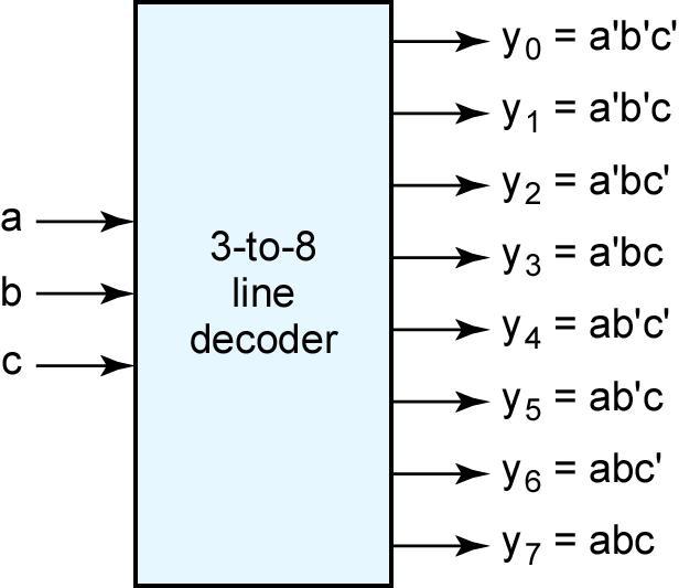
34 EXPERIMENT No. 7 Aim:- To Design a 3:8 Decoder using VHDL Decoder: A decoder is a device which does the reverse of an encoder, undoing the encoding so that the original information can be retrieved. The same method used to encode is usually just reversed in order to decode. In digital electronics, a decoder can take the form of a multiple-input, multipleoutput logic circuit that converts coded inputs into coded outputs, where the input and output codes are different. Decoding is necessary in applications such as data multiplexing, 7 segment display and memory address decoding. The truth table for 3:8 decoder and respective circuit diagram is as follows: Page34
35 Page35
36 Program: library ieee; use ieee.std_logic_1164.all; entity decoder_using_case is port ( enable :in std_logic; -- Enable for the decoder binary_in :in std_logic_vector (2 downto 0); -- 3-bit Input decoder_out :out std_logic_vector (7 downto 0) -- 8-bit Output ); end entity; architecture behavior of decoder_using_case is begin process (enable, binary_in) begin decoder_out <= X"000"; if (enable = '1') then case (binary_in) is when X"0" => decoder_out <= X"000"; when X"1" => decoder_out <= X"001"; when X"2" => decoder_out <= X"010"; when X"3" => decoder_out <= X"011"; when X"4" => decoder_out <= X"100"; when X"5" => decoder_out <= X"101"; when X"6" => decoder_out <= X"110"; when X"7" => decoder_out <= X"111"; end case; end if; end process; end architecture; OUTPUT: Page36

37 Simulation Waveform Quiz Questions with answer. Q.1 Name the examples of combinational logic circuits. Ans. Examples of common combinational logic circuits include: half adders, full adders, multiplexers, demultiplexers, encoders and decoders. Q.2 How many two-input AND and OR gates are required to realize Y=CD+EF+G? Ans Y=CD+EF+G Number of two input AND gates=2 Number of two input OR gates = 2 One OR gate to OR CD and EF and next to OR of G & output of first OR gate. Q.3 Which device converts BCD to Seven Segment? Ans. A device which converts BCD to Seven Segment is called DECODER. Q.4 What is a test bench in vhdl? Ans. A Test Bench in VHDL is code written in VHDL that provides stimulus for individual modules (also written in VHDL). Individual modules are instantiated by a single line of code showing the port. Q.5 What are the advantages of designing? Ans. Advantages of Designing: 1. Designing is useful in quick implementation, testing and useful in complex circuits. 2. Designing reduces the design cycle. Q6: Write the applications of Encoder and decoder. Ans: They are used in communication systems. Q7: Name some encoders. Ans Priority encoder, 4:2 encoder and etc. Q8: How many i/ps are in 4:2 encoder? Ans 4 i/ps and 2 o/ps. Q9: How many select lines are present in 2:4 decoder? Ans none Page37
38 EXPERIMENT No. 8 Aim:- To Design a 8 bit shift register 8-bit Shift Register Shift Register is a type of sequential circuit formed by combination of flip-flops and is capable of shifting data from left to right or vice-versa. Shift register basically performs two functions: i. Shifting of data(transfer of data) ii. Storage function The circuit diagram for 8-bit Shift Register is given as: The vhdl program for 8-bit shift-left register with a positive-edge clock, serial in, and serial out. Program: library ieee; use ieee.std_logic_1164.all; entity shift is port(c, SI : in std_logic; SO : out std_logic); end shift; architecture archi of shift is signal tmp: std_logic_vector(7 downto 0); begin process (C) begin if (C'event and C='1') then for i in 0 to 6 loop Page38

39 tmp(i+1) <= tmp(i); end loop; tmp(0) <= SI; end if; end process; SO <= tmp(7); end archi; Simulation Waveforms Quiz Questions with answer. Q.1 What is sequential logic? Ans. Sequential Logic: A logic circuit in which the outputs are a function of the present, and past inputs. The memory of past inputs involves the "state" of the system. At any time, if you know the present inputs, and state of the circuit, you can determine the outputs. Q.2 How many Flip-Flops are required for mod 16 counter? Ans. The number of flip-flops is required for Mod-16 Counter is 4. Q.3 A 4-bit synchronous counter uses flip-flops with propagation delay times of 15 ns each. How much maximum possible time required for change of state? Ans. 15 ns because in synchronous counter all the flip-flops change state at the same time. Q.4 How many flip flops are required to construct a decade counter? Ans. Decade counter counts 10 states from 0 to 9 ( i.e. from 0000 to 1001 ).Thus four Flip Flop's are required. Q.5 How many flip-flops are required to construct mod 30 counter? Ans 5 Q6: What is a flip flop? Ans. It is memory element which stores previous data. Page39
40 Q7: What is the function of clock in counter ckt? Ans: It synchronize the operation of flip flops in counter ckt. Q8: What is the maximum count for decade counter? Ans. From 0 to 9. Q9: What is down counter? Ans. When the qbar signal of previous ff is connected to clock of next ff. Q10. What is the count for decade down counter? Ans. From 9 to 0. Page40
41 EXPERIMENT No. 9 Aim:- To Design an arithmetic unit 4-bit Arithmetic Logic Unit The design and implementation of FPGA based Arithmetic Logic Unit is of core significance in digital technologies as it is an integral part of central processing unit. ALU is capable of calculating the results of a wide variety of basic arithmetical and logical computations. The ALU takes, as input, the data to be operated on (called operands) and a code, from the control unit, indicating which operation to perform. The output is the result of the computation. Designed ALU will perform the following operations: Arithmetic operations Bitwise logic operations All the modules described in the design are coded using VHDL which is a very useful tool with its degree of concurrency to cope with the parallelism of digital hardware. The block diagram for ALU is shown below: Block diagram of ALU Page41
42 There are two kinds of operation which an ALU can perform first part deals with arithmetic computations and is referred to as Arithmetic Unit. It is capable of addition, subtraction, multiplication, division, increment and decrement. The second part deals with the Gated results in the shape of AND, OR, XOR, inverter, rotate, left shift and right shift, which is referred to as Logic Unit. The functions are controlled and executed by selecting operation or control bits. Program: library IEEE; use IEEE.STD_LOGIC_1164.ALL; use IEEE.STD_LOGIC_ARITH.ALL; use IEEE.STD_LOGIC_UNSIGNED.ALL; entity alu is Port ( a : in STD_LOGIC_VECTOR (03 downto 0); b : in STD_LOGIC_VECTOR (03 downto 0); opcode : in STD_LOGIC_VECTOR (03 downto 0); y : out STD_LOGIC_VECTOR (03 downto 0)); end alu; Architecture Behavioral of alu is begin with opcode (3 downto 0) select y<= a when "0000", (not a) when "0001", b when "0010", (not b) when "0011", a and b when "0100", a or b when "0101", a nand b when "0110", a nor b when "0111", a xor b when "1000", a+1 when"1001", b+1 when "1010", a+b when "1011", a-1 when "1100", b-1 when "1101", a-b when "1110", a xnor b when "1111", "0000" when others; end Behavioral; Page42


43 RTL View Simulation Waveforms Quiz Questions with answer. Q.1 What is VHDL? Ans. VHDL is the VHSIC Hardware Description Language. VHSIC is an abbreviation for Very High Speed Integrated Circuit. Q.2 How many truth table entries are necessary for a four-input circuit? Ans. 16 Q.3 How many bits are there in BCD code? Ans. 4 Q.4 What is Combinational Logic? Ans. Combinational Logic: A logic circuit in which the outputs are a function of the inputs. At any time, if you know the inputs, you can determine the outputs. Q.5 What is stable state? Ans. Stable State: An internal or external signal maintains a constant magnitude Page43
44 (or specified range or function) for a period of time determined by external input signals. Q6. What is BCD to Gray converter? Ans: The converter which converts bcd code into gray code. Q7: What is the application of above code converter? Ans We use in communication systems. Q8. BCD to Gray converter is a combinational or sequential ckt? Ans. Combinational ckt. Q9: Write down the method of Binary to Gray conversion. Ans: Using the Ex-Or gates Q10: Convert 0101 to Decimal. Ans; 5 Page44
45 EXPERIMENT No. 10 Aim: implement ADC & DAC interface with FPGA The Spartan 3E Starter Kit provides us the basic features as provided by the Spartan 3E FPGA. It also provides easy way to test various programs in the FPGA itself, by dumping the bit file into the FPGA and then observing the output. The Spartan 3E FPGA board comes built in with many peripherals that help in the proper working of the board and also in interfacing the various signals to the board itself. ADCs (Analog to Digital Convertor) are of various types. The one used for our purpose is the Successive Approximation Type ADC (SAR-ADC), where the main components include a DAC (digital to analog convertor), a clock, a comparator and a SAR register for storing the values of the digital data which comes after the comparator compares the values of the DAC with the analog input and outputs a 1 or a 0 depending on the condition. Block diagram of SAR- ADC Page45
46 Circuit Diagram of the LTC1407A ADC chip Working of ADC ADC presents a 14-bit, 2 s complement digital output of the analog input. The input voltage given to the ADC depends on the programmable gain settings of the preamplifier. The maximum input range is for the gain = -1 for which the input voltage range from 0.4V to 2.9V. The Analog to Digital Conversion formula is given below: Here D [13:0] represents the 14 bit two s complement value of the analog input. It is output to the FPGA from the ADC via the SPI_MISO signal, as will be discussed later in the interfacing signals of the FPGA and the ADC. GAIN is the gain setting given via the programming of the gain register bit by bit. VIN is the input voltage to the ADC. 1.65V is the reference voltage of the ADC. This is achieved by the voltage divider circuit provided in the ADC circuit (dividing the Vcc which is 3.3V). The range of the ADC used is ±1.25V. Hence the output is scaled by 1.25V. Also the output obtained is in 14 bit 2 s complement form and hence the output is scaled by Both the input channels [VIN(A) and VIN(B)] are sampled simultaneously. Communication Between FPGA and ADC o AD_CONV: This signal is active high shutdown and reset signal. This signal marks the beginning of the conversion of the analog signal. It is an internal signal of the FPGA board, which can t be viewed with the help of an external oscilloscope. Pin P11 is responsible for this signal. This signal is directed from FPGA to ADC. o SPI_MISO: This signal is the serial data output from the ADC chip to the FPGA board. It is the one that gives the digital representation of the sampled analog value as 14-bit 2 s complement binary value. It is again an internal signal and pin N10 is responsible for this signal. This signal is directed from FPGA to ADC. Page46
47 o SPI_SCK: As described earlier, this is the clock signal which plays an important role in the analog to digital conversion process and also sending the data from the ADC unit to the FPGA. Serial interface timing diagram for ADC conversion and sampling The Spartan-3E Starter Kit board includes an SPI-compatible, four-channel, serial Digital to-analog Converter (DAC). The DAC device is a Linear Technology LTC2624 quad DAC with 12-bit unsigned resolution. SPI Communication The FPGA uses a Serial Peripheral Interface (SPI) to send digital values to each of the four DAC channels. The SPI bus is a full-duplex, synchronous, character-oriented channel employing a simple four-wire interface. The interface signals between the FPGA and the DAC are the SPI_MOSI, SPI_MISO, and SPI_SCK which are shared with the other devices on the SPI bus. The DAC_CS signal is the active-low slave select input to the DAC. The DAC_CLR signal is the active-low, asynchronous reset input to the DAC. As a bus master the FPGA drives the bus clock signal (SPI_SCK) and transmits serial data (SPI_MOSI) to the selected DAC bus slave (Xilinx,2006). WORKING PRINCIPLE This system produces analog voltage at the output of DAC according to the digital value provided by the FPGA. The digital input of the DAC is controlled with the help of rotary switch. The rotation of switch in clockwise direction increase the analog output value and rotation in anticlockwise direction result in the decrement of the analog output value. The step voltage of increment is controlled with a pushbutton switch. Default step voltage is 100mv. With pressing this switch we can change the step from 100mv to 10mv. For the next push it switches to previous state. RESULT ANALYSIS Page47

. Individual modules are instantiated by a single line of code showing the port. Q.")
48 The developed VHDL code has been implemented on the Spartan-3E starter kit. The design is synthesized and implemented on the FPGA by using the Xilinx ISE 13.2 software. Conclusion The ADC was analyzed for a constant voltage supply. The onboard ADC of the Spartan 3E Starter Kit FPGA Board was properly interfaced with real world signals. Quiz Questions with answer. Q.1 Who is the father of VHDL? Ans. John Hines, Wright Patterson AFB, Daton Ohio. Q.2 What is a testbench in vhdl? Ans.A Test Bench in VHDL is code written in VHDL that provides stimulus for individual modules (also written in VHDL). Individual modules are instantiated by a single line of code showing the port. Q.3 How many inputs and output are used in Full adder? Ans. Three inputs and two output. Q.4 What are the advantages of designing? Ans. Advantages of Designing: 1. Designing is useful in quick implementation, testing and useful in complex circuits. 2. Designing reduces the design cycle. Q.5 Why HDL is used? Page48
49 Ans. HDL is used because it is easy to design, implement, test and document increasingly complex digital system. Q6. Give the basic rules for binary addition? Ans. 0+0 = 0; 0+1 = 1 ; 1+1 = 1 0 ; 1+0 = 1. Q7: What is the drawback of half adder? Ans: We can t add carry bit from previous stage. Q8: What is the difference b/w half adder& half sub tractor? Ans: Half adder can add two bits & half sub tractor can subtract two bits. Q9: Define Nibble? Ans. Combination of four bits Page49
50 EXPERIMENT No. 11 Aim:-Implement a serial communication interface with FPGA The Serial Peripheral Interface (SPI) is a high speed (up to 400 Mhz) synchronous serial interface/protocol designed by Motorola. It is a popular interface used for connecting peripherals to each other and to microprocessors. Most literature indicates that the interface can only be used for eight or sixteen bit block data transfers, but many Motorola microcontrollers allow transfers of any range of blocks between two and sixteen bits at a time. Because of the serial nature of the interface, data transfers of more than sixteen bits at a time can be implemented easily through control signals. There are four possibilities for clocking the data based on the clock polarity and the clock phase: Data transfer Conclusion: Complete coding of SPI Protocol using VHDL can be implemented on FPGA XC3S400. Quiz Questions with answer. Q.1 Who is the father of VHDL? Ans. John Hines, Wright Patterson AFB, Daton Ohio. Q.2 What is a testbench in vhdl? Ans.A Test Bench in VHDL is code written in VHDL that provides stimulus for individual modules (also written in VHDL). Individual modules are instantiated by a single line of code showing the port. Q.3 How many inputs and output are used in Full adder? Page50
51 Ans. Three inputs and two output. Q.4 What are the advantages of designing? Ans. Advantages of Designing: 1. Designing is useful in quick implementation, testing and useful in complex circuits. 2. Designing reduces the design cycle. Q.5 Why HDL is used? Ans. HDL is used because it is easy to design, implement, test and document increasingly complex digital system. Q6. Give the basic rules for binary addition? Ans. 0+0 = 0; 0+1 = 1 ; 1+1 = 1 0 ; 1+0 = 1. Q7: What is the drawback of half adder? Ans: We can t add carry bit from previous stage. Q8: What is the difference b/w half adder& half sub tractor? Ans: Half adder can add two bits & half sub tractor can subtract two bits. Q9: Define Nibble? Ans. Combination of four bits Page51
MODULE 3. Combinational & Sequential logic
 MODULE 3 Combinational & Sequential logic Combinational Logic Introduction Logic circuit may be classified into two categories. Combinational logic circuits 2. Sequential logic circuits A combinational
WINTER 15 EXAMINATION Model Answer
 Important Instructions to examiners: 1) The answers should be examined by key words and not as word-to-word as given in the model answer scheme. 2) The model answer and the answer written by candidate
Logic Design Viva Question Bank Compiled By Channveer Patil
 Logic Design Viva Question Bank Compiled By Channveer Patil Title of the Practical: Verify the truth table of logic gates AND, OR, NOT, NAND and NOR gates/ Design Basic Gates Using NAND/NOR gates. Q.1
Microprocessor Design
 Microprocessor Design Principles and Practices With VHDL Enoch O. Hwang Brooks / Cole 2004 To my wife and children Windy, Jonathan and Michelle Contents 1. Designing a Microprocessor... 2 1.1 Overview
Contents Circuits... 1
 Contents Circuits... 1 Categories of Circuits... 1 Description of the operations of circuits... 2 Classification of Combinational Logic... 2 1. Adder... 3 2. Decoder:... 3 Memory Address Decoder... 5 Encoder...
R13 SET - 1 '' ''' '' ' '''' Code No: RT21053
 SET - 1 1. a) What are the characteristics of 2 s complement numbers? b) State the purpose of reducing the switching functions to minimal form. c) Define half adder. d) What are the basic operations in
 UNIT 1 NUMBER SYSTEMS AND DIGITAL LOGIC FAMILIES 1. Briefly explain the stream lined method of converting binary to decimal number with example. 2. Give the Gray code for the binary number (111) 2. 3.
AIM: To study and verify the truth table of logic gates
 EXPERIMENT: 1- LOGIC GATES AIM: To study and verify the truth table of logic gates LEARNING OBJECTIVE: Identify various Logic gates and their output. COMPONENTS REQUIRED: KL-31001 Digital Logic Lab( Main
ACS College of Engineering. Department of Biomedical Engineering. HDL pre lab questions ( ) Cycle-1
 Cycle-1") ACS College of Engineering Department of Biomedical Engineering HDL pre lab questions (2015-2016) Cycle-1 1. What is truth table? 2. Which gates are called universal gates? 3. Define HDL? 4. What is the
ACS College of Engineering Department of Biomedical Engineering HDL pre lab questions (2015-2016) Cycle-1 1. What is truth table? 2. Which gates are called universal gates? 3. Define HDL? 4. What is the
DEPARTMENT OF COMPUTER SCIENCE & ENGINEERING
 DRONACHARYA GROUP OF INSTITUTIONS, GREATER NOIDA Affiliated to Mahamaya Technical University, Noida Approved by AICTE DEPARTMENT OF COMPUTER SCIENCE & ENGINEERING Lab Manual for Computer Organization Lab
Dev Bhoomi Institute Of Technology Department of Electronics and Communication Engineering PRACTICAL INSTRUCTION SHEET
 Dev Bhoomi Institute Of Technology Department of Electronics and Communication Engineering PRACTICAL INSTRUCTION SHEET LABORATORY MANUAL EXPERIMENT NO. 1 ISSUE NO. : ISSUE DATE: REV. NO. : REV. DATE :
DIGITAL SYSTEM DESIGN UNIT I (2 MARKS)
") DIGITAL SYSTEM DESIGN UNIT I (2 MARKS) 1. Convert Binary number (111101100) 2 to Octal equivalent. 2. Convert Binary (1101100010011011) 2 to Hexadecimal equivalent. 3. Simplify the following Boolean function
DIGITAL SYSTEM DESIGN UNIT I (2 MARKS) 1. Convert Binary number (111101100) 2 to Octal equivalent. 2. Convert Binary (1101100010011011) 2 to Hexadecimal equivalent. 3. Simplify the following Boolean function
MODU LE DAY. Class-A, B, AB and C amplifiers - basic concepts, power, efficiency Basic concepts of Feedback and Oscillation. Day 1
 DAY MODU LE TOPIC QUESTIONS Day 1 Day 2 Day 3 Day 4 I Class-A, B, AB and C amplifiers - basic concepts, power, efficiency Basic concepts of Feedback and Oscillation Phase Shift Wein Bridge oscillators.
Analogue Versus Digital [5 M]
![Analogue Versus Digital [5 M]](/thumbs/93/111640168.jpg "Analogue Versus Digital [5 M]") Q.1 a. Analogue Versus Digital [5 M] There are two basic ways of representing the numerical values of the various physical quantities with which we constantly deal in our day-to-day lives. One of the ways,
Q.1 a. Analogue Versus Digital [5 M] There are two basic ways of representing the numerical values of the various physical quantities with which we constantly deal in our day-to-day lives. One of the ways,
QUICK GUIDE COMPUTER LOGICAL ORGANIZATION - OVERVIEW
 QUICK GUIDE http://www.tutorialspoint.com/computer_logical_organization/computer_logical_organization_quick_guide.htm COMPUTER LOGICAL ORGANIZATION - OVERVIEW Copyright tutorialspoint.com In the modern
MODEL QUESTIONS WITH ANSWERS THIRD SEMESTER B.TECH DEGREE EXAMINATION DECEMBER CS 203: Switching Theory and Logic Design. Time: 3 Hrs Marks: 100
 MODEL QUESTIONS WITH ANSWERS THIRD SEMESTER B.TECH DEGREE EXAMINATION DECEMBER 2016 CS 203: Switching Theory and Logic Design Time: 3 Hrs Marks: 100 PART A ( Answer All Questions Each carries 3 Marks )
R13. II B. Tech I Semester Regular Examinations, Jan DIGITAL LOGIC DESIGN (Com. to CSE, IT) PART-A
 PART-A") SET - 1 Note: Question Paper consists of two parts (Part-A and Part-B) Answer ALL the question in Part-A Answer any THREE Questions from Part-B a) What are the characteristics of 2 s complement numbers?
SET - 1 Note: Question Paper consists of two parts (Part-A and Part-B) Answer ALL the question in Part-A Answer any THREE Questions from Part-B a) What are the characteristics of 2 s complement numbers?
PHYSICS 5620 LAB 9 Basic Digital Circuits and Flip-Flops
 PHYSICS 5620 LAB 9 Basic Digital Circuits and Flip-Flops Objective Construct a two-bit binary decoder. Study multiplexers (MUX) and demultiplexers (DEMUX). Construct an RS flip-flop from discrete gates.
Laboratory Objectives and outcomes for Digital Design Lab
 Class: SE Department of Information Technology Subject Logic Design Sem : III Course Objectives and outcomes for LD Course Objectives: Students will try to : COB1 Understand concept of various components.
Dev Bhoomi Institute Of Technology PRACTICAL INSTRUCTION SHEET EXPERIMENT NO. ISSUE NO. : ISSUE DATE: REV. NO. : REV. DATE : PAGE:
 Dev Bhoomi Institute Of Technology LABORATORY MANUAL PRACTICAL INSTRUCTION SHEET EXPERIMENT NO. ISSUE NO. : ISSUE DATE: REV. NO. : REV. DATE : PAGE: LABORATORY Name & Code: Digital Electronics SEMESTER:
HDL & High Level Synthesize (EEET 2035) Laboratory II Sequential Circuits with VHDL: DFF, Counter, TFF and Timer
 Laboratory II Sequential Circuits with VHDL: DFF, Counter, TFF and Timer") 1 P a g e HDL & High Level Synthesize (EEET 2035) Laboratory II Sequential Circuits with VHDL: DFF, Counter, TFF and Timer Objectives: Develop the behavioural style VHDL code for D-Flip Flop using gated,
1 P a g e HDL & High Level Synthesize (EEET 2035) Laboratory II Sequential Circuits with VHDL: DFF, Counter, TFF and Timer Objectives: Develop the behavioural style VHDL code for D-Flip Flop using gated,
Find the equivalent decimal value for the given value Other number system to decimal ( Sample)
") VELAMMAL COLLEGE OF ENGINEERING AND TECHNOLOGY, MADURAI 65 009 Department of Information Technology Model Exam-II-Question bank PART A (Answer for all Questions) (8 X = 6) K CO Marks Find the equivalent
VELAMMAL COLLEGE OF ENGINEERING AND TECHNOLOGY, MADURAI 65 009 Department of Information Technology Model Exam-II-Question bank PART A (Answer for all Questions) (8 X = 6) K CO Marks Find the equivalent
MAHARASHTRA STATE BOARD OF TECHNICAL EDUCATION (Autonomous) (ISO/IEC Certified) WINTER 2018 EXAMINATION MODEL ANSWER
 (ISO/IEC Certified) WINTER 2018 EXAMINATION MODEL ANSWER") Important Instructions to examiners: 1) The answers should be examined by key words and not as word-to-word as given in themodel answer scheme. 2) The model answer and the answer written by candidate may
Important Instructions to examiners: 1) The answers should be examined by key words and not as word-to-word as given in themodel answer scheme. 2) The model answer and the answer written by candidate may
Solution to Digital Logic )What is the magnitude comparator? Design a logic circuit for 4 bit magnitude comparator and explain it,
What is the magnitude comparator? Design a logic circuit for 4 bit magnitude comparator and explain it,") Solution to Digital Logic -2067 Solution to digital logic 2067 1.)What is the magnitude comparator? Design a logic circuit for 4 bit magnitude comparator and explain it, A Magnitude comparator is a combinational
Solution to Digital Logic -2067 Solution to digital logic 2067 1.)What is the magnitude comparator? Design a logic circuit for 4 bit magnitude comparator and explain it, A Magnitude comparator is a combinational
MUHAMMAD NAEEM LATIF MCS 3 RD SEMESTER KHANEWAL
 1. A stage in a shift register consists of (a) a latch (b) a flip-flop (c) a byte of storage (d) from bits of storage 2. To serially shift a byte of data into a shift register, there must be (a) one click
ECE 263 Digital Systems, Fall 2015
 ECE 263 Digital Systems, Fall 2015 REVIEW: FINALS MEMORY ROM, PROM, EPROM, EEPROM, FLASH RAM, DRAM, SRAM Design of a memory cell 1. Draw circuits and write 2 differences and 2 similarities between DRAM
CS6201 UNIT I PART-A. Develop or build the following Boolean function with NAND gate F(x,y,z)=(1,2,3,5,7).
=(1,2,3,5,7).") VALLIAMMAI ENGINEERING COLLEGE SRM Nagar, Kattankulathur-603203 DEPARTMENT OF COMPUTER SCIENCE AND ENGINEERING Academic Year: 2015-16 BANK - EVEN SEMESTER UNIT I PART-A 1 Find the octal equivalent of hexadecimal
VALLIAMMAI ENGINEERING COLLEGE SRM Nagar, Kattankulathur-603203 DEPARTMENT OF COMPUTER SCIENCE AND ENGINEERING Academic Year: 2015-16 BANK - EVEN SEMESTER UNIT I PART-A 1 Find the octal equivalent of hexadecimal
Tribhuvan University Institute of Science and Technology Bachelor of Science in Computer Science and Information Technology
 Tribhuvan University Institute of Science and Technology Bachelor of Science in Computer Science and Information Technology Course Title: Digital Logic Full Marks: 60 + 0 + 0 Course No.: CSC Pass Marks:
TIME SCHEDULE. MODULE TOPICS PERIODS 1 Number system & Boolean algebra 17 Test I 1 2 Logic families &Combinational logic
 COURSE TITLE : DIGITAL INSTRUMENTS PRINCIPLE COURSE CODE : 3075 COURSE CATEGORY : B PERIODS/WEEK : 4 PERIODS/SEMESTER : 72 CREDITS : 4 TIME SCHEDULE MODULE TOPICS PERIODS 1 Number system & Boolean algebra
WINTER 14 EXAMINATION
 Subject Code: 17320 WINTER 14 EXAMINATION Model Answer Important Instructions to examiners: 1) The answers should be examined by key words and not as word-to-word as given in the model answer scheme. 2)
CS302 Digital Logic Design Solved Objective Midterm Papers For Preparation of Midterm Exam
 CS302 Digital Logic Design Solved Objective Midterm Papers For Preparation of Midterm Exam MIDTERM EXAMINATION Spring 2012 Question No: 1 ( Marks: 1 ) - Please choose one A SOP expression is equal to 1
1. Convert the decimal number to binary, octal, and hexadecimal.
 1. Convert the decimal number 435.64 to binary, octal, and hexadecimal. 2. Part A. Convert the circuit below into NAND gates. Insert or remove inverters as necessary. Part B. What is the propagation delay
Department of Computer Science and Engineering Question Bank- Even Semester:
 Department of Computer Science and Engineering Question Bank- Even Semester: 2014-2015 CS6201& DIGITAL PRINCIPLES AND SYSTEM DESIGN (Common to IT & CSE, Regulation 2013) UNIT-I 1. Convert the following
Chapter 4. Logic Design
 Chapter 4 Logic Design 4.1 Introduction. In previous Chapter we studied gates and combinational circuits, which made by gates (AND, OR, NOT etc.). That can be represented by circuit diagram, truth table
Flip Flop. S-R Flip Flop. Sequential Circuits. Block diagram. Prepared by:- Anwar Bari
 Sequential Circuits The combinational circuit does not use any memory. Hence the previous state of input does not have any effect on the present state of the circuit. But sequential circuit has memory
Bachelor Level/ First Year/ Second Semester/ Science Full Marks: 60 Computer Science and Information Technology (CSc. 151) Pass Marks: 24
 Pass Marks: 24") 2065 Computer Science and Information Technology (CSc. 151) Pass Marks: 24 Time: 3 hours. Candidates are required to give their answers in their own words as for as practicable. Attempt any TWO questions:
2065 Computer Science and Information Technology (CSc. 151) Pass Marks: 24 Time: 3 hours. Candidates are required to give their answers in their own words as for as practicable. Attempt any TWO questions:
PURBANCHAL UNIVERSITY
 [c] Implement a full adder circuit with a decoder and two OR gates. [4] III SEMESTER FINAL EXAMINATION-2006 Q. [4] [a] What is flip flop? Explain flip flop operating characteristics. [6] [b] Design and
EXPERIMENT: 1. Graphic Symbol: OR: The output of OR gate is true when one of the inputs A and B or both the inputs are true.
 EXPERIMENT: 1 DATE: VERIFICATION OF BASIC LOGIC GATES AIM: To verify the truth tables of Basic Logic Gates NOT, OR, AND, NAND, NOR, Ex-OR and Ex-NOR. APPARATUS: mention the required IC numbers, Connecting
Advanced Devices. Registers Counters Multiplexers Decoders Adders. CSC258 Lecture Slides Steve Engels, 2006 Slide 1 of 20
 Advanced Devices Using a combination of gates and flip-flops, we can construct more sophisticated logical devices. These devices, while more complex, are still considered fundamental to basic logic design.
MODULAR DIGITAL ELECTRONICS TRAINING SYSTEM
 MODULAR DIGITAL ELECTRONICS TRAINING SYSTEM MDETS UCTECH's Modular Digital Electronics Training System is a modular course covering the fundamentals, concepts, theory and applications of digital electronics.
S.K.P. Engineering College, Tiruvannamalai UNIT I
 UNIT I NUMBER SYSTEMS AND DIGITAL LOGIC FAMILIES Part - A Questions 1. Convert the hexadecimal number E3FA to binary.( Nov 2007) E3FA 16 Hexadecimal E 3 F A 11102 00112 11112 10102 So the equivalent binary
Introduction to Digital Logic Missouri S&T University CPE 2210 Exam 3 Logistics
 Introduction to Digital Logic Missouri S&T University CPE 2210 Exam 3 Logistics Egemen K. Çetinkaya Egemen K. Çetinkaya Department of Electrical & Computer Engineering Missouri University of Science and
Subject : EE6301 DIGITAL LOGIC CIRCUITS
 QUESTION BANK Programme : BE Subject : Semester / Branch : III/EEE UNIT 1 NUMBER SYSTEMS AND DIGITAL LOGIC FAMILIES Review of number systems, binary codes, error detection and correction codes (Parity
DepartmentofElectronicEngineering NEDUniversity ofengineering &Technology LABORATORY WORKBOOK DIGITAL LOGIC DESIGN (TC-201)
") DepartmentofElectronicEngineering NEDUniversity ofengineering &Technology LABORATORY WORKBOOK DIGITAL LOGIC DESIGN (TC-201) Instructor Name: Student Name: Roll Number: Semester: Batch: Year: Department:
DepartmentofElectronicEngineering NEDUniversity ofengineering &Technology LABORATORY WORKBOOK DIGITAL LOGIC DESIGN (TC-201) Instructor Name: Student Name: Roll Number: Semester: Batch: Year: Department:
Final Exam review: chapter 4 and 5. Supplement 3 and 4
 Final Exam review: chapter 4 and 5. Supplement 3 and 4 1. A new type of synchronous flip-flop has the following characteristic table. Find the corresponding excitation table with don t cares used as much
Principles of Computer Architecture. Appendix A: Digital Logic
 A-1 Appendix A - Digital Logic Principles of Computer Architecture Miles Murdocca and Vincent Heuring Appendix A: Digital Logic A-2 Appendix A - Digital Logic Chapter Contents A.1 Introduction A.2 Combinational
Logic Devices for Interfacing, The 8085 MPU Lecture 4
 Logic Devices for Interfacing, The 8085 MPU Lecture 4 1 Logic Devices for Interfacing Tri-State devices Buffer Bidirectional Buffer Decoder Encoder D Flip Flop :Latch and Clocked 2 Tri-state Logic Outputs
Computer Architecture and Organization
 A-1 Appendix A - Digital Logic Computer Architecture and Organization Miles Murdocca and Vincent Heuring Appendix A Digital Logic A-2 Appendix A - Digital Logic Chapter Contents A.1 Introduction A.2 Combinational
Experiment 8 Introduction to Latches and Flip-Flops and registers
 Experiment 8 Introduction to Latches and Flip-Flops and registers Introduction: The logic circuits that have been used until now were combinational logic circuits since the output of the device depends
Introduction to Digital Electronics
 Introduction to Digital Electronics by Agner Fog, 2018-10-15. Contents 1. Number systems... 3 1.1. Decimal, binary, and hexadecimal numbers... 3 1.2. Conversion from another number system to decimal...
TYPICAL QUESTIONS & ANSWERS
 DIGITALS ELECTRONICS TYPICAL QUESTIONS & ANSWERS OBJECTIVE TYPE QUESTIONS Each Question carries 2 marks. Choose correct or the best alternative in the following: Q.1 The NAND gate output will be low if
St. MARTIN S ENGINEERING COLLEGE
 St. MARTIN S ENGINEERING COLLEGE Dhulapally, Kompally, Secunderabad-500014. Branch Year&Sem Subject Name : Electronics and Communication Engineering : II B. Tech I Semester : SWITCHING THEORY AND LOGIC
SEQUENTIAL LOGIC. Satish Chandra Assistant Professor Department of Physics P P N College, Kanpur
 SEQUENTIAL LOGIC Satish Chandra Assistant Professor Department of Physics P P N College, Kanpur www.satish0402.weebly.com OSCILLATORS Oscillators is an amplifier which derives its input from output. Oscillators
North Shore Community College
 North Shore Community College Course Number: IEL217 Section: MAL Course Name: Digital Electronics 1 Semester: Credit: 4 Hours: Three hours of Lecture, Two hours Laboratory per week Thursdays 8:00am (See
Outline. CPE/EE 422/522 Advanced Logic Design L04. Review: 8421 BCD to Excess3 BCD Code Converter. Review: Mealy Sequential Networks
 Outline PE/EE 422/522 Advanced Logic Design L4 Electrical and omputer Engineering University of Alabama in Huntsville What we know ombinational Networks Analysis, Synthesis, Simplification, Hazards, Building
Electrical and Telecommunications Engineering Technology_TCET3122/TC520. NEW YORK CITY COLLEGE OF TECHNOLOGY The City University of New York
 NEW YORK CITY COLLEGE OF TECHNOLOGY The City University of New York DEPARTMENT: SUBJECT CODE AND TITLE: COURSE DESCRIPTION: REQUIRED: Electrical and Telecommunications Engineering Technology TCET 3122/TC
CHAPTER 4: Logic Circuits
 CHAPTER 4: Logic Circuits II. Sequential Circuits Combinational circuits o The outputs depend only on the current input values o It uses only logic gates, decoders, multiplexers, ALUs Sequential circuits
UNIT III. Combinational Circuit- Block Diagram. Sequential Circuit- Block Diagram
 UNIT III INTRODUCTION In combinational logic circuits, the outputs at any instant of time depend only on the input signals present at that time. For a change in input, the output occurs immediately. Combinational
Objectives. Combinational logics Sequential logics Finite state machine Arithmetic circuits Datapath
 Objectives Combinational logics Sequential logics Finite state machine Arithmetic circuits Datapath In the previous chapters we have studied how to develop a specification from a given application, and
Vignana Bharathi Institute of Technology UNIT 4 DLD
 DLD UNIT IV Synchronous Sequential Circuits, Latches, Flip-flops, analysis of clocked sequential circuits, Registers, Shift registers, Ripple counters, Synchronous counters, other counters. Asynchronous
Chapter Contents. Appendix A: Digital Logic. Some Definitions
 A- Appendix A - Digital Logic A-2 Appendix A - Digital Logic Chapter Contents Principles of Computer Architecture Miles Murdocca and Vincent Heuring Appendix A: Digital Logic A. Introduction A.2 Combinational
CHAPTER 4: Logic Circuits
 CHAPTER 4: Logic Circuits II. Sequential Circuits Combinational circuits o The outputs depend only on the current input values o It uses only logic gates, decoders, multiplexers, ALUs Sequential circuits
IT T35 Digital system desigm y - ii /s - iii
 UNIT - III Sequential Logic I Sequential circuits: latches flip flops analysis of clocked sequential circuits state reduction and assignments Registers and Counters: Registers shift registers ripple counters
EEE130 Digital Electronics I Lecture #1_2. Dr. Shahrel A. Suandi
 EEE130 Digital Electronics I Lecture #1_2 Dr. Shahrel A. Suandi 1-4 Overview of Basic Logic Functions Digital systems are generally built from combinations of NOT, AND and OR logic elements The combinations
Flip-flop and Registers
 ECE 322 Digital Design with VHDL Flip-flop and Registers Lecture Textbook References n Sequential Logic Review Stephen Brown and Zvonko Vranesic, Fundamentals of Digital Logic with VHDL Design, 2 nd or
Chapter 3 Unit Combinational
 EE 200: Digital Logic Circuit Design Dr Radwan E Abdel-Aal, COE Logic and Computer Design Fundamentals Chapter 3 Unit Combinational 5 Registers Logic and Design Counters Part Implementation Technology
UNIVERSITI TEKNOLOGI MALAYSIA
 SULIT Faculty of Computing UNIVERSITI TEKNOLOGI MALAYSIA FINAL EXAMINATION SEMESTER I, 2016 / 2017 SUBJECT CODE : SUBJECT NAME : SECTION : TIME : DATE/DAY : VENUES : INSTRUCTIONS : Answer all questions
DIGITAL SYSTEM FUNDAMENTALS (ECE421) DIGITAL ELECTRONICS FUNDAMENTAL (ECE422) COUNTERS
 DIGITAL ELECTRONICS FUNDAMENTAL (ECE422) COUNTERS") COURSE / CODE DIGITAL SYSTEM FUNDAMENTALS (ECE421) DIGITAL ELECTRONICS FUNDAMENTAL (ECE422) COUNTERS One common requirement in digital circuits is counting, both forward and backward. Digital clocks and
COURSE / CODE DIGITAL SYSTEM FUNDAMENTALS (ECE421) DIGITAL ELECTRONICS FUNDAMENTAL (ECE422) COUNTERS One common requirement in digital circuits is counting, both forward and backward. Digital clocks and
TRAINING KITS ON DIGITAL ELECTRONIC EXPERIMENTS. Verify Truth table for TTL IC s AND, NOT, & NAND GATES
 TRAINING KITS ON DIGITAL ELECTRONIC EXPERIMENTS CEE 2800 Basic Logic Gates using TTL IC's (7 in 1) To verify the truth table For TTL AND, OR. NOT, NAND,NOR, EX-OR, & EX-NOR Gates. Instrument comprises
Chapter 8 Functions of Combinational Logic
 ETEC 23 Programmable Logic Devices Chapter 8 Functions of Combinational Logic Shawnee State University Department of Industrial and Engineering Technologies Copyright 27 by Janna B. Gallaher Basic Adders
MASSACHUSETTS INSTITUTE OF TECHNOLOGY Department of Electrical Engineering and Computer Sciences
 MASSACHUSETTS INSTITUTE OF TECHNOLOGY Department of Electrical Engineering and Computer Sciences Introductory Digital Systems Lab (6.111) Quiz #2 - Spring 2003 Prof. Anantha Chandrakasan and Prof. Don
DIGITAL ELECTRONICS LAB MANUAL FOR 2/4 B.Tech (ECE) COURSE CODE: EC-252
 COURSE CODE: EC-252") DIGITAL ELECTRONICS LAB MANUAL FOR /4 B.Tech (ECE) COURSE CODE: EC-5 PREPARED BY P.SURENDRA KUMAR M.TECH, Lecturer D.SWETHA M.TECH, Lecturer T Srinivasa Rao M.TECH, Lecturer Ch.Madhavi, Lab Assistant 009-00
DIGITAL ELECTRONICS LAB MANUAL FOR /4 B.Tech (ECE) COURSE CODE: EC-5 PREPARED BY P.SURENDRA KUMAR M.TECH, Lecturer D.SWETHA M.TECH, Lecturer T Srinivasa Rao M.TECH, Lecturer Ch.Madhavi, Lab Assistant 009-00
MAHARASHTRA STATE BOARD OF TECHNICAL EDUCATION (Autonomous) (ISO/IEC Certified)
 (ISO/IEC Certified)") Important Instructions to examiners: 1) The answers should be examined by key words and not as word-to-word as given in the model answer scheme. 2) The model answer and the answer written by candidate
Important Instructions to examiners: 1) The answers should be examined by key words and not as word-to-word as given in the model answer scheme. 2) The model answer and the answer written by candidate
Decade Counters Mod-5 counter: Decade Counter:
 Decade Counters We can design a decade counter using cascade of mod-5 and mod-2 counters. Mod-2 counter is just a single flip-flop with the two stable states as 0 and 1. Mod-5 counter: A typical mod-5
1 Hour Sample Test Papers: Sample Test Paper 1. Roll No.
 6.1.2 Sample Test Papers: Sample Test Paper 1 Roll No. Institute Name: Course Code: EJ/EN/ET/EX/EV/IC/IE/IS/MU/DE/ED/ET/IU Subject: Principles of Digital Techniques Marks: 25 1 Hour 1. All questions are
DIGITAL CIRCUIT LOGIC UNIT 9: MULTIPLEXERS, DECODERS, AND PROGRAMMABLE LOGIC DEVICES
 DIGITAL CIRCUIT LOGIC UNIT 9: MULTIPLEXERS, DECODERS, AND PROGRAMMABLE LOGIC DEVICES 1 Learning Objectives 1. Explain the function of a multiplexer. Implement a multiplexer using gates. 2. Explain the
Logic Design. Flip Flops, Registers and Counters
 Logic Design Flip Flops, Registers and Counters Introduction Combinational circuits: value of each output depends only on the values of inputs Sequential Circuits: values of outputs depend on inputs and
NORTHWESTERN UNIVERSITY TECHNOLOGICAL INSTITUTE
 NORTHWESTERN UNIVERSITY TECHNOLOGICL INSTITUTE ECE 270 Experiment #8 DIGITL CIRCUITS Prelab 1. Draw the truth table for the S-R Flip-Flop as shown in the textbook. Draw the truth table for Figure 7. 2.
EE 210. LOGIC DESIGN LAB.
 College of Engineering Electrical Engineering Department EE 210. LOGIC DESIGN LAB. (1 st semester 1426-27) Dr. Messaoud Boukezzata Office: EE 11 Phone: 063 8000 50 Ext 3152 1 College of Engineering Electrical
Jawaharlal Nehru Engineering College
 Jawaharlal Nehru Engineering College Laboratory Manual DIGITAL LOGIC DESIGN For Second Year Students Manual made by Dr. V. A. More Author JNEC, Aurangabad MGM S Jawaharlal Nehru Engineering College N-6,
MAHARASHTRA STATE BOARD OF TECHNICAL EDUCATION (Autonomous)
") Subject Code: 17320 Model Answer Page 1 of 32 Important Instructions to examiners: 1) The answers should be examined by key words and not as word-to-word as given in the Model answer scheme. 2) The model
Subject Code: 17320 Model Answer Page 1 of 32 Important Instructions to examiners: 1) The answers should be examined by key words and not as word-to-word as given in the Model answer scheme. 2) The model
DIGITAL CIRCUIT COMBINATORIAL LOGIC
 DIGITAL CIRCUIT COMBINATORIAL LOGIC Logic levels: one zero true false high low CMOS logic levels: 1 => 0.7 V DD 0.4 V DD = noise margin 0 =< 0.3 V DD Positive logic: high = 1 = true low = 0 = false Negative
Vivekananda College of Engineering and Technology Puttur (D.K)
") Vivekananda College of Engineering and Technology Puttur (D.K) Analog and Digital Electronics Laboratory Manual 5CSL 37 Author Prof. Mahesh Prasanna K Assoc. Professor & Head, CSE kmpshastry@gmail.com
Vivekananda College of Engineering and Technology Puttur (D.K) Analog and Digital Electronics Laboratory Manual 5CSL 37 Author Prof. Mahesh Prasanna K Assoc. Professor & Head, CSE kmpshastry@gmail.com
Inside Digital Design Accompany Lab Manual
 1 Inside Digital Design, Accompany Lab Manual Inside Digital Design Accompany Lab Manual Simulation Prototyping Synthesis and Post Synthesis Name- Roll Number- Total/Obtained Marks- Instructor Signature-
Bachelor of Technology (Electronics and Instrumentation Engg.)
") 1 A Project Report on Embedded processor design and Implementation of CAM In partial fulfillment of the requirements of Bachelor of Technology (Electronics and Instrumentation Engg.) Submitted By Jaswant
1 A Project Report on Embedded processor design and Implementation of CAM In partial fulfillment of the requirements of Bachelor of Technology (Electronics and Instrumentation Engg.) Submitted By Jaswant
[2 credit course- 3 hours per week]
![[2 credit course- 3 hours per week]](/thumbs/94/121292011.jpg "[2 credit course- 3 hours per week]") Syllabus of Applied Electronics for F Y B Sc Semester- 1 (With effect from June 2012) PAPER I: Components and Devices [2 credit course- 3 hours per week] Unit- I : CIRCUIT THEORY [10 Hrs] Introduction;
Syllabus of Applied Electronics for F Y B Sc Semester- 1 (With effect from June 2012) PAPER I: Components and Devices [2 credit course- 3 hours per week] Unit- I : CIRCUIT THEORY [10 Hrs] Introduction;
gate symbols will appear in schematic Dierent of a circuit. Standard gate symbols have been diagram Figures 5-3 and 5-4 show standard shapes introduce
 chapter is concerned with examples of basic This circuits including decoders, combinational xor gate and parity circuits, multiplexers, comparators, adders. Those basic building circuits frequently and
Laboratory 1 - Introduction to Digital Electronics and Lab Equipment (Logic Analyzers, Digital Oscilloscope, and FPGA-based Labkit)
") Massachusetts Institute of Technology Department of Electrical Engineering and Computer Science 6. - Introductory Digital Systems Laboratory (Spring 006) Laboratory - Introduction to Digital Electronics
Massachusetts Institute of Technology Department of Electrical Engineering and Computer Science 6. - Introductory Digital Systems Laboratory (Spring 006) Laboratory - Introduction to Digital Electronics
BCN1043. By Dr. Mritha Ramalingam. Faculty of Computer Systems & Software Engineering
 BCN1043 By Dr. Mritha Ramalingam Faculty of Computer Systems & Software Engineering mritha@ump.edu.my http://ocw.ump.edu.my/ authors Dr. Mohd Nizam Mohmad Kahar (mnizam@ump.edu.my) Jamaludin Sallim (jamal@ump.edu.my)
Sequential Logic Basics
 Sequential Logic Basics Unlike Combinational Logic circuits that change state depending upon the actual signals being applied to their inputs at that time, Sequential Logic circuits have some form of inherent
TEST-3 (DIGITAL ELECTRONICS)-(EECTRONIC)
-(EECTRONIC)") 1 TEST-3 (DIGITAL ELECTRONICS)-(EECTRONIC) Q.1 The flip-flip circuit is. a) Unstable b) multistable c) Monostable d) bitable Q.2 A digital counter consists of a group of a) Flip-flop b) half adders c)
1 TEST-3 (DIGITAL ELECTRONICS)-(EECTRONIC) Q.1 The flip-flip circuit is. a) Unstable b) multistable c) Monostable d) bitable Q.2 A digital counter consists of a group of a) Flip-flop b) half adders c)
Engineering College. Electrical Engineering Department. Digital Electronics Lab
 Engineering College Electrical Engineering Department Digital Electronics Lab Prepared by: Dr. Samer Mayaleh Eng. Nuha Odeh 2009/2010-1 - CONTENTS Experiment Name Page 1- Measurement of Basic Logic Gates
Sequential Digital Design. Laboratory Manual. Experiment #3. Flip Flop Storage Elements
 The Islamic University of Gaza Engineering Faculty Department of Computer Engineering Spring 2018 ECOM 2022 Khaleel I. Shaheen Sequential Digital Design Laboratory Manual Experiment #3 Flip Flop Storage
NH 67, Karur Trichy Highways, Puliyur C.F, Karur District UNIT-III SEQUENTIAL CIRCUITS
 NH 67, Karur Trichy Highways, Puliyur C.F, 639 114 Karur District DEPARTMENT OF ELETRONICS AND COMMUNICATION ENGINEERING COURSE NOTES SUBJECT: DIGITAL ELECTRONICS CLASS: II YEAR ECE SUBJECT CODE: EC2203
ENGG2410: Digital Design Lab 5: Modular Designs and Hierarchy Using VHDL
 ENGG2410: Digital Design Lab 5: Modular Designs and Hierarchy Using VHDL School of Engineering, University of Guelph Fall 2017 1 Objectives: Start Date: Week #7 2017 Report Due Date: Week #8 2017, in the
The word digital implies information in computers is represented by variables that take a limited number of discrete values.
 Class Overview Cover hardware operation of digital computers. First, consider the various digital components used in the organization and design. Second, go through the necessary steps to design a basic
Chapter 5 Sequential Circuits
 Logic and Computer Design Fundamentals Chapter 5 Sequential Circuits Part 2 Sequential Circuit Design Charles Kime & Thomas Kaminski 28 Pearson Education, Inc. (Hyperlinks are active in View Show mode)
PRACTICAL WORK BOOK For Academic Session Semester. DIGITAL LOGIC DESIGN (TC-203) For SE (TC)
 For SE (TC)") PRACTICAL WORK BOOK For Academic Session Semester DIGITAL LOGIC DESIGN (TC-203) For SE (TC) Name: Roll Number: Batch: Department: Year: Department of Electronic Engineering NED University of Engineering
PRACTICAL WORK BOOK For Academic Session Semester DIGITAL LOGIC DESIGN (TC-203) For SE (TC) Name: Roll Number: Batch: Department: Year: Department of Electronic Engineering NED University of Engineering
DIGITAL ELECTRONICS MCQs
 DIGITAL ELECTRONICS MCQs 1. A 8-bit serial in / parallel out shift register contains the value 8, clock signal(s) will be required to shift the value completely out of the register. A. 1 B. 2 C. 4 D. 8
Clock Gating Aware Low Power ALU Design and Implementation on FPGA
 Clock Gating Aware Low ALU Design and Implementation on FPGA Bishwajeet Pandey and Manisha Pattanaik Abstract This paper deals with the design and implementation of a Clock Gating Aware Low Arithmetic