Sequencing and Control
|
|
|
- Augustine Sutton
- 5 years ago
- Views:
Transcription
1 Sequencing and Control Lan-Da Van ( 范倫達 ), Ph. D. Department of Computer Science National Chiao Tung University Taiwan, R.O.C. Spring, 2016 ldvan@cs.nctu.edu.tw Source: Prof. M. Morris Mano and Prof. Charles R. Kime, Logic and Computer Design Fundamentals, 3rd Edition, 2004, Prentice Hall.
2 Content Relationships DSP System: Adder, Mul, Filter Digital System Design Computer Architecture Embedded System: Galileo Embedded System: Edison 2
3 Outline Control Unit Algorithmic State Machines (ASM) ASM Chart Example: Binary Multiplier Hardwired Control Microprogrammed Control Summary 3
4 Digital System (1/3) Digital system: Datapath + Control unit Binary information stored in a DSP system and digital computer: data or control information Timing of a synchronous digital system: all regs are controlled by a master clock generator Two types of digital systems: i. Programmable system ii. Nonprogrammable system 4
5 Programmed system: Digital System (2/3) Instruction: a portion of the input to the processor specifies the op that the system is to perform which operands to use for the op where to place the results of the op which instr to execute next (optional) RAM or ROM: memory stores the instrs PC: program counter provides the addr in memory of the instr to be executed Executing an instr: activates the necessary sequence of -ops in the datapath that are required to perform the op specified by the instr 5
6 Digital System (3/3) Nonprogrammable system: needs not obtain instrs from memory no PC The control unit determines the ops to be performed and the sequence of those ops, based on only its inputs and the status bits 6
7 Algorithmic State Machines (ASM) ASM chart: Describe procedural steps and decision paths for the hardware algorithm. Describe a sequence of events and the timing relationship b/t the states of the control unit, and the actions that occur in the states in response to clock pulses. Hardware algorithm: Define the register transfer ops controlled by a sequencing mechanism of a data-processing task design both the datapath and the control unit 7
8 ASM Chart Four basic elements: ASM primitives i. State box ii.scalar decision box iv. Conditional output box iii. Vector decision box 8
9 State Box A rectangle-shaped box with: The symbolic name for the state marked outside the upper left top Containing register transfer operations and outputs activated within or while leaving the state An optional state code, if assigned, outside the upper right top (Symbolic Name) IDLE (Register transfers or outputs) R 0 RUN (Optional state code)
10 Scalar Decision Box A diamond-shape box with: One input path (entry point). One input condition, placed in the center of the box, that is tested. A TRUE exit path taken if the condition is true (logic 1). A FALSE exit path taken if the condition is false (logic 0). (False Condition) (True Condition) 0 (Input) 1 START 10
11 Vector Decision Box A hexagon-shaped box with: One input path (entry point). A vector of input conditions, placed in the center of the box, that is tested. Up to 2 n output paths. The path taken has a binary vector value that matches the vector input condition. 11
12 Conditional Output Box An oval-shaped box with: One input path from a decision box or decision boxes. One output path Register transfers or outputs that occur only if the conditional path to the box is taken. From Decision Box(es) (Register transfers or outputs) R 0 RUN 12

13 ASM Blocks An ASM block consists of one state box and all of the decision and conditional output boxes connected between the state box exit and entry paths to the same or other state boxes. 13
14 ASM Timing Behavior (1/2) ASM timing behavior: Any reg transfer for which conditions are satisfied within the ASM block will be executed when the clock event occurs. Register transfers occur at the clock while exiting the state - New value occurs in the next state! 14
15 ASM Timing Behavior (2/2) Clock cycle 1 Clock cycle 2 Clock cycle 3 Clock START Q 1 Q 0 State IDLE MUL 1 AVAIL A
16 Example: Binary Multiplier (1/3) Problem description for binary multiplier: Design a digital system that multiplies two unsigned binary numbers by successive shifts and adds. (n-bit multiplicand) (n-bit multiplier) = (2n-bit product) Paper and pencil method: Look at successive bits of the multiplier, LSB first. If the multiplier bit is 1, the multiplicand is copied down to enter into the addition to be performed later. Otherwise, 0 s are copied down. The numbers copied in successive lines are shifted one position to the left from the previous number copied. Finally, the numbers are added and their sum forms the product. 16
17 Example: Binary Multiplier (2/3) E.g.:
18 Example: Binary Multiplier (3/3) E.g.:
19 n-1 Counter P Block Diagram IN n Multiplicand Register B log 2 n n G (Go) Zero detect C out Parallel adder Control unit 4 Z Q o n Multiplier 0 C Shift register A Shift register Q n n Control signals Product OUT 19
20 ASM Chart (1/2) 1. The multiplicand (top operand) is loaded into register B. 2. The multiplier (bottom operand) is loaded into register Q. 3. Register C A is initialized to 0 when G becomes The partial products are formed in register C A Q. 5. Each multiplier bit, beginning with the LSB, is processed (if bit is 1, use adder to add B to partial product; if bit is 0, do nothing) 6. C A Q is shifted right using the shift register Partial product bits fill vacant locations in Q as multiplier is shifted out If overflow during addition, the outgoing carry is recovered from C during the right shift 7. Steps 5 and 6 are repeated until Counter P = 0 as detected by Zero detect. 1. Counter P is initialized in step 4 to n 1, n = number of bits in multiplier 20
21 ASM Chart (2/2) ASM chart for multiplier: Assumption Initially, the multiplicand is in B & the multiplier is in Q. ( The loading of these two regs is not handled by the multiplier control unit) 21
22 Microoperation in Datapath Datapath for the multiplier: -ops listed in the ASM chart datapath 22
23 Control Part Implementation of a control unit: i. The control signals of the -ops for the datapath ii. The sequencing of the control unit and -ops ASM chart Control unit i. A table that defines the control signals in terms of states and inputs output behavior of C.U. ii. A simplified ASM chart that represents only transitions from state to state next-state behavior of C.U. 23
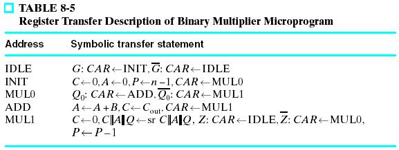
24 Control Signal Table (1/2) Control Signals for Binary Multiplier Bloc k Dia g ram Mod u l e Mi cr oo pe ra ti on Contr o l Si gn al N a me Contr o l Exp r e ssi on Register A : A 0 I nitia liz e IDLE G A A + B Load MUL0 Q 0 C A Q sr C A Q Shift_dec M UL1 Register B : B IN Load_B LO ADB F lip-f lop C : C 0 C lea r _C IDLE G + MUL1 C C ou t Load Register Q : Q IN Load_Q LO ADQ C A Q sr C A Q Shift_dec Cou n ter P : P n 1 I nitia liz e P P 1 Shift_dec 24
25 Control Signal Table (2/2) Signals are defined on a register basis. LOADQ and LOADB are external signals controlled from the system using the multiplier and will not be considered a part of this design. Note that many of the control signals are reused for different registers. These control signals are the outputs of the control unit. 25
26 Sequencing Part of ASM Next-state behavior State diagram remove -ops, conditional output boxes, & any decision box not affecting the next state IDLE 00 0 G 1 MUL0 01 MUL Z 1 26
27 Hardwired Control Control Design Methods The procedure from Chapter 6 Not suitable for a large amount of input states Procedure specializations that use a single signal to represent each state Sequence Register and Decoder Sequence register with encoded states, e.g., 00, 01, 10, 11. Decoder outputs produce state signals, e.g., 0001, 0010, 0100, One Flip-flop per State Flip-flop outputs as state signals, e. g., 0001, 0010, 0100,
28 Sequence Reg and Decoder Design (1/6) Initially, use sequential circuit design techniques from Chapter 6. First, define: States: IDLE, MUL0, MUL1 Input Signals: G, Z, Q 0 (Q 0 affects outputs, not next state) Output Signals: Initialize, LOAD, Shift_Dec, Clear_C State Transition Diagram (Use sequencing ASM) Output Function Second, find State Assignments (two bits required) We will use two state bits to encode the three state IDLE, MUL0, and MUL1. State M1 M0 IDLE 0 0 MUL0 0 1 MUL1 1 0 Unused
29 Sequence Reg and Decoder Design (2/6) Assuming that state variables M1 and M0 are decoded into states, the next state part of the state table is: Current State Input G Z Next State M1 M0 IDLE IDLE IDLE IDLE MUL MUL MUL MUL Current State M1 M0 Input G Z Next State M1 M0 MUL MUL MUL MUL Unused 0 0 d d Unused 0 1 d d Unused 1 0 d d Unused 1 1 d d 29
30 Sequence Reg and Decoder Design (3/6) 30
31 Sequence Reg and Decoder Design (5/6) Finding the state equations for M1 and M0 is easier due to the decoded states: D M1 = MUL0 D M0 = IDLE G + MUL1 Z Note that since there are five variables, a K-map is harder to use, so we have directly written reduced equations. The output equations using the decoded states: Initialize = IDLE G Load = MUL0 Q 0 Clear_C = IDLE G + MUL1 Shift_dec = MUL1 31
32 Sequence Reg and Decoder Design (5/6) Doing multiple level optimization, extract IDLE G: Initialize = IDLE G D M1 = MUL0 D M0 = Initialize + MUL1 Z Load = MUL0 Q 0 Clear_C = Initialize + MUL1 Shift_dec = MUL1 The resulting circuit using flip-flops, a decoder, and the above equations is given on the next slide. 32
33 Sequence Reg and Decoder Design (6/6) G Initalize D M 0 Initialize Clear_C Z C DECODER A0 A IDLE MUL0 MUL1 Shift_dec M 1 D C Q 0 Load Two one-bit seq regs + One 2-to-4 line decoder 33
34 One Flip-Flop per State This method uses one flip-flop per state and a simple set of transformation rules to implement the circuit. The design starts with the ASM chart, and replaces 1. State boxes with flip-flops, 2. Scalar decision boxes with a demultiplexer with 2 outputs, 3. Vector decision boxes with a (partial) demultiplexer 4. Junctions with an OR gate 5. Conditional outputs with AND gates. 34
35 State Box Transformation Rules Each state box transforms to a D flip-flop Entry point is connected to the input. Exit point is connected to the Q output. Entry STATE Entry STATE D Q Exit Exit 35
36 Scalar Decision Box Transformation Rules Each decision box transforms to a demultiplexer Entry point is an enable" input. The condition is the select" input. Decoded outputs are the exit points. Entry Entry X 0 X 1 Exit 0 Exit 1 Exit 0 Exit 1 36
37 Vector Decision Box Transformation Rules Each Decision box transforms to a demultiplexer Entry point is an enable input. The conditions are the select inputs. Demultiplexer outputs are the exit points. (Binary Vector Values) (Vector of Input Conditions) (Binary Vector Values) 10 X 1 11 X 1, X X 0 0 Entry DEMUX EN D 0 Exit 0 A 1 D 1 Exit 1 A 0 Exit2 D 2 D 3 Exit 3 37
38 Junction Transformation Rules Where two or more entry points join, connect the entry variables to an OR gate The exit is the output of the OR gate. Entry 1 Entry 2 Entry 1 Entry 2 Exit Exit 38
39 Conditional Output Box Rules Entry point is an enable input. The control OUTPUT is the same signal as the exit value. Entry Enable Entry X 1 X OUTPUT Exit 1 Exit 1 OUTPUT 39
40 Multiplier Example: Flip-flop per State Design Logic Diagram D 1 D 0 40
41 Microprogrammed Control Microprogrammed control: a control unit with its binary control values stored as words in memory (control memory) Microinstruction: -instr each word in the control memory, specifies one or more - ops for the system Microprogram: -prog a sequence of -instrs Microprogramming: places some representation for combinations of values of control variables in words of ROM for use by the rest of the control logic via successive read ops. 41
42 Microprogrammed Control Unit Organization The general configuration of a -p control: CM: control memory CAR: control addr reg CDR: control data reg (optional) Next-addr generator 42
43 Microprogrammed Control for Binary Multiplier ASM charts for -p controls: the seq ckts must be Moore-type no conditional output box is permitted in the ASM chart 43
44 Design of a -p Control Unit Determine the bits in the control word for the - instrs. -instr control word format Determine the sizes of the ROM (CM) and the CAR. Determine the structure of the next-addr generator and design the sequence Write the -prog. 44
45 -instr Control Word Format -instr control word format: Control signals to datapath Control outputs Next-address information (Sequencing) 45
46 Next-Address Information Two typical approaches to define the addrs: Method 1: two-addr-per- instr method Include the two addrs in the -instr controlling the decision. Based on the value of the decision variable, one of the two addr values is loaded into the CAR. CAR: a reg w/ parallel load Adv.: permits the arbitrary assignment of addrs to states (no states need to be added for the desired sequencing) Disadv.: requires 2 addrs in each -instr (wide ROM) Method 2: parallel-load counter method Use a counter with parallel load as the CAR. One of the two addrs is obtained from the -instr, but the other is obtained by counting up the CAR. Adv.: requires at most 1 addr per -instr Disadv.: states may have to be added for the desired sequencing (slower system) 46
47 Control Word Format Example (1/3) -instr control word format of the binary multiplier: Control signals: DATAPATH Control outputs: none Sequencing: 2 addr fields NXTADD1 NXTADD0 SEL 47
48 Control Word Format Example (2/3) Control signals: DATAPATH 48
49 Control Word Format Example (3/3) 49

50 Sizes of the ROM and the CAR 50
51 Structure of the Next-Addr Generator CAR NXTADD1 NXTADD0 SEL 51
52 Structure of the Microprogrammed Control Unit 52
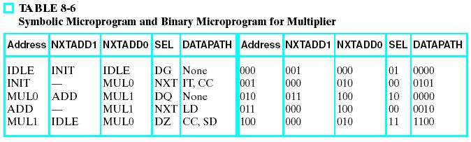
53 Microprogram 53
54 Summary Interaction b/t datapaths and control units Programmed vs. Nonprogrammed systems Algorithmic state machine (ASM): a means for representing and specifying control functions Example: Binary multiplier Hardwired control Basic design procedure Sequence reg plus decoder One flip-flop per state Microprogrammed control 54
Register Transfer Level in Verilog: Part II
 Source: M. Morris Mano and Michael D. Ciletti, Digital Design, 4rd Edition, 2007, Prentice Hall. Register Transfer Level in Verilog: Part II Lan-Da Van ( 范倫達 ), Ph. D. Department of Computer Science National
Registers and Counters
 Registers and Counters ( 范倫達 ), Ph. D. Department of Computer Science National Chiao Tung University Taiwan, R.O.C. Fall, 2011 ldvan@cs.nctu.edu.tw http://www.cs.nctu.edu.tw/~ldvan/ Registers Shift Registers
Registers and Counters
 Registers and Counters ( 范倫達 ), Ph. D. Department of Computer Science National Chiao Tung University Taiwan, R.O.C. Fall, 2017 ldvan@cs.nctu.edu.tw http://www.cs.nctu.edu.tw/~ldvan/ Registers Shift Registers
Modeling Digital Systems with Verilog
 Modeling Digital Systems with Verilog Prof. Chien-Nan Liu TEL: 03-4227151 ext:34534 Email: jimmy@ee.ncu.edu.tw 6-1 Composition of Digital Systems Most digital systems can be partitioned into two types
Digital Logic Design ENEE x. Lecture 24
 Digital Logic Design ENEE 244-010x Lecture 24 Announcements Homework 9 due today Thursday Office Hours (12/10) from 2:30-4pm Course Evaluations at the end of class today. https://www.courseevalum.umd.edu/
Synchronous Sequential Logic
 Synchronous Sequential Logic ( 范倫達 ), Ph. D. Department of Computer Science National Chiao Tung University Taiwan, R.O.C. Fall, 2017 ldvan@cs.nctu.edu.tw http://www.cs.nctu.edu.tw/~ldvan/ Outlines Sequential
Synchronous Sequential Logic
 Synchronous Sequential Logic ( 范倫達 ), Ph. D. Department of Computer Science National Chiao Tung University Taiwan, R.O.C. Fall, 2012 ldvan@cs.nctu.edu.tw http://www.cs.nctu.edu.tw/~ldvan/ Outlines Sequential
CSE Latches and Flip-flops Dr. Izadi. NOR gate property: A B Z Cross coupled NOR gates: S M S R Q M
 CSE-4523 Latches and Flip-flops Dr. Izadi NOR gate property: A B Z A B Z Cross coupled NOR gates: S M S R M R S M R S R S R M S S M R R S ' Gate R Gate S R S G R S R (t+) S G R Flip_flops:. S-R flip-flop
Chapter 3 Unit Combinational
 EE 200: Digital Logic Circuit Design Dr Radwan E Abdel-Aal, COE Logic and Computer Design Fundamentals Chapter 3 Unit Combinational 5 Registers Logic and Design Counters Part Implementation Technology
Microprocessor Design
 Microprocessor Design Principles and Practices With VHDL Enoch O. Hwang Brooks / Cole 2004 To my wife and children Windy, Jonathan and Michelle Contents 1. Designing a Microprocessor... 2 1.1 Overview
Advanced Devices. Registers Counters Multiplexers Decoders Adders. CSC258 Lecture Slides Steve Engels, 2006 Slide 1 of 20
 Advanced Devices Using a combination of gates and flip-flops, we can construct more sophisticated logical devices. These devices, while more complex, are still considered fundamental to basic logic design.
Chapter 5 Sequential Circuits
 Logic and Computer Design Fundamentals Chapter 5 Sequential Circuits Part 2 Sequential Circuit Design Charles Kime & Thomas Kaminski 28 Pearson Education, Inc. (Hyperlinks are active in View Show mode)
Logic and Computer Design Fundamentals. Chapter 7. Registers and Counters
 Logic and Computer Design Fundamentals Chapter 7 Registers and Counters Registers Register a collection of binary storage elements In theory, a register is sequential logic which can be defined by a state
ELEN Electronique numérique
 ELEN0040 - Electronique numérique Patricia ROUSSEAUX Année académique 2014-2015 CHAPITRE 6 Registers and Counters ELEN0040 6-277 Design of a modulo-8 binary counter using JK Flip-flops 3 bits are required
Objectives. Combinational logics Sequential logics Finite state machine Arithmetic circuits Datapath
 Objectives Combinational logics Sequential logics Finite state machine Arithmetic circuits Datapath In the previous chapters we have studied how to develop a specification from a given application, and
ELCT 501: Digital System Design
 ELCT 5: Digital System Lecture 8: System Dr. Mohamed Abd El Ghany, Algorithmic State Machine (ASM) For large machines, the designers often use a different form of representation, called the algorithmic
Fall 2000 Chapter 5 Part 1
 ECE/CS 352 Digital Systems Fundamentals Fall 2000 Chapter 5 Part 1 Tom Kaminski & Charles R. Kime ECE/CS 352 Digital System Fundamentals T. Kaminski & C. Kime 1 Registers A register is a collection of
Sequencing. Lan-Da Van ( 范倫達 ), Ph. D. Department of Computer Science National Chiao Tung University Taiwan, R.O.C. Fall,
, Ph. D. Department of Computer Science National Chiao Tung University Taiwan, R.O.C. Fall,") Sequencing ( 范倫達 ), Ph. D. Department of Computer Science National Chiao Tung University Taiwan, R.O.C. Fall, 2013 ldvan@cs.nctu.edu.tw http://www.cs.nctu.edu.tw/~ldvan/ Outlines Introduction Sequencing
Sequencing ( 范倫達 ), Ph. D. Department of Computer Science National Chiao Tung University Taiwan, R.O.C. Fall, 2013 ldvan@cs.nctu.edu.tw http://www.cs.nctu.edu.tw/~ldvan/ Outlines Introduction Sequencing
Administrative issues. Sequential logic
 Administrative issues Midterm #1 will be given Tuesday, October 29, at 9:30am. The entire class period (75 minutes) will be used. Open book, open notes. DDPP sections: 2.1 2.6, 2.10 2.13, 3.1 3.4, 3.7,
Control Unit. Arturo Díaz-Pérez Departamento de Computación Laboratorio de Tecnologías de Información CINVESTAV-IPN
 Control Unit Arturo Díaz-Pérez Departamento de Computación Laboratorio de Tecnologías de Información CINVESTAV-IPN Large Digital Systems In both combinational and sequential circuit design: small circuits
Chapter 6. Flip-Flops and Simple Flip-Flop Applications
 Chapter 6 Flip-Flops and Simple Flip-Flop Applications Basic bistable element It is a circuit having two stable conditions (states). It can be used to store binary symbols. J. C. Huang, 2004 Digital Logic
Contents Slide Set 6. Introduction to Chapter 7 of the textbook. Outline of Slide Set 6. An outline of the first part of Chapter 7
 CM 69 W4 Section Slide Set 6 slide 2/9 Contents Slide Set 6 for CM 69 Winter 24 Lecture Section Steve Norman, PhD, PEng Electrical & Computer Engineering Schulich School of Engineering University of Calgary
CS6201 UNIT I PART-A. Develop or build the following Boolean function with NAND gate F(x,y,z)=(1,2,3,5,7).
=(1,2,3,5,7).") VALLIAMMAI ENGINEERING COLLEGE SRM Nagar, Kattankulathur-603203 DEPARTMENT OF COMPUTER SCIENCE AND ENGINEERING Academic Year: 2015-16 BANK - EVEN SEMESTER UNIT I PART-A 1 Find the octal equivalent of hexadecimal
VALLIAMMAI ENGINEERING COLLEGE SRM Nagar, Kattankulathur-603203 DEPARTMENT OF COMPUTER SCIENCE AND ENGINEERING Academic Year: 2015-16 BANK - EVEN SEMESTER UNIT I PART-A 1 Find the octal equivalent of hexadecimal
Chapter 7 Registers and Register Transfers
 Logic and Computer Design Fundamentals Chapter 7 Registers and Register Transfers Part 3 Control of Register Transfers Charles Kime 2008 Pearson Education, Inc. (Hyperlinks are active in View Show mode)
Read-only memory (ROM) Digital logic: ALUs Sequential logic circuits. Don't cares. Bus
 Digital logic: ALUs Sequential logic circuits. Don't cares. Bus") Digital logic: ALUs Sequential logic circuits CS207, Fall 2004 October 11, 13, and 15, 2004 1 Read-only memory (ROM) A form of memory Contents fixed when circuit is created n input lines for 2 n addressable
Digital logic: ALUs Sequential logic circuits CS207, Fall 2004 October 11, 13, and 15, 2004 1 Read-only memory (ROM) A form of memory Contents fixed when circuit is created n input lines for 2 n addressable
CHAPTER1: Digital Logic Circuits
 CS224: Computer Organization S.KHABET CHAPTER1: Digital Logic Circuits 1 Sequential Circuits Introduction Composed of a combinational circuit to which the memory elements are connected to form a feedback
Registers & Counters. Logic and Digital System Design - CS 303 Erkay Savaş Sabanci University
 Registers & ounters Logic and igital System esign - S 33 Erkay Savaş Sabanci University Registers Registers like counters are clocked sequential circuits A register is a group of flip-flops Each flip-flop
The reduction in the number of flip-flops in a sequential circuit is referred to as the state-reduction problem.
 State Reduction The reduction in the number of flip-flops in a sequential circuit is referred to as the state-reduction problem. State-reduction algorithms are concerned with procedures for reducing the
Final Exam review: chapter 4 and 5. Supplement 3 and 4
 Final Exam review: chapter 4 and 5. Supplement 3 and 4 1. A new type of synchronous flip-flop has the following characteristic table. Find the corresponding excitation table with don t cares used as much
1. a) For the circuit shown in figure 1.1, draw a truth table showing the output Q for all combinations of inputs A, B and C. [4] Figure 1.
![1. a) For the circuit shown in figure 1.1, draw a truth table showing the output Q for all combinations of inputs A, B and C. [4] Figure 1.](/thumbs/88/117492374.jpg "1. a) For the circuit shown in figure 1.1, draw a truth table showing the output Q for all combinations of inputs A, B and C. [4] Figure 1.") [Question 1 is compulsory] 1. a) For the circuit shown in figure 1.1, draw a truth table showing the output Q for all combinations of inputs A, B and C. Figure 1.1 b) Minimize the following Boolean functions:
[Question 1 is compulsory] 1. a) For the circuit shown in figure 1.1, draw a truth table showing the output Q for all combinations of inputs A, B and C. Figure 1.1 b) Minimize the following Boolean functions:
We are here. Assembly Language. Processors Arithmetic Logic Units. Finite State Machines. Circuits Gates. Transistors
 CSC258 Week 5 1 We are here Assembly Language Processors Arithmetic Logic Units Devices Finite State Machines Flip-flops Circuits Gates Transistors 2 Circuits using flip-flops Now that we know about flip-flops
1. Convert the decimal number to binary, octal, and hexadecimal.
 1. Convert the decimal number 435.64 to binary, octal, and hexadecimal. 2. Part A. Convert the circuit below into NAND gates. Insert or remove inverters as necessary. Part B. What is the propagation delay
Lecture 12. Amirali Baniasadi
 CENG 24 Digital Design Lecture 2 Amirali Baniasadi amirali@ece.uvic.ca This Lecture Chapter 6: Registers and Counters 2 Registers Sequential circuits are classified based in their function, e.g., registers.
ELE2120 Digital Circuits and Systems. Tutorial Note 8
 ELE2120 Digital Circuits and Systems Tutorial Note 8 Outline 1. Register 2. Counters 3. Synchronous Counter 4. Asynchronous Counter 5. Sequential Circuit Design Overview 1. Register Applications: temporally
Page 1) 7 points Page 2) 16 points Page 3) 22 points Page 4) 21 points Page 5) 22 points Page 6) 12 points. TOTAL out of 100
 7 points Page 2) 16 points Page 3) 22 points Page 4) 21 points Page 5) 22 points Page 6) 12 points. TOTAL out of 100") EE3701 Dr. Gugel Spring 2014 Exam II ast Name First Open book/open notes, 90-minutes. Calculators are permitted. Write on the top of each page only. Page 1) 7 points Page 2) 16 points Page 3) 22 points
EE3701 Dr. Gugel Spring 2014 Exam II ast Name First Open book/open notes, 90-minutes. Calculators are permitted. Write on the top of each page only. Page 1) 7 points Page 2) 16 points Page 3) 22 points
DIGITAL SYSTEM DESIGN UNIT I (2 MARKS)
") DIGITAL SYSTEM DESIGN UNIT I (2 MARKS) 1. Convert Binary number (111101100) 2 to Octal equivalent. 2. Convert Binary (1101100010011011) 2 to Hexadecimal equivalent. 3. Simplify the following Boolean function
DIGITAL SYSTEM DESIGN UNIT I (2 MARKS) 1. Convert Binary number (111101100) 2 to Octal equivalent. 2. Convert Binary (1101100010011011) 2 to Hexadecimal equivalent. 3. Simplify the following Boolean function
 UNIT 1 NUMBER SYSTEMS AND DIGITAL LOGIC FAMILIES 1. Briefly explain the stream lined method of converting binary to decimal number with example. 2. Give the Gray code for the binary number (111) 2. 3.
ENGG 1203 Tutorial. D Flip Flop. D Flip Flop. Q changes when CLK is in Rising edge PGT NGT
 ENGG 1203 Tutorial D Flip Flop Sequential Logic 14/21 Feb Learning Objectives Design circuits with Flip Flop Design a finite state machine News Feb 27, 2014, 11:55pm Ack.: HKU ELEC1008, ISU CprE 281x,
Digital Logic Design I
 Digital Logic Design I Synchronous Sequential Logic Mustafa Kemal Uyguroğlu Sequential Circuits Asynchronous Inputs Combinational Circuit Memory Elements Outputs Synchronous Inputs Combinational Circuit
MODULE 3. Combinational & Sequential logic
 MODULE 3 Combinational & Sequential logic Combinational Logic Introduction Logic circuit may be classified into two categories. Combinational logic circuits 2. Sequential logic circuits A combinational
Chapter Contents. Appendix A: Digital Logic. Some Definitions
 A- Appendix A - Digital Logic A-2 Appendix A - Digital Logic Chapter Contents Principles of Computer Architecture Miles Murdocca and Vincent Heuring Appendix A: Digital Logic A. Introduction A.2 Combinational
MC9211 Computer Organization
 MC9211 Computer Organization Unit 2 : Combinational and Sequential Circuits Lesson2 : Sequential Circuits (KSB) (MCA) (2009-12/ODD) (2009-10/1 A&B) Coverage Lesson2 Outlines the formal procedures for the
Asynchronous (Ripple) Counters
 Counters") Circuits for counting events are frequently used in computers and other digital systems. Since a counter circuit must remember its past states, it has to possess memory. The chapter about flip-flops introduced
Circuits for counting events are frequently used in computers and other digital systems. Since a counter circuit must remember its past states, it has to possess memory. The chapter about flip-flops introduced
Chapter 3. Boolean Algebra and Digital Logic
 Chapter 3 Boolean Algebra and Digital Logic Chapter 3 Objectives Understand the relationship between Boolean logic and digital computer circuits. Learn how to design simple logic circuits. Understand how
Registers, Register Transfers and Counters Dr. Fethullah Karabiber
 36 OMPUTER HARWARE Registers, Register Transfers and ounters r. Fethullah Karabiber Overview 2 Registers, Microoperations and Implementations Registers and load enable Register transfer operations Microoperations
Sequential Logic Circuits
 Sequential Logic Circuits By Dr. M. Hebaishy Digital Logic Design Ch- Rem.!) Types of Logic Circuits Combinational Logic Memoryless Outputs determined by current values of inputs Sequential Logic Has memory
Principles of Computer Architecture. Appendix A: Digital Logic
 A-1 Appendix A - Digital Logic Principles of Computer Architecture Miles Murdocca and Vincent Heuring Appendix A: Digital Logic A-2 Appendix A - Digital Logic Chapter Contents A.1 Introduction A.2 Combinational
COE328 Course Outline. Fall 2007
 COE28 Course Outline Fall 2007 1 Objectives This course covers the basics of digital logic circuits and design. Through the basic understanding of Boolean algebra and number systems it introduces the student
Design Example: Demo Display Unit
 Design Example: Demo Display Unit Say we are given an arrangement of 8 LEDs in a diamond pattern, with the LED labelled 7 at the top of the diamond, then numbered down to 0 in the clockwise direction.
Tribhuvan University Institute of Science and Technology Bachelor of Science in Computer Science and Information Technology
 Tribhuvan University Institute of Science and Technology Bachelor of Science in Computer Science and Information Technology Course Title: Digital Logic Full Marks: 60 + 0 + 0 Course No.: CSC Pass Marks:
UNIVERSITI TEKNOLOGI MALAYSIA
 SULIT Faculty of Computing UNIVERSITI TEKNOLOGI MALAYSIA FINAL EXAMINATION SEMESTER I, 2016 / 2017 SUBJECT CODE : SUBJECT NAME : SECTION : TIME : DATE/DAY : VENUES : INSTRUCTIONS : Answer all questions
Introduction. Serial In - Serial Out Shift Registers (SISO)
") Introduction Shift registers are a type of sequential logic circuit, mainly for storage of digital data. They are a group of flip-flops connected in a chain so that the output from one flip-flop becomes
Introduction Shift registers are a type of sequential logic circuit, mainly for storage of digital data. They are a group of flip-flops connected in a chain so that the output from one flip-flop becomes
CprE 281: Digital Logic
 CprE 28: Digital Logic Instructor: Alexander Stoytchev http://www.ece.iastate.edu/~alexs/classes/ Registers and Counters CprE 28: Digital Logic Iowa State University, Ames, IA Copyright Alexander Stoytchev
AM AM AM AM PM PM PM
 FACULTY OF ENGINEERING AND TECHNOLOGY DEPARTMENT OF COMPUTER SCIENCE & ENGINEERING COURSE PLAN Course Code : CS0003 Course Title : DIGITAL COMPUTER FUNDAMENTALS Semester : III Course Time : Jun 204 to
Registers and Counters
 Registers and Counters Clocked sequential circuit = F/Fs and combinational gates Register Group of flip-flops (share a common clock and capable of storing one bit of information) Consist of a group of
Registers and Counters
 Registers and Counters A register is a group of flip-flops which share a common clock An n-bit register consists of a group of n flip-flops capable of storing n bits of binary information May have combinational
MODU LE DAY. Class-A, B, AB and C amplifiers - basic concepts, power, efficiency Basic concepts of Feedback and Oscillation. Day 1
 DAY MODU LE TOPIC QUESTIONS Day 1 Day 2 Day 3 Day 4 I Class-A, B, AB and C amplifiers - basic concepts, power, efficiency Basic concepts of Feedback and Oscillation Phase Shift Wein Bridge oscillators.
Bachelor Level/ First Year/ Second Semester/ Science Full Marks: 60 Computer Science and Information Technology (CSc. 151) Pass Marks: 24
 Pass Marks: 24") 2065 Computer Science and Information Technology (CSc. 151) Pass Marks: 24 Time: 3 hours. Candidates are required to give their answers in their own words as for as practicable. Attempt any TWO questions:
2065 Computer Science and Information Technology (CSc. 151) Pass Marks: 24 Time: 3 hours. Candidates are required to give their answers in their own words as for as practicable. Attempt any TWO questions:
DIGITAL ELECTRONICS MCQs
 DIGITAL ELECTRONICS MCQs 1. A 8-bit serial in / parallel out shift register contains the value 8, clock signal(s) will be required to shift the value completely out of the register. A. 1 B. 2 C. 4 D. 8
Combinational / Sequential Logic
 Digital Circuit Design and Language Combinational / Sequential Logic Chang, Ik Joon Kyunghee University Combinational Logic + The outputs are determined by the present inputs + Consist of input/output
CHAPTER 4 RESULTS & DISCUSSION
 CHAPTER 4 RESULTS & DISCUSSION 3.2 Introduction This project aims to prove that Modified Baugh-Wooley Two s Complement Signed Multiplier is one of the high speed multipliers. The schematic of the multiplier
Registers. Unit 12 Registers and Counters. Registers (D Flip-Flop based) Register Transfers (example not out of text) Accumulator Registers
 Register Transfers (example not out of text) Accumulator Registers") Unit 2 Registers and Counters Fundamentals of Logic esign EE2369 Prof. Eric Maconald Fall Semester 23 Registers Groups of flip-flops Can contain data format can be unsigned, 2 s complement and other more
Unit 2 Registers and Counters Fundamentals of Logic esign EE2369 Prof. Eric Maconald Fall Semester 23 Registers Groups of flip-flops Can contain data format can be unsigned, 2 s complement and other more
Solution to Digital Logic )What is the magnitude comparator? Design a logic circuit for 4 bit magnitude comparator and explain it,
What is the magnitude comparator? Design a logic circuit for 4 bit magnitude comparator and explain it,") Solution to Digital Logic -2067 Solution to digital logic 2067 1.)What is the magnitude comparator? Design a logic circuit for 4 bit magnitude comparator and explain it, A Magnitude comparator is a combinational
Solution to Digital Logic -2067 Solution to digital logic 2067 1.)What is the magnitude comparator? Design a logic circuit for 4 bit magnitude comparator and explain it, A Magnitude comparator is a combinational
Logic Design II (17.342) Spring Lecture Outline
 Spring Lecture Outline") Logic Design II (17.342) Spring 2012 Lecture Outline Class # 03 February 09, 2012 Dohn Bowden 1 Today s Lecture Registers and Counters Chapter 12 2 Course Admin 3 Administrative Admin for tonight Syllabus
Logic Design II (17.342) Spring 2012 Lecture Outline Class # 03 February 09, 2012 Dohn Bowden 1 Today s Lecture Registers and Counters Chapter 12 2 Course Admin 3 Administrative Admin for tonight Syllabus
Lecture 11: Synchronous Sequential Logic
 Lecture 11: Synchronous Sequential Logic Syed M. Mahmud, Ph.D ECE Department Wayne State University Aby K George, ECE Department, Wayne State University Contents Characteristic equations Analysis of clocked
Slide Set 6. for ENCM 369 Winter 2018 Section 01. Steve Norman, PhD, PEng
 Slide Set 6 for ENCM 369 Winter 2018 Section 01 Steve Norman, PhD, PEng Electrical & Computer Engineering Schulich School of Engineering University of Calgary February 2018 ENCM 369 Winter 2018 Section
DIGITAL ELECTRONICS & it0203 Semester 3
 DIGITAL ELECTRONICS & it0203 Semester 3 P.Rajasekar & C.M.T.Karthigeyan Asst.Professor SRM University, Kattankulathur School of Computing, Department of IT 8/22/20 Disclaimer The contents of the slides
Combinational vs Sequential
 Combinational vs Sequential inputs X Combinational Circuits outputs Z A combinational circuit: At any time, outputs depends only on inputs Changing inputs changes outputs No regard for previous inputs
Counters
 Counters A counter is the most versatile and useful subsystems in the digital system. A counter driven by a clock can be used to count the number of clock cycles. Since clock pulses occur at known intervals,
problem maximum score 1 28pts 2 10pts 3 10pts 4 15pts 5 14pts 6 12pts 7 11pts total 100pts
 University of California at Berkeley College of Engineering Department of Electrical Engineering and Computer Sciences EECS150 J. Wawrzynek Spring 2002 4/5/02 Midterm Exam II Name: Solutions ID number:
MAHARASHTRA STATE BOARD OF TECHNICAL EDUCATION (Autonomous) (ISO/IEC Certified)
 (ISO/IEC Certified)") Important Instructions to examiners: 1) The answers should be examined by key words and not as word-to-word as given in the model answer scheme. 2) The model answer and the answer written by candidate
Important Instructions to examiners: 1) The answers should be examined by key words and not as word-to-word as given in the model answer scheme. 2) The model answer and the answer written by candidate
Counter dan Register
 Counter dan Register Introduction Circuits for counting events are frequently used in computers and other digital systems. Since a counter circuit must remember its past states, it has to possess memory.
Computer Architecture and Organization
 A-1 Appendix A - Digital Logic Computer Architecture and Organization Miles Murdocca and Vincent Heuring Appendix A Digital Logic A-2 Appendix A - Digital Logic Chapter Contents A.1 Introduction A.2 Combinational
11.1 As mentioned in Experiment 10, sequential logic circuits are a type of logic circuit where the output
 EE 2449 Experiment JL and NWP //8 CALIFORNIA STATE UNIVERSITY LOS ANGELES Department of Electrical and Computer Engineering EE-2449 Digital Logic Lab EXPERIMENT SEQUENTIAL CIRCUITS Text: Mano and Ciletti,
Lab #12: 4-Bit Arithmetic Logic Unit (ALU)
") Lab #12: 4-Bit Arithmetic Logic Unit (ALU) ECE/COE 0501 Date of Experiment: 4/3/2017 Report Written: 4/5/2017 Submission Date: 4/10/2017 Nicholas Haver nicholas.haver@pitt.edu 1 H a v e r PURPOSE The purpose
Lab #12: 4-Bit Arithmetic Logic Unit (ALU) ECE/COE 0501 Date of Experiment: 4/3/2017 Report Written: 4/5/2017 Submission Date: 4/10/2017 Nicholas Haver nicholas.haver@pitt.edu 1 H a v e r PURPOSE The purpose
LESSON PLAN. Sub Code: EE2255 Sub Name: DIGITAL LOGIC CIRCUITS Unit: I Branch: EEE Semester: IV
 Unit: I Branch: EEE Semester: IV Page 1 of 6 Unit I Syllabus: BOOLEAN ALGEBRA AND COMBINATIONAL CIRCUITS 9 Boolean algebra: De-Morgan s theorem, switching functions and simplification using K-maps & Quine
Contents Circuits... 1
 Contents Circuits... 1 Categories of Circuits... 1 Description of the operations of circuits... 2 Classification of Combinational Logic... 2 1. Adder... 3 2. Decoder:... 3 Memory Address Decoder... 5 Encoder...
BCN1043. By Dr. Mritha Ramalingam. Faculty of Computer Systems & Software Engineering
 BCN1043 By Dr. Mritha Ramalingam Faculty of Computer Systems & Software Engineering mritha@ump.edu.my http://ocw.ump.edu.my/ authors Dr. Mohd Nizam Mohmad Kahar (mnizam@ump.edu.my) Jamaludin Sallim (jamal@ump.edu.my)
Logic Design II (17.342) Spring Lecture Outline
 Spring Lecture Outline") Logic Design II (17.342) Spring 2012 Lecture Outline Class # 05 February 23, 2012 Dohn Bowden 1 Today s Lecture Analysis of Clocked Sequential Circuits Chapter 13 2 Course Admin 3 Administrative Admin
Logic Design II (17.342) Spring 2012 Lecture Outline Class # 05 February 23, 2012 Dohn Bowden 1 Today s Lecture Analysis of Clocked Sequential Circuits Chapter 13 2 Course Admin 3 Administrative Admin
Figure 30.1a Timing diagram of the divide by 60 minutes/seconds counter
 Digital Clock The timing diagram figure 30.1a shows the time interval t 6 to t 11 and t 19 to t 21. At time interval t 9 the units counter counts to 1001 (9) which is the terminal count of the 74x160 decade
6.3 Sequential Circuits (plus a few Combinational)
") 6.3 Sequential Circuits (plus a few Combinational) Logic Gates: Fundamental Building Blocks Introduction to Computer Science Robert Sedgewick and Kevin Wayne Copyright 2005 http://www.cs.princeton.edu/introcs
6.3 Sequential Circuits (plus a few Combinational) Logic Gates: Fundamental Building Blocks Introduction to Computer Science Robert Sedgewick and Kevin Wayne Copyright 2005 http://www.cs.princeton.edu/introcs
Find the equivalent decimal value for the given value Other number system to decimal ( Sample)
") VELAMMAL COLLEGE OF ENGINEERING AND TECHNOLOGY, MADURAI 65 009 Department of Information Technology Model Exam-II-Question bank PART A (Answer for all Questions) (8 X = 6) K CO Marks Find the equivalent
VELAMMAL COLLEGE OF ENGINEERING AND TECHNOLOGY, MADURAI 65 009 Department of Information Technology Model Exam-II-Question bank PART A (Answer for all Questions) (8 X = 6) K CO Marks Find the equivalent
Good Evening! Welcome!
 Page 1/11 Instructions: urn off all cell phones, beepers and other noise making devices. Show all work on the front of the test papers. Box each answer. If you need more room, make a clearly indicated
Previous Lecture Sequential Circuits. Slide Summary of contents covered in this lecture. (Refer Slide Time: 01:55)
") Previous Lecture Sequential Circuits Digital VLSI System Design Prof. S. Srinivasan Department of Electrical Engineering Indian Institute of Technology, Madras Lecture No 7 Sequential Circuit Design Slide
Previous Lecture Sequential Circuits Digital VLSI System Design Prof. S. Srinivasan Department of Electrical Engineering Indian Institute of Technology, Madras Lecture No 7 Sequential Circuit Design Slide
Introduction to Digital Logic Missouri S&T University CPE 2210 Exam 3 Logistics
 Introduction to Digital Logic Missouri S&T University CPE 2210 Exam 3 Logistics Egemen K. Çetinkaya Egemen K. Çetinkaya Department of Electrical & Computer Engineering Missouri University of Science and
Logic Design Viva Question Bank Compiled By Channveer Patil
 Logic Design Viva Question Bank Compiled By Channveer Patil Title of the Practical: Verify the truth table of logic gates AND, OR, NOT, NAND and NOR gates/ Design Basic Gates Using NAND/NOR gates. Q.1
Chapter 4. Logic Design
 Chapter 4 Logic Design 4.1 Introduction. In previous Chapter we studied gates and combinational circuits, which made by gates (AND, OR, NOT etc.). That can be represented by circuit diagram, truth table
Flip-Flops and Sequential Circuit Design
 Flip-Flops and Sequential Circuit Design ECE 52 Summer 29 Reading ssignment Brown and Vranesic 7 Flip-Flops, Registers, Counters and a Simple Processor 7.5 T Flip-Flop 7.5. Configurable Flip-Flops 7.6
Using minterms, m-notation / decimal notation Sum = Cout = Using maxterms, M-notation Sum = Cout =
 1 Review of Digital Logic Design Fundamentals Logic circuits: 1. Combinational Logic: No memory, present output depends only on the present input 2. Sequential Logic: Has memory, present output depends
Computer Systems Architecture
 Computer Systems Architecture Fundamentals Of Digital Logic 1 Our Goal Understand Fundamentals and basics Concepts How computers work at the lowest level Avoid whenever possible Complexity Implementation
ROEVER COLLEGE OF ENGINEERING & TECHNOLOGY ELAMBALUR, PERAMBALUR DEPARTMENT OF ELECTRICAL AND ELECTRONICS ENGINEERING
 ROEVER COLLEGE OF ENGINEERING & TECHNOLOGY ELAMBALUR, PERAMBALUR-621220 DEPARTMENT OF ELECTRICAL AND ELECTRONICS ENGINEERING DIGITAL LOGIC CIRCUITS UNIT-1 BOOLEAN ALGEBRA AND COMBINATIONAL CIRCUITS 1.
CSE115: Digital Design Lecture 23: Latches & Flip-Flops
 Faculty of Engineering CSE115: Digital Design Lecture 23: Latches & Flip-Flops Sections 7.1-7.2 Suggested Reading A Generic Digital Processor Building Blocks for Digital Architectures INPUT - OUTPUT Interconnect:
Switching Circuits & Logic Design, Fall Final Examination (1/13/2012, 3:30pm~5:20pm)
") Switching Circuits & Logic Design, Fall 2011 Final Examination (1/13/2012, 3:30pm~5:20pm) Problem 1: (15 points) Consider a new FF with three inputs, S, R, and T. No more than one of these inputs can be
Switching Circuits & Logic Design, Fall 2011 Final Examination (1/13/2012, 3:30pm~5:20pm) Problem 1: (15 points) Consider a new FF with three inputs, S, R, and T. No more than one of these inputs can be
ECE 263 Digital Systems, Fall 2015
 ECE 263 Digital Systems, Fall 2015 REVIEW: FINALS MEMORY ROM, PROM, EPROM, EEPROM, FLASH RAM, DRAM, SRAM Design of a memory cell 1. Draw circuits and write 2 differences and 2 similarities between DRAM
Chapter 6 Registers and Counters
 EEA051 - Digital Logic 數位邏輯 Chapter 6 Registers and Counters 吳俊興國立高雄大學資訊工程學系 January 2006 Chapter 6 Registers and Counters 6-1 Registers 6-2 Shift Registers 6-3 Ripple Counters 6-4 Synchronous Counters
CSC Computer Architecture and Organization
 S 37 - omputer Architecture and Organization Lecture 6: Registers and ounters Registers A register is a group of flip-flops. Each flip-flop stores one bit of data; n flip-flops are required to store n
FPGA Implementation of Sequential Logic
 ECE 428 Programmable ASIC Design FPGA Implementation of Sequential Logic Haibo Wang ECE Department Southern Illinois University Carbondale, IL 62901 8-1 Sequential Circuit Model Combinational Circuit:
Chapter 5: Synchronous Sequential Logic
 Chapter 5: Synchronous Sequential Logic NCNU_2016_DD_5_1 Digital systems may contain memory for storing information. Combinational circuits contains no memory elements the outputs depends only on the inputs
Flip Flop. S-R Flip Flop. Sequential Circuits. Block diagram. Prepared by:- Anwar Bari
 Sequential Circuits The combinational circuit does not use any memory. Hence the previous state of input does not have any effect on the present state of the circuit. But sequential circuit has memory
Department of Electrical and Computer Engineering Mid-Term Examination Winter 2012
 1 McGill University Faculty of Engineering ECSE-221B Introduction to Computer Engineering Department of Electrical and Computer Engineering Mid-Term Examination Winter 2012 Examiner: Rola Harmouche Date: