CS/EE Homework 6
|
|
|
- Amy Osborne
- 5 years ago
- Views:
Transcription
1 CS/EE Homework 6 Due 3/16/ Use VHDL to design the 4 bit arithmetic unit specified in problem 4 of homework 5 (you may borrow from the posted solution, if you wish). Use a dataflow description to define basic building blocks for each component (e.g. half-adders and full-adders), then use structural VHDL to assemble these into larger components, and to assemble the components into the complete circuit. Simulate the circuit on the same inputs as in homework 5. entity flip is en: in STD_LOGIC; a: in STD_LOGIC_VECTOR (3 downto 0 x: out STD_LOGIC_VECTOR (3 downto 0) end flip; architecture flip_arch of flip is x <= (not a) when en = '1' else a; end flip_arch; entity inc is en: in STD_LOGIC; a: in STD_LOGIC_VECTOR (3 downto 0 x: out STD_LOGIC_VECTOR (3 downto 0) end inc; architecture inc_arch of inc is signal c: STD_LOGIC_VECTOR (2 downto 0 c(0) <= a(0) and en; c(1) <= a(1) and c(0 c(2) <= a(2) and c(1 x(0) <= a(0) xor en; x(1) <= a(1) xor c(0 x(2) <= a(2) xor c(1-1 -
2 x(3) <= a(3) xor c(2 end inc_arch; entity pass is en: in STD_LOGIC; a: in STD_LOGIC_VECTOR (3 downto 0 x: out STD_LOGIC_VECTOR (3 downto 0) end pass; architecture pass_arch of pass is x <= a when en = '1' else "0000"; end pass_arch; entity adder is cin: in STD_LOGIC; a, b: in STD_LOGIC_VECTOR (3 downto 0 x: out STD_LOGIC_VECTOR (3 downto 0 cout: out STD_LOGIC end adder; architecture adder_arch of adder is signal c: STD_LOGIC_VECTOR (3 downto 0 c(0)<=(a(0) and b(0)) or (a(0) and cin) or (b(0) and cin c(1)<=(a(1) and b(1)) or (a(1) and c(0)) or (b(1) and c(0) c(2)<=(a(2) and b(2)) or (a(2) and c(1)) or (b(2) and c(1) c(3)<=(a(3) and b(3)) or (a(3) and c(2)) or (b(3) and c(2) cout <= c(3 x(0) <= a(0) xor (b(0) xor cin x(1) <= a(1) xor (b(1) xor c(0) x(2) <= a(2) xor (b(2) xor c(1) x(3) <= a(3) xor (b(3) xor c(2) end adder_arch; entity control is c: in STD_LOGIC_VECTOR (2 downto 0-2 -
3 sa, sb, sx, adder_cout: in STD_LOGIC; na, nb, pa, pb, v: out STD_LOGIC end control; architecture control_arch of control is na <= '1' when (c = "010") or (c = "111") else '0'; nb <= '1' when (c = "011") or (c = "110") else '0'; pa <= '1' when (c /= "001") and (c /= "011") else '0'; pb <= '1' when (c /= "000") and (c /= "010") else '0'; v <= '1' when ((c = "010") and sa = '1' and sx = '1') or ((c = "011") and sb = '1' and sx = '1') or ((c = "100") and adder_cout = '1') or ((c = "101") and (sa = sb) and (sa /= sx)) or ((c = "110") and (sa /= sb) and (sa /= sx)) or ((c = "111") and (sa /= sb) and (sb /= sx)) else '0'; end control_arch; entity arithuvs is a, b: in STD_LOGIC_VECTOR (3 downto 0 c: in STD_LOGIC_VECTOR (2 downto 0 x: out STD_LOGIC_VECTOR (3 downto 0 v: out STD_LOGIC end arithuvs; architecture arithuvs_arch of arithuvs is component flip en: in STD_LOGIC; a: in STD_LOGIC_VECTOR (3 downto 0 x: out STD_LOGIC_VECTOR (3 downto 0) end component; component inc en: in STD_LOGIC; a: in STD_LOGIC_VECTOR (3 downto 0 x: out STD_LOGIC_VECTOR (3 downto 0) end component; component pass en: in STD_LOGIC; a: in STD_LOGIC_VECTOR (3 downto 0 x: out STD_LOGIC_VECTOR (3 downto 0) end component; - 3 -
4 component adder cin: in STD_LOGIC; a, b: in STD_LOGIC_VECTOR (3 downto 0 x: out STD_LOGIC_VECTOR (3 downto 0 cout: out STD_LOGIC end component; component control c: in STD_LOGIC_VECTOR (2 downto 0 sa, sb, sx, adder_cout: in STD_LOGIC; na, nb, pa, pb, v: out STD_LOGIC end component; signal a1, a2, a3, b1, b2, b3, xb: STD_LOGIC_VECTOR (3 downto 0 signal na, nb, pa, pb, adder_cout: STD_LOGIC; signal zero: STD_LOGIC; zero <= '0'; flip_a: flip port map(na, a, a1 flip_b: flip port map(nb, b, b1 inc_a: inc port map(na, a1, a2 inc_b: inc port map(nb, b1, b2 pass_a: pass port map(pa, a2, a3 pass_b: pass port map(pb, b2, b3 addem: adder port map(zero,a3,b3,xb,adder_cout ctl: control port map(c,a(3),b(3),xb(3), adder_cout, na, nb, pa, pb, v x <= xb; end arithuvs_arch; - 4 -
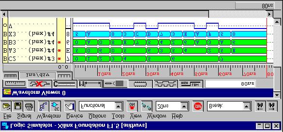
5 - 5 -
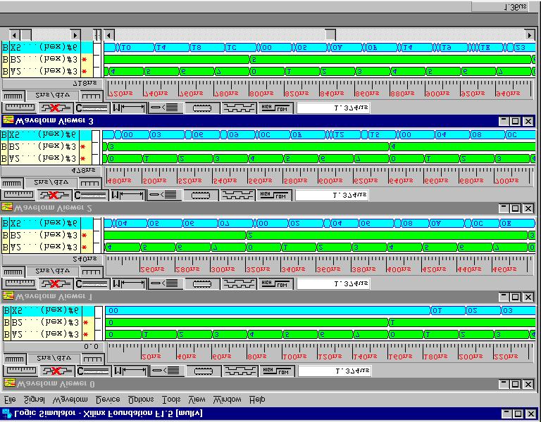
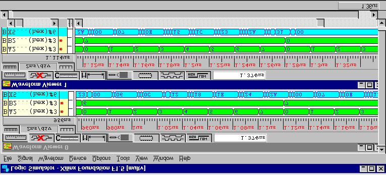
6 2. Write a VHDL specification for a 3 bit multiplier with 6 output bits. Your specification should include a 3 bit adder module. Use structural VHDL to combine the adder modules to form the multiplier. Perform a unit delay simulation of your circuit for all 64 possible pairs of input values and display the results so that inputs and outputs are represented numerically (that is, combine the signals to form a bus) so that the results are easy to check. In your simulation, set the simulation precision to 1 ns and have the inputs change once every 20 ns. entity adder is cin: in STD_LOGIC; a, b: in STD_LOGIC_VECTOR (2 downto 0 x: out STD_LOGIC_VECTOR (2 downto 0 cout: out STD_LOGIC end adder; architecture adder_arch of adder is signal c: STD_LOGIC_VECTOR (2 downto 0 c(0) <= (a(0) and b(0)) or (a(0) and cin) or (b(0) and cin c(1) <= (a(1) and b(1)) or (a(1) and c(0)) or (b(1) and c(0) c(2) <= (a(2) and b(2)) or (a(2) and c(1)) or (b(2) and c(1) cout <= c(2 x(0) <= a(0) xor (b(0) xor cin x(1) <= a(1) xor (b(1) xor c(0) x(2) <= a(2) xor (b(2) xor c(1) end adder_arch; entity mult is a, b: in STD_LOGIC_VECTOR (2 downto 0 x: out STD_LOGIC_VECTOR (5 downto 0) end mult; architecture mult_arch of mult is component adder cin: in STD_LOGIC; a, b: in STD_LOGIC_VECTOR (2 downto 0 x: out STD_LOGIC_VECTOR (2 downto 0 cout: out STD_LOGIC end component; signal pp0, pp1, pp2, spp0: STD_LOGIC_VECTOR (2 downto 0 signal isum: STD_LOGIC_VECTOR (3 downto 0 signal zero: STD_LOGIC; zero <= '0'; - 6 -
7 pp0 <= a when b(0) = '1' else "000"; pp1 <= a when b(1) = '1' else "000"; pp2 <= a when b(2) = '1' else "000"; spp0 <= '0' & pp0(2 downto 1 add0: adder port map(zero, pp1, spp0, isum(2 downto 0), isum(3) add1: adder port map(zero, pp2, isum(3 downto 1), x(4 downto 2), x(5) x(1) <= isum(0 x(0) <= pp0(0 end mult_arch; - 7 -
8 - 8 -
9 - 9 -
10 3. Consider the flip flop in Figure 4-35 of Mano & Kime. Construct (by hand) a timing diagram for this circuit to determine how it behaves. Show the C and D inputs, the intermediate S and R signals and the Q and Q outputs. To understand how the circuit works, consider the diagram shown below. A C.. S R... Q Q D. B The first thing to do is note that when C=0, the S and R signals are both high. This means that the output latch just retains its old value. So, whenever C=0, there is no change to Q and Q'. Also, when C=0, signal B equals D' (the complement of the D input). Because of this, signal A equals D. Now, consider what happens when C changes from 0 to 1,while D stays stable. The two inner NANDs on the left hand side are now enabled. So in particular, the second one from the top propagates the value on the other input to its output (complementing it, as it propagates).this makes the S signal equal to D'. Now, the second NAND from the bottom has C=1 at one input and has D' at both of its other inputs. So its output will be D. That is R will be D. So now the output latch has complementary values on its inputs and will propagate these to the outputs, so that we will have Q=D and Q'=D'. Now, the last thing to note is that after C goes high, subsequent changes to the D input don't affect the stored value, because after the transition, the feedback input of the bottom NAND is equal to D. If the D input now changes to D', this NAND will have different values on its two inputs, so signal B will be high. But this high output just reinforces the feedback through the top NAND gate, without allowing any other signal values to change. So all changes to D that follow the rising clock edge have no effect on the output value
11 So the circuit operates as a positive edge-triggered D flip flop. Note that it is important that the D input stays stable when the clock is rising. If this condition is not met, the operation of the circuit is unpredictable and can include oscillations on the outputs. C D S R Q Q
12 4. Derive a state transition diagram ( bubble diagram) for the sequential circuit shown below. Give a set of test inputs for this circuit that will verify every transition in the state diagram (including self-loops ). D R clk D >C Q Q Z 00/1 10/0 *1/ /1 DR/Z *1/0 00/0 The following sequence exercises all the transitions. D = R =
Feedback Sequential Circuits
 Feedback Sequential Circuits sequential circuit output depends on 1. current inputs 2. past sequence of inputs current state feedback sequential circuit uses ordinary gates and feedback loops to create
Flip-flop and Registers
 ECE 322 Digital Design with VHDL Flip-flop and Registers Lecture Textbook References n Sequential Logic Review Stephen Brown and Zvonko Vranesic, Fundamentals of Digital Logic with VHDL Design, 2 nd or
hochschule fu r angewandte wissenschaften hamburg Prof. Dr. B. Schwarz FB Elektrotechnik/Informatik
 8 Shift Registers A Johnson counter contains the basic structure of a shift register which is made up by a chain of D- FFs. Beginning with the LSB of a register (a number of D-FFs) each D-FF output can
ECE 263 Digital Systems, Fall 2015
 ECE 263 Digital Systems, Fall 2015 REVIEW: FINALS MEMORY ROM, PROM, EPROM, EEPROM, FLASH RAM, DRAM, SRAM Design of a memory cell 1. Draw circuits and write 2 differences and 2 similarities between DRAM
Synchronous Sequential Logic
 Synchronous Sequential Logic -A Sequential Circuit consists of a combinational circuit to which storage elements are connected to form a feedback path. The storage elements are devices capable of storing
HDL & High Level Synthesize (EEET 2035) Laboratory II Sequential Circuits with VHDL: DFF, Counter, TFF and Timer
 Laboratory II Sequential Circuits with VHDL: DFF, Counter, TFF and Timer") 1 P a g e HDL & High Level Synthesize (EEET 2035) Laboratory II Sequential Circuits with VHDL: DFF, Counter, TFF and Timer Objectives: Develop the behavioural style VHDL code for D-Flip Flop using gated,
1 P a g e HDL & High Level Synthesize (EEET 2035) Laboratory II Sequential Circuits with VHDL: DFF, Counter, TFF and Timer Objectives: Develop the behavioural style VHDL code for D-Flip Flop using gated,
Sequential Design Basics
 Sequential Design Basics Lecture 2 topics A review of devices that hold state A review of Latches A review of Flip-Flops Unit of text Set-Reset Latch/Flip-Flops/D latch/ Edge triggered D Flip-Flop 8/22/22
MASSACHUSETTS INSTITUTE OF TECHNOLOGY Department of Electrical Engineering and Computer Sciences
 MASSACHUSETTS INSTITUTE OF TECHNOLOGY Department of Electrical Engineering and Computer Sciences Introductory Digital Systems Lab (6.111) Quiz #2 - Spring 2003 Prof. Anantha Chandrakasan and Prof. Don
D Latch (Transparent Latch)
") D Latch (Transparent Latch) -One way to eliminate the undesirable condition of the indeterminate state in the SR latch is to ensure that inputs S and R are never equal to 1 at the same time. This is done
D Latch (Transparent Latch) -One way to eliminate the undesirable condition of the indeterminate state in the SR latch is to ensure that inputs S and R are never equal to 1 at the same time. This is done
Digital Fundamentals: A Systems Approach
 Digital Fundamentals: A Systems Approach Latches, Flip-Flops, and Timers Chapter 6 Traffic Signal Control Traffic Signal Control: State Diagram Traffic Signal Control: Block Diagram Traffic Signal Control:
CSE Latches and Flip-flops Dr. Izadi. NOR gate property: A B Z Cross coupled NOR gates: S M S R Q M
 CSE-4523 Latches and Flip-flops Dr. Izadi NOR gate property: A B Z A B Z Cross coupled NOR gates: S M S R M R S M R S R S R M S S M R R S ' Gate R Gate S R S G R S R (t+) S G R Flip_flops:. S-R flip-flop
ECE 341. Lecture # 2
 ECE 341 Lecture # 2 Instructor: Zeshan Chishti zeshan@pdx.edu October 1, 2014 Portland State University Announcements Course website reminder: http://www.ece.pdx.edu/~zeshan/ece341.htm Homework 1: Will
The outputs are formed by a combinational logic function of the inputs to the circuit or the values stored in the flip-flops (or both).
.") 1 The outputs are formed by a combinational logic function of the inputs to the circuit or the values stored in the flip-flops (or both). The value that is stored in a flip-flop when the clock pulse occurs
1 The outputs are formed by a combinational logic function of the inputs to the circuit or the values stored in the flip-flops (or both). The value that is stored in a flip-flop when the clock pulse occurs
CHAPTER 1 LATCHES & FLIP-FLOPS
 CHAPTER 1 LATCHES & FLIP-FLOPS 1 Outcome After learning this chapter, student should be able to; Recognize the difference between latches and flipflops Analyze the operation of the flip flop Draw the output
ELE2120 Digital Circuits and Systems. Tutorial Note 7
 ELE2120 Digital Circuits and Systems Tutorial Note 7 Outline 1. Sequential Circuit 2. Gated SR Latch 3. Gated D-latch 4. Edge-Triggered D Flip-Flop 5. Asynchronous and Synchronous reset Sequential Circuit
Lecture 8: Sequential Logic
 Lecture 8: Sequential Logic Last lecture discussed how we can use digital electronics to do combinatorial logic we designed circuits that gave an immediate output when presented with a given set of inputs
LAB #4 SEQUENTIAL LOGIC CIRCUIT
 LAB #4 SEQUENTIAL LOGIC CIRCUIT OBJECTIVES 1. To learn how basic sequential logic circuit works 2. To test and investigate the operation of various latch and flip flop circuits INTRODUCTIONS Sequential
(CSC-3501) Lecture 7 (07 Feb 2008) Seung-Jong Park (Jay) CSC S.J. Park. Announcement
 Lecture 7 (07 Feb 2008) Seung-Jong Park (Jay) CSC S.J. Park. Announcement") Seung-Jong Park (Jay) http://www.csc.lsu.edu/~sjpark Computer Architecture (CSC-3501) Lecture 7 (07 Feb 2008) 1 Announcement 2 1 Combinational vs. Sequential Logic Combinational Logic Memoryless Outputs
Seung-Jong Park (Jay) http://www.csc.lsu.edu/~sjpark Computer Architecture (CSC-3501) Lecture 7 (07 Feb 2008) 1 Announcement 2 1 Combinational vs. Sequential Logic Combinational Logic Memoryless Outputs
Logic Design. Flip Flops, Registers and Counters
 Logic Design Flip Flops, Registers and Counters Introduction Combinational circuits: value of each output depends only on the values of inputs Sequential Circuits: values of outputs depend on inputs and
EMT 125 Digital Electronic Principles I CHAPTER 6 : FLIP-FLOP
 EMT 125 Digital Electronic Principles I CHAPTER 6 : FLIP-FLOP 1 Chapter Overview Latches Gated Latches Edge-triggered flip-flops Master-slave flip-flops Flip-flop operating characteristics Flip-flop applications
Eng. Mohammed Samara. Fall The Islamic University of Gaza. Faculty of Engineering. Computer Engineering Department
 Fall 2011 The Islamic University of Gaza Faculty of Engineering Computer Engineering Department ECOM 4111 - Digital Systems Design Lab Lab 7: Prepared By: Eng. Mohammed Samara Introduction: A counter is
ACS College of Engineering. Department of Biomedical Engineering. HDL pre lab questions ( ) Cycle-1
 Cycle-1") ACS College of Engineering Department of Biomedical Engineering HDL pre lab questions (2015-2016) Cycle-1 1. What is truth table? 2. Which gates are called universal gates? 3. Define HDL? 4. What is the
ACS College of Engineering Department of Biomedical Engineering HDL pre lab questions (2015-2016) Cycle-1 1. What is truth table? 2. Which gates are called universal gates? 3. Define HDL? 4. What is the
MODULE 3. Combinational & Sequential logic
 MODULE 3 Combinational & Sequential logic Combinational Logic Introduction Logic circuit may be classified into two categories. Combinational logic circuits 2. Sequential logic circuits A combinational
Multiplexor (aka MUX) An example, yet VERY useful circuit!
 An example, yet VERY useful circuit!") Multiplexor (aka MUX) An example, yet VERY useful circuit! A B 0 1 Y S A B Y 0 0 x 0 0 1 x 1 1 x 0 0 1 x 1 1 S=1 S=0 Y = (S)? B:A; Y=S A+SB when S = 0: output A 1: output B 56 A 32-bit MUX Use 32 1-bit
Multiplexor (aka MUX) An example, yet VERY useful circuit! A B 0 1 Y S A B Y 0 0 x 0 0 1 x 1 1 x 0 0 1 x 1 1 S=1 S=0 Y = (S)? B:A; Y=S A+SB when S = 0: output A 1: output B 56 A 32-bit MUX Use 32 1-bit
Module 4:FLIP-FLOP. Quote of the day. Never think you are nothing, never think you are everything, but think you are something and achieve anything.
 Module 4:FLIP-FLOP Quote of the day Never think you are nothing, never think you are everything, but think you are something and achieve anything. Albert Einstein Sequential and combinational circuits
IS1500 (not part of IS1200) Logic Design Lab (LD-Lab)
 Logic Design Lab (LD-Lab)") Introduction IS1500 (not part of IS1200) Logic Design Lab (LD-Lab) 2017-10-26 The purpose of this lab is to give a hands-on experience of using gates and digital building blocks. These build blocks are
Introduction IS1500 (not part of IS1200) Logic Design Lab (LD-Lab) 2017-10-26 The purpose of this lab is to give a hands-on experience of using gates and digital building blocks. These build blocks are
Sequential logic circuits
 Computer Mathematics Week 10 Sequential logic circuits College of Information Science and Engineering Ritsumeikan University last week combinational digital circuits signals and busses logic gates and,
6.3 Sequential Circuits (plus a few Combinational)
") 6.3 Sequential Circuits (plus a few Combinational) Logic Gates: Fundamental Building Blocks Introduction to Computer Science Robert Sedgewick and Kevin Wayne Copyright 2005 http://www.cs.princeton.edu/introcs
6.3 Sequential Circuits (plus a few Combinational) Logic Gates: Fundamental Building Blocks Introduction to Computer Science Robert Sedgewick and Kevin Wayne Copyright 2005 http://www.cs.princeton.edu/introcs
Ryerson University Department of Electrical and Computer Engineering EES508 Digital Systems
 1 P a g e Ryerson University Department of Electrical and Computer Engineering EES508 Digital Systems Lab 5 - VHDL for Sequential Circuits: Implementing a customized State Machine 15 Marks ( 2 weeks) Due
COMP sequential logic 1 Jan. 25, 2016
 OMP 273 5 - sequential logic 1 Jan. 25, 2016 Sequential ircuits All of the circuits that I have discussed up to now are combinational digital circuits. For these circuits, each output is a logical combination
Chapter 1: Switching Algebra Chapter 2: Logical Levels, Timing & Delays. Introduction to latches Chapter 9: Binary Arithmetic
 12.12.216 Chapter 5 Flip Flops Dr.-ng. Stefan Werner /14 Table of content Chapter 1: Switching Algebra Chapter 2: Logical Levels, Timing & Delays Chapter 3: Karnaugh-Veitch-Maps Chapter 4: Combinational
CSE115: Digital Design Lecture 23: Latches & Flip-Flops
 Faculty of Engineering CSE115: Digital Design Lecture 23: Latches & Flip-Flops Sections 7.1-7.2 Suggested Reading A Generic Digital Processor Building Blocks for Digital Architectures INPUT - OUTPUT Interconnect:
YEDITEPE UNIVERSITY DEPARTMENT OF COMPUTER ENGINEERING. EXPERIMENT VIII: FLIP-FLOPS, COUNTERS 2014 Fall
 YEDITEPE UNIVERSITY DEPARTMENT OF COMPUTER ENGINEERING EXPERIMENT VIII: FLIP-FLOPS, COUNTERS 2014 Fall Objective: - Dealing with the operation of simple sequential devices. Learning invalid condition in
VeriLab. An introductory lab for using Verilog in digital design (first draft) VeriLab
 VeriLab") VeriLab An introductory lab for using Verilog in digital design (first draft) VeriLab An introductory lab for using Verilog in digital design Verilog is a hardware description language useful for designing
VeriLab An introductory lab for using Verilog in digital design (first draft) VeriLab An introductory lab for using Verilog in digital design Verilog is a hardware description language useful for designing
CHAPTER 4 RESULTS & DISCUSSION
 CHAPTER 4 RESULTS & DISCUSSION 3.2 Introduction This project aims to prove that Modified Baugh-Wooley Two s Complement Signed Multiplier is one of the high speed multipliers. The schematic of the multiplier
Sequential Logic Circuits
 Sequential Logic Circuits By Dr. M. Hebaishy Digital Logic Design Ch- Rem.!) Types of Logic Circuits Combinational Logic Memoryless Outputs determined by current values of inputs Sequential Logic Has memory
Sequential circuits. Same input can produce different output. Logic circuit. William Sandqvist
 Sequential circuits Same input can produce different output Logic circuit If the same input may produce different output signal, we have a sequential logic circuit. It must then have an internal memory
Chapter 8 Registers & Counters
 Chapter 8 Registers & Counters 8.1 Introduction Register is a type of sequential circuit used to store binary information or to manipulate the binary information which consists of flip-flops and combinational
ECE 3401 Lecture 12. Sequential Circuits (II)
") EE 34 Lecture 2 Sequential ircuits (II) Overview of Sequential ircuits Storage Elements Sequential circuits Storage elements: Latches & Flip-flops Registers and counters ircuit and System Timing Sequential
EE 34 Lecture 2 Sequential ircuits (II) Overview of Sequential ircuits Storage Elements Sequential circuits Storage elements: Latches & Flip-flops Registers and counters ircuit and System Timing Sequential
RS flip-flop using NOR gate
 RS flip-flop using NOR gate Triggering and triggering methods Triggering : Applying train of pulses, to set or reset the memory cell is known as Triggering. Triggering methods:- There are basically two
Midterm Exam 15 points total. March 28, 2011
 Midterm Exam 15 points total March 28, 2011 Part I Analytical Problems 1. (1.5 points) A. Convert to decimal, compare, and arrange in ascending order the following numbers encoded using various binary
CS 261 Fall Mike Lam, Professor. Sequential Circuits
 CS 261 Fall 2018 Mike Lam, Professor Sequential Circuits Circuits Circuits are formed by linking gates (or other circuits) together Inputs and outputs Link output of one gate to input of another Some circuits
Flip-Flops and Registers
 The slides included herein were taken from the materials accompanying Fundamentals of Logic Design, 6 th Edition, by Roth and Kinney, and were used with permission from Cengage Learning. Flip-Flops and
Sequential Circuits. Output depends only and immediately on the inputs Have no memory (dependence on past values of the inputs)
") Sequential Circuits Combinational circuits Output depends only and immediately on the inputs Have no memory (dependence on past values of the inputs) Sequential circuits Combination circuits with memory
Sequential Circuits Combinational circuits Output depends only and immediately on the inputs Have no memory (dependence on past values of the inputs) Sequential circuits Combination circuits with memory
Logic Design II (17.342) Spring Lecture Outline
 Spring Lecture Outline") Logic Design II (17.342) Spring 2012 Lecture Outline Class # 03 February 09, 2012 Dohn Bowden 1 Today s Lecture Registers and Counters Chapter 12 2 Course Admin 3 Administrative Admin for tonight Syllabus
Logic Design II (17.342) Spring 2012 Lecture Outline Class # 03 February 09, 2012 Dohn Bowden 1 Today s Lecture Registers and Counters Chapter 12 2 Course Admin 3 Administrative Admin for tonight Syllabus
Synchronous Sequential Logic
 Synchronous Sequential Logic Ranga Rodrigo August 2, 2009 1 Behavioral Modeling Behavioral modeling represents digital circuits at a functional and algorithmic level. It is used mostly to describe sequential
Outline. CPE/EE 422/522 Advanced Logic Design L04. Review: 8421 BCD to Excess3 BCD Code Converter. Review: Mealy Sequential Networks
 Outline PE/EE 422/522 Advanced Logic Design L4 Electrical and omputer Engineering University of Alabama in Huntsville What we know ombinational Networks Analysis, Synthesis, Simplification, Hazards, Building
SEQUENTIAL CIRCUITS THE RELAY CIRCUIT
 SEQUENTIAL CIRCUITS THE RELAY CIRCUIT This circuit is one big circle. The main switch is open and the flexible contact is closed. Note: A closed inverter (NOT gate) circuit performs the same function.
CS 110 Computer Architecture. Finite State Machines, Functional Units. Instructor: Sören Schwertfeger.
 CS 110 Computer Architecture Finite State Machines, Functional Units Instructor: Sören Schwertfeger http://shtech.org/courses/ca/ School of Information Science and Technology SIST ShanghaiTech University
Microprocessor Design
 Microprocessor Design Principles and Practices With VHDL Enoch O. Hwang Brooks / Cole 2004 To my wife and children Windy, Jonathan and Michelle Contents 1. Designing a Microprocessor... 2 1.1 Overview
Advanced Digital Logic Design EECS 303
 Advanced Digital Logic Design EECS 303 http://ziyang.eecs.northwestern.edu/eecs303/ Teacher: Robert Dick Office: L477 Tech Email: dickrp@northwestern.edu Phone: 847 467 2298 Outline Introduction Reset/set
Chapter 3. Boolean Algebra and Digital Logic
 Chapter 3 Boolean Algebra and Digital Logic Chapter 3 Objectives Understand the relationship between Boolean logic and digital computer circuits. Learn how to design simple logic circuits. Understand how
1. Convert the decimal number to binary, octal, and hexadecimal.
 1. Convert the decimal number 435.64 to binary, octal, and hexadecimal. 2. Part A. Convert the circuit below into NAND gates. Insert or remove inverters as necessary. Part B. What is the propagation delay
Introduction to Sequential Circuits
 Introduction to Sequential Circuits COE 202 Digital Logic Design Dr. Muhamed Mudawar King Fahd University of Petroleum and Minerals Presentation Outline Introduction to Sequential Circuits Synchronous
Logic Design II (17.342) Spring Lecture Outline
 Spring Lecture Outline") Logic Design II (17.342) Spring 2012 Lecture Outline Class # 05 February 23, 2012 Dohn Bowden 1 Today s Lecture Analysis of Clocked Sequential Circuits Chapter 13 2 Course Admin 3 Administrative Admin
Logic Design II (17.342) Spring 2012 Lecture Outline Class # 05 February 23, 2012 Dohn Bowden 1 Today s Lecture Analysis of Clocked Sequential Circuits Chapter 13 2 Course Admin 3 Administrative Admin
STATIC RANDOM-ACCESS MEMORY
 STATIC RANDOM-ACCESS MEMORY by VITO KLAUDIO OCTOBER 10, 2015 CSC343 FALL 2015 PROF. IZIDOR GERTNER Table of contents 1. Objective... pg. 2 2. Functionality and Simulations... pg. 4 2.1 SR-LATCH... pg.
INTRODUCTION TO SEQUENTIAL CIRCUITS
 NOTE: Explanation Refer Class Notes Digital Circuits(15EECC203) INTRODUCTION TO SEQUENTIAL CIRCUITS by Nagaraj Vannal, Asst.Professor, School of Electronics Engineering, K.L.E. Technological University,
CprE 281: Digital Logic
 CprE 28: Digital Logic Instructor: Alexander Stoytchev http://www.ece.iastate.edu/~alexs/classes/ Registers and Counters CprE 28: Digital Logic Iowa State University, Ames, IA Copyright Alexander Stoytchev
6. Sequential Logic Flip-Flops
 ection 6. equential Logic Flip-Flops Page of 5 6. equential Logic Flip-Flops ombinatorial components: their output values are computed entirely from their present input values. equential components: their
CHAPTER 4: Logic Circuits
 CHAPTER 4: Logic Circuits II. Sequential Circuits Combinational circuits o The outputs depend only on the current input values o It uses only logic gates, decoders, multiplexers, ALUs Sequential circuits
LATCHES & FLIP-FLOP. Chapter 7
 LATCHES & FLIP-FLOP Chapter 7 INTRODUCTION Latch and flip flops are categorized as bistable devices which have two stable states,called SET and RESET. They can retain either of this states indefinitely
Experiment # 9. Clock generator circuits & Counters. Digital Design LAB
 Digital Design LAB Islamic University Gaza Engineering Faculty Department of Computer Engineering Fall 2012 ECOM 2112: Digital Design LAB Eng: Ahmed M. Ayash Experiment # 9 Clock generator circuits & Counters
The basic logic gates are the inverter (or NOT gate), the AND gate, the OR gate and the exclusive-or gate (XOR). If you put an inverter in front of
, the AND gate, the OR gate and the exclusive-or gate (XOR). If you put an inverter in front of") 1 The basic logic gates are the inverter (or NOT gate), the AND gate, the OR gate and the exclusive-or gate (XOR). If you put an inverter in front of the AND gate, you get the NAND gate etc. 2 One of the
1 The basic logic gates are the inverter (or NOT gate), the AND gate, the OR gate and the exclusive-or gate (XOR). If you put an inverter in front of the AND gate, you get the NAND gate etc. 2 One of the
AIM: To study and verify the truth table of logic gates
 EXPERIMENT: 1- LOGIC GATES AIM: To study and verify the truth table of logic gates LEARNING OBJECTIVE: Identify various Logic gates and their output. COMPONENTS REQUIRED: KL-31001 Digital Logic Lab( Main
CHAPTER 4: Logic Circuits
 CHAPTER 4: Logic Circuits II. Sequential Circuits Combinational circuits o The outputs depend only on the current input values o It uses only logic gates, decoders, multiplexers, ALUs Sequential circuits
EECS 270 Midterm 1 Exam Closed book portion Winter 2017
 EES 270 Midterm 1 Exam losed book portion Winter 2017 Name: unique name: Sign the honor code: I have neither given nor received aid on this exam nor observed anyone else doing so. NOTES: 1. This part of
EEC 118 Lecture #9: Sequential Logic. Rajeevan Amirtharajah University of California, Davis Jeff Parkhurst Intel Corporation
 EEC 118 Lecture #9: Sequential Logic Rajeevan Amirtharajah University of California, Davis Jeff Parkhurst Intel Corporation Outline Review: Static CMOS Logic Finish Static CMOS transient analysis Sequential
CS/ECE 250: Computer Architecture. Basics of Logic Design: ALU, Storage, Tristate. Benjamin Lee
 CS/ECE 25: Computer Architecture Basics of Logic esign: ALU, Storage, Tristate Benjamin Lee Slides based on those from Alvin Lebeck, aniel, Andrew Hilton, Amir Roth, Gershon Kedem Homework #3 ue Mar 7,
Combinational vs Sequential
 Combinational vs Sequential inputs X Combinational Circuits outputs Z A combinational circuit: At any time, outputs depends only on inputs Changing inputs changes outputs No regard for previous inputs
CprE 281: Digital Logic
 CprE 28: Digital Logic Instructor: Alexander Stoytchev http://www.ece.iastate.edu/~alexs/classes/ Registers and Counters CprE 28: Digital Logic Iowa State University, Ames, IA Copyright Alexander Stoytchev
Physics 323. Experiment # 10 - Digital Circuits
 Physics 323 Experiment # 10 - Digital Circuits Purpose This is a brief introduction to digital (logic) circuits using both combinational and sequential logic. The basic building blocks will be the Transistor
Modeling Latches and Flip-flops
 Lab Workbook Introduction Sequential circuits are digital circuits in which the output depends not only on the present input (like combinatorial circuits), but also on the past sequence of inputs. In effect,
Chapter 4. Logic Design
 Chapter 4 Logic Design 4.1 Introduction. In previous Chapter we studied gates and combinational circuits, which made by gates (AND, OR, NOT etc.). That can be represented by circuit diagram, truth table
Unit 11. Latches and Flip-Flops
 Unit 11 Latches and Flip-Flops 1 Combinational Circuits A combinational circuit consists of logic gates whose outputs, at any time, are determined by combining the values of the inputs. For n input variables,
VLSI DESIGN LAB (EE-330-F) VI SEMESTER. Electrical and Electronics Engineering
 VI SEMESTER. Electrical and Electronics Engineering") VLSI DESIGN LAB (EE-330-F) VI SEMESTER Electrical and Electronics Engineering DEPARTMENT OF ELECTRICAL & ELECTRONICS DRONACHARAY COLLEGE OF ENGINEERING KHENTAWAS, GURGAON-123506 DEPARTMENT OF ELECTRICAL
VLSI DESIGN LAB (EE-330-F) VI SEMESTER Electrical and Electronics Engineering DEPARTMENT OF ELECTRICAL & ELECTRONICS DRONACHARAY COLLEGE OF ENGINEERING KHENTAWAS, GURGAON-123506 DEPARTMENT OF ELECTRICAL
Unit 9 Latches and Flip-Flops. Dept. of Electrical and Computer Eng., NCTU 1
 Unit 9 Latches and Flip-Flops Dept. of Electrical and Computer Eng., NCTU 1 9.1 Introduction Dept. of Electrical and Computer Eng., NCTU 2 What is the characteristic of sequential circuits in contrast
Digital Logic Design Sequential Circuits. Dr. Basem ElHalawany
 Digital Logic Design Sequential Circuits Dr. Basem ElHalawany Combinational vs Sequential inputs X Combinational Circuits outputs Z A combinational circuit: At any time, outputs depends only on inputs
R13 SET - 1 '' ''' '' ' '''' Code No: RT21053
 SET - 1 1. a) What are the characteristics of 2 s complement numbers? b) State the purpose of reducing the switching functions to minimal form. c) Define half adder. d) What are the basic operations in
NEW MEXICO STATE UNIVERSITY Electrical and Computer Engineering Department. EE162 Digital Circuit Design Fall Lab 5: Latches & Flip-Flops
 NEW MEXICO STATE UNIVERSITY Electrical and Computer Engineering Department EE162 Digital Circuit Design Fall 2012 OBJECTIVES: Lab 5: Latches & Flip-Flops The objective of this lab is to examine and understand
Chapter. Synchronous Sequential Circuits
 Chapter 5 Synchronous Sequential Circuits Logic Circuits- Review Logic Circuits 2 Combinational Circuits Consists of logic gates whose outputs are determined from the current combination of inputs. Performs
DEPARTMENT OF COMPUTER SCIENCE & ENGINEERING
 DRONACHARYA GROUP OF INSTITUTIONS, GREATER NOIDA Affiliated to Mahamaya Technical University, Noida Approved by AICTE DEPARTMENT OF COMPUTER SCIENCE & ENGINEERING Lab Manual for Computer Organization Lab
Latches, Flip-Flops, and Registers. Dr. Ouiem Bchir
 Latches, Flip-Flops, and Registers (Chapter #7) Dr. Ouiem Bchir The slides included herein were taken from the materials accompanying Fundamentals of Logic Design, 6 th Edition, by Roth and Kinney. Sequential
RS flip-flop using NOR gate
 RS flip-flop using NOR gate Triggering and triggering methods Triggering : Applying train of pulses, to set or reset the memory cell is known as Triggering. Triggering methods:- There are basically two
Chapter 6. Flip-Flops and Simple Flip-Flop Applications
 Chapter 6 Flip-Flops and Simple Flip-Flop Applications Basic bistable element It is a circuit having two stable conditions (states). It can be used to store binary symbols. J. C. Huang, 2004 Digital Logic
Sequential Logic. E&CE 223 Digital Circuits and Systems (A. Kennings) Page 1
 Page 1") Sequential Logic E&CE 223 igital Circuits and Systems (A. Kennings) Page 1 Sequential Circuits Have considered only combinational circuits in which circuit outputs are determined entirely by current circuit
Sequential Logic E&CE 223 igital Circuits and Systems (A. Kennings) Page 1 Sequential Circuits Have considered only combinational circuits in which circuit outputs are determined entirely by current circuit
Figure 1: segment of an unprogrammed and programmed PAL.
 PROGRAMMABLE ARRAY LOGIC The PAL device is a special case of PLA which has a programmable AND array and a fixed OR array. The basic structure of Rom is same as PLA. It is cheap compared to PLA as only
CprE 281: Digital Logic
 CprE 281: igital Logic Instructor: Alexander Stoytchev http://www.ece.iastate.edu/~alexs/classes/ Registers CprE 281: igital Logic Iowa State University, Ames, IA Copyright Alexander Stoytchev Administrative
Asynchronous (Ripple) Counters
 Counters") Circuits for counting events are frequently used in computers and other digital systems. Since a counter circuit must remember its past states, it has to possess memory. The chapter about flip-flops introduced
Circuits for counting events are frequently used in computers and other digital systems. Since a counter circuit must remember its past states, it has to possess memory. The chapter about flip-flops introduced
Other Flip-Flops. Lecture 27 1
 Other Flip-Flops Other types of flip-flops can be constructed by using the D flip-flop and external logic. Two flip-flops less widely used in the design of digital systems are the JK and T flip-flops.
Slide 1. Flip-Flops. Cross-NOR SR flip-flop S R Q Q. hold reset set not used. Cross-NAND SR flip-flop S R Q Q. not used reset set hold 1 Q.
 Slide Flip-Flops Cross-NOR SR flip-flop Reset Set Cross-NAND SR flip-flop Reset Set S R reset set not used S R not used reset set 6.7 Digital ogic Slide 2 Clocked evel-triggered NAND SR Flip-Flop S R SR
MODEL QUESTIONS WITH ANSWERS THIRD SEMESTER B.TECH DEGREE EXAMINATION DECEMBER CS 203: Switching Theory and Logic Design. Time: 3 Hrs Marks: 100
 MODEL QUESTIONS WITH ANSWERS THIRD SEMESTER B.TECH DEGREE EXAMINATION DECEMBER 2016 CS 203: Switching Theory and Logic Design Time: 3 Hrs Marks: 100 PART A ( Answer All Questions Each carries 3 Marks )
Sequential Circuits: Latches & Flip-Flops
 Sequential Circuits: Latches & Flip-Flops Overview Storage Elements Latches SR, JK, D, and T Characteristic Tables, Characteristic Equations, Eecution Tables, and State Diagrams Standard Symbols Flip-Flops
More on Flip-Flops Digital Design and Computer Architecture: ARM Edition 2015 Chapter 3 <98> 98
 More on Flip-Flops Digital Design and Computer Architecture: ARM Edition 2015 Chapter 3 98 Review: Bit Storage SR latch S (set) Q R (reset) Level-sensitive SR latch S S1 C R R1 Q D C S R D latch Q
EXPERIMENT: 1. Graphic Symbol: OR: The output of OR gate is true when one of the inputs A and B or both the inputs are true.
 EXPERIMENT: 1 DATE: VERIFICATION OF BASIC LOGIC GATES AIM: To verify the truth tables of Basic Logic Gates NOT, OR, AND, NAND, NOR, Ex-OR and Ex-NOR. APPARATUS: mention the required IC numbers, Connecting
NH 67, Karur Trichy Highways, Puliyur C.F, Karur District DEPARTMENT OF INFORMATION TECHNOLOGY CS 2202 DIGITAL PRINCIPLES AND SYSTEM DESIGN
 NH 67, Karur Trichy Highways, Puliyur C.F, 639 114 Karur District DEPARTMENT OF INFORMATION TECHNOLOGY CS 2202 DIGITAL PRINCIPLES AND SYSTEM DESIGN UNIT 4 SYNCHRONOUS SEQUENTIAL LOGIC Sequential circuits
Switching Circuits & Logic Design
 Switching Circuits & Logic Design Jie-Hong oland Jiang 江介宏 Department of Electrical Engineering National Taiwan University Fall 22 Latches and Flip-Flops http://www3.niaid.nih.gov/topics/malaria/lifecycle.htm
COMP12111: Fundamentals of Computer Engineering
 COMP2: Fundamentals of Computer Engineering Part I Course Overview & Introduction to Logic Paul Nutter Introduction What is this course about? Computer hardware design o not electronics nothing nasty like
12-bit Wallace Tree Multiplier CMPEN 411 Final Report Matthew Poremba 5/1/2009
 12-bit Wallace Tree Multiplier CMPEN 411 Final Report Matthew Poremba 5/1/2009 Project Overview This project was originally titled Fast Fourier Transform Unit, but due to space and time constraints, the
CHAPTER 11 LATCHES AND FLIP-FLOPS
 CHAPTER 11 1/25 LATCHES AND FLIP-FLOPS This chapter in the book includes: Objectives Study Guide 11.1 Introduction 11.2 Set-Reset Latch 11.3 Gated D Latch 11.4 Edge-Triggered D Flip-Flop 11.5 S-R Flip-Flop
A Review of logic design
 Chapter 1 A Review of logic design 1.1 Boolean Algebra Despite the complexity of modern-day digital circuits, the fundamental principles upon which they are based are surprisingly simple. Boolean Algebra