Patterning Challenges for N7 and Beyond At a Crossroads. Steven Scheer. Director, Corporate Development Division TOKYO ELECTRON LIMITED
|
|
|
- Merilyn Washington
- 6 years ago
- Views:
Transcription


1 Patterning Challenges for N7 and Beyond At a Crossroads Steven Scheer Director, Corporate Development Division TOKYO ELECTRON LIMITED Advanced Technologies in Accelerating Digital Era and IoT Forum Friday, September 4, 2015 Room 401, TWTC Nangang Exhibition Hall, Taipei 1


2 Different Drivers Continuous Growth B USD Mobile Computing Analytics Sensing Enhancement ipad iphone Cellphones w/ camera G Cellphones , IBM PC MS-DOS Source: IHS Q

3 Technology Roadmap: Continuous Innovation Functional Diversification More than Moore CMOS Scaling KrF ArF ArF-Immersion DRAM Cu/ULK Wire-Bonding Strained Si High-k Metal Gate FinFET Flip-Chip NAND Homogeneous 2.5D 3D NAND STT-MRAM 3DI ReRAM Heterogeneous Si Photonics Advanced Packaging (3DI / WLP) Now DP/MP Cu/ELK Nanowire FET Emerging Memory 2017~ More Moore EUV DSA NIL, EBDW Patterning New Material New Structure Source: Tokyo Electron Limited (based on ITRS) 3

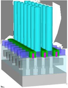


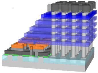

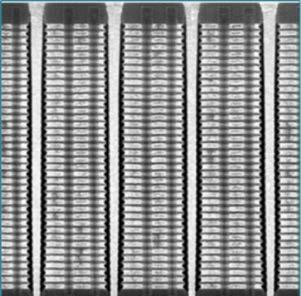

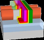


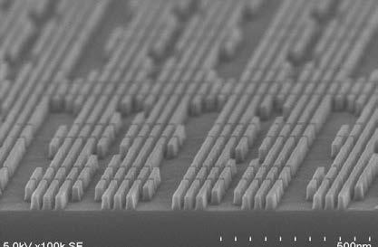
4 Patterning Destination Set by Device Technology DRAM 3D NAND Logic Planar STI PMOS T. Ghani, et al., IEDM Dry Exposure FinFET STI 22nm (FinFET RMG) C. Auth, et al., VLSI tech SADP + Cut (x1 2) Nanowire STI SEM Image : TEL AR > 50 Jae-woo Im et al., ISSCC, 201 R. Coquand et al., VLSI tech SAQP + Cut (x2 3) 4


5 Patterning Paths Which to Choose? EUV Multiple Patterning DSA Source: IMEC 2015 Process Simplicity Design Flexibility Pitch Scalability Production Ready Low CapEx Materials Enabled Shrink High CapEx Tool Productivity Edge Placement Error (EPE) Process Complexity Self Alignment Defect Design Flexibility 5


6 Patterning at a Crossroads 6

7 Immersion Multiple Patterning Patterning Superhighway Gate Fin Metal 7

 Planarization Etch Line Cut Etch Deposition Key Patterning")

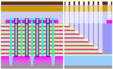
8 Immersion Multiple Patterning Process Pre Pattern Grid Formation Cut Pattern Pattern Memorization Critical Process Step 193i Single Patterning Litho Material Process SAMP (DP, QP, OP) Deposition Etch LE x Multiple Patterning Litho (193i, EUV) Planarization Etch Line Cut Etch Deposition Key Patterning Technology LER Reduction CDU Control LER Reduction CDU Control Spacer Selectivity Hole Shrink Pattern Healing Variation Control Self Alignment Pattern Reversal HM Selectivity 8


 PR")
9 Grid Pattern Formation DCS & Metal Oxide Spacer SiO 2 SADP Performance Enhancements Direct Current Superposition (DCS) Technology Photo Resist TiO SiARC Ar + EB H* DCS cured (Enhanced Smoothing) PR Curing Si Si Si TiO Spacer (Improved Selectivity) Si Coating 9


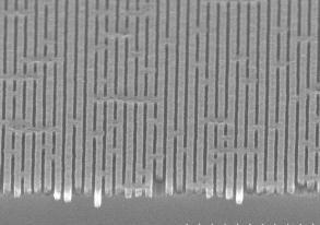
10 Grid Pattern Formation DCS & Metal Oxide Spacer 44nm hp Photo Resist 22nm hp Spacer Depo Spacer RIE Middle Layer RIE Bottom Layer RIE Ox spacer DCS applied TiO spacer Improved LER & Resist Profile No recess on Middle Layer Higher RIE Selectivity Improved Image Transfer Low temperature TiO and DCS process enable improved SADP process 10


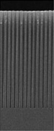
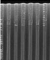
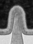
11 Cut Pattern Formation Healing & Shrinking For Fin, Gate 193i 41.9nm 17.5nm 18.7nm Trench shrink for cutmask 20.0LS 66.1nm 19.9nm 19.8nm Hole shrink Hole multiplication 11.8LS For Via, Contact 63nm 63nm 63nm 14nmΦ 63nm 11


12 Cut Pattern Formation Healing & Shrinking Min 63nm pitch in immersion PR SiARC SOC TEOS In-situ polymer deposition thru-etching SiARC etch SOC etch Oxide etch Ashing 63nm 63nm 63nm 14nmΦ 63nm 12
 25 20 15 10 5 0")

 0 50 100 DOF (nm) CER (nm) 6 5")
 60 55 50 45 40 CER 3.")
")

")


13 Cut Pattern Formation Healing & Shrinking EL (%) Nominal dose best focus Under dose defocus Process Window ADI (49.3nm±10%) AEI (31.2m±10%) DOF (nm) CER (nm) Hole CD Healing CDU 15.5nm (3sig) CER 3.6nm hole CD(nm) nm nm Placement error Y (nm) Placement Error ADI Placement error X (nm) 8 Placement error Y (nm) 6 Design based AEI Placement error X (nm) EL: 60% enlarged DOF: 34% enlarged CDU: 80% improved CER: 70% improved *CER: Circle Edge Roughness Keep Placement Error TEL healing & shrinking improves overall process variability 13

14 \ EUV Patterning Waiting for the Light 14

 FIRM Extreme TM FIRM Extreme TM A Process Window Count 18 21")
 6.4 6.2 5.")

15 Pattern Collapse Mitigation at 22nm HP Process Condition Exposure tool: NXE3100 Resist: ESR1 Process: 2.38% TMAH DIW rinse Surfactant rinse DIW (ref.) FIRM Extreme TM FIRM Extreme TM A Process Window Count Resolution Limit (nm) Sensitivity at 22nm (mj/cm2) LWR at 22nm (nm) Pattern Size 22nm Half pitch (Top-Down SEM Image) Resolution and LER improvement achieved using surfactant rinse FIRM Extreme A FIRM Extreme is a trademark of Merck Performance Materials 15


16 CLEAN TRACK LWR & CER Improvement 70nm pitch/ line and space 64nm pitch/ line and space 56nm pitch/ line and space 44nm pitch/ line and space 64nm pitch/ contact hole Presmoothing LWR 5.20nm LWR 4.42nm LWR 5.48nm LWR 7.03nm CER 1.84nm Postsmoothing LWR 4.66nm LWR 3.90nm LWR 4.74nm LWR 6.23nm CER 1.59nm 10.3% Improved 11.8% Improved 13.5% Improved 11.3% Improved 13.8% Improved TEL Jun Sung Chun / SEMATECH et. al, SPIE2014 TEL vapor phase smoothing process can improve LWR and CER 16


17 Etch Hardening & LER Improvement Post Litho CD 29nm No Cure CD 38nm Post Etch w/cure CD 37nm 13.5nm EUV Resist Base FTIR Data for cured & un-cured resist LER 2.9nm LER 2.2nm LER 1.8nm CD 63nm CD 52nm CD 53nm LER 3.5nm LER 2.9nm LER 2.5nm VUV cure can modify chemical structure of EUV resist leading to smoothing ~ 20-30% improvement in roughness for optimized cure process as compared to non-cure 17


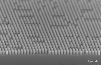
18 DSA Patterning Order From Chaos Self-Aligned L/S Pitch Multiplication Self-Aligned Hole Pitch Multiplication Simple Pitch Multiplication with CDU/LWR Self-Healing 18

19 DSA Hole Shrink Process Flow Hole Guide Affinity Control BCP Coat & Bake PMMA Wet Dev. Negative tone resist pattern Affinity control processes to change template surface properties Wet development removes PMMA core 19


20 Champion Hole Defectivity 2015 CLEAN TRACK LITHIUS Pro Z DSA Normalized Defect Density Others 39% DSA Failure 9% On Material 25% Missing Hole 27% Q1/13 Q2/13 Q4/13 Q1/14 Q3/14 Missing Hole Large Material Small Material Embedded DSA Failure Line Signature Others 20


![6nm LWR: 2.11nm LER: 1.98nm LER, LWR [nm] 6.0 5.0 4.0 3.](/docs-images/72/66924731/images/21-3.jpg "0 2.0 1.0 6.0 5.0 4.0 3.0 2.0 1.0 Selectivity X-SEM SiARC remain: 15.")

![0 0 200 400 600 800 HF Source Power [W] Effect of Ion](/docs-images/72/66924731/images/21-5.jpg "Energy LER LWR Selectivity 6.")

21 DSA Etch Overall Process Optimization Position Center Right Middle Right Edge Effect of HF RF Power LER LWR Selectivity CD-SEM Square scan 300K CD: 21.5nm LWR: 1.84nm LER: 1.79nm CD: 21.9nm LWR: 1.94nm LER: 2.07nm CD: 21.6nm LWR: 2.11nm LER: 1.98nm LER, LWR [nm] Selectivity X-SEM SiARC remain: 15.5nm Btm CD: 23.5nm SiARC remain: 20.9nm Btm CD: 25.1nm SiARC remain: 13.7nm Btm CD: 24.3nm HF Source Power [W] Effect of Ion Energy LER LWR Selectivity 6.0 Simultaneous optimization of CDU, LER, and selectivity achieved LER, LWR [nm] Selectivity Vpp [V] 21

22 Crossroads or Converging Paths? 22
23 Summary New drivers for increased computing power and storage continue to demand new semiconductor technologies Traditional scaling is at an inflection point, requiring new innovation to enable cost effective patterning solutions Developing these innovations requires partnership between customers, consortia, and suppliers TEL is ready to support all patterning technologies 23


24 What path do you want to follow? TEL Patterning Solutions 謝謝 TM 24
25 Acknowledgements Semiconductor companies collaborations Consortia (EIDEC, IMEC, SEMATECH) Material suppliers (Merck, TOK) Equipment suppliers (ASML, HHT, KLA-Tencor) TEL global technology teams (PSP, TDC, ATG, TTCA) Co-authors Hidetami Yaegashi Kenichi Oyama Takashi Hayakawa Takahiro Kitano Makoto Muramatsu Kousuke Yoshihara Satoru Shimura Shinichiro Kawakami Toshikatsu Tobana Mark Somervell Carlos Fonseca Ben Rathsack Anton devilliers Serge Biesmans Omar Madrigal Samuel House Rob Crowell Nagisa Sato Ken Nawa Koichi Yatsuda Seiji Fujimoto Noritaka Yokomori Hideo Nakashima Seiji Nagahara Hiroyuki Iwaki Akihiro Sonoda TEL is a trademark of Tokyo Electron Limited. steven1.scheer@tel.com 25
Self-Aligned Double Patterning for 3xnm Flash Production
 Self-Aligned Double Patterning for 3xnm Flash Production Chris Ngai Dir of Process Engineering & Lithography Maydan Technology Center Group Applied Materials, Inc. July 16 th, 2008 Overview Double Patterning
COMPARISON OF EUV SINGLE EXPOSURE VS. 193i MULTIPLE PATTERING FOR N10 BEOL CHRISTOPHER J. WILSON
 COMPARISON OF EUV SINGLE EXPOSURE VS. 193i MULTIPLE PATTERING FOR N10 BEOL CHRISTOPHER J. WILSON - CONTRIBUTORS FORM ADVANCED LITHO AND CU-LOW-K IIAP PROGRAMS - ASML VELDHOVEN DEMO LAB FOR EXPOSURES EUV
Readiness and Challenges of EUV Mask
 Panel Discussion: EUVL HVM Insertion and Scaling Readiness and Challenges of EUV Mask Takashi Kamo Toshiba Corporation Semiconductor & Storage Products Company Contents [1] Introduction [2] EUV Mask Defect
SEMICON Europe October Pushing Lithography to the Limits. Patrick Wong imec
 SEMICON Europe October 2009 Pushing Lithography to the Limits imec 2009 1 Alternative double patterning processes : ready for (sub) 32nm hp? P. Wong, M. Maenhoudt, D. Vangoidsenhoven, V. Wiaux Outline
Outline. Double Patterning 11/6/17. Motivation Techniques Future of Double Patterning. Rasha El-Jaroudi November 7 th
 Double Patterning Rasha El-Jaroudi November 7 th 2017 reljaroudi@utexas.edu Outline Motivation Techniques Future of Double Patterning Rasha H. El-Jaroudi 2 1 Motivation Need to keep up with Moore s Law
UV Nanoimprint Tool and Process Technology. S.V. Sreenivasan December 13 th, 2007
 UV Nanoimprint Tool and Process Technology S.V. Sreenivasan December 13 th, 2007 Agenda Introduction Need tool and process technology that can address: Patterning and CD control Alignment and Overlay Defect
SEMICONDUCTOR TECHNOLOGY -CMOS-
 SEMICONDUCTOR TECHNOLOGY -CMOS- Fire Tom Wada What is semiconductor and LSIs Huge number of transistors can be integrated in a small Si chip. The size of the chip is roughly the size of nails. Currently,
SEMICONDUCTOR TECHNOLOGY -CMOS-
 SEMICONDUCTOR TECHNOLOGY -CMOS- Fire Tom Wada 2011/12/19 1 What is semiconductor and LSIs Huge number of transistors can be integrated in a small Si chip. The size of the chip is roughly the size of nails.
Nano-Imprint Lithography Infrastructure: Imprint Templates
 Nano-Imprint Lithography Infrastructure: Imprint Templates John Maltabes Photronics, Inc Austin, TX 1 Questions to keep in mind Imprint template manufacturability Resolution Can you get sub30nm images?
DOUBLE PATTERNING CHALLENGES FOR 20nm TECHNOLOGY
 DOUBLE PATTERNING CHALLENGES FOR 20nm TECHNOLOGY SEMICON DRESDEN TechARENA OCTOBER 12 th 2011 Vincent Farys, Bertrand Le-Gratiet, Pierre-Jérôme Goirand STMicroelectronics Crolles 2 OUTLINE Lithography
Selective isotropic etching of Group IV semiconductors to enable gate all around device architectures
 TEL Technology Center, America, LLC - imec Selective isotropic etching of Group IV semiconductors to enable gate all around device architectures SPCC, April 10, 2018 S. Kal 1, C. Pereira 1, Y. Oniki 2,
Defect Reduction for Semiconductor Memory Applications Using Jet And Flash Imprint Lithography
 Defect Reduction for Semiconductor Memory Applications Using Jet And Flash Imprint Lithography Zhengmao Ye, Kang Luo, Xiaoming Lu, Brian Fletcher, Weijun Liu, Frank Xu, Dwayne LaBrake, Douglas Resnick,
The Transition to Patterned Media in Hard Disk Drives
 The Transition to Patterned Media in Hard Disk Drives The Evolution of Jet and Flash Imprint Lithography for Patterned Media DISKCON San Jose Sept 24 rd, 2009 Paul Hofemann, Vice President, HDD Future
PROGRESS OF UV-NIL TEMPLATE MAKING
 PROGRESS OF UV-NIL TEMPLATE MAKING Takaaki Hiraka, Jun Mizuochi, Yuko Nakanishi, Satoshi Yusa, Shiho Sasaki, Yasutaka Morikawa, Hiroshi Mohri, and Naoya Hayashi Electronic Device Laboratory, Dai Nippon
ABSTRACT. Keywords: 3D NAND, FLASH memory, Channel hole, Yield enhancement, Defect inspection, Defect reduction DISCUSSION
 Yield enhancement of 3D flash devices through broadband brightfield inspection of the channel hole process module Jung-Youl Lee a, Il-Seok Seo a, Seong-Min Ma a, Hyeon-Soo Kim a, Jin-Woong Kim a DoOh Kim
Scalable self-aligned active matrix IGZO TFT backplane technology and its use in flexible semi-transparent image sensors. Albert van Breemen
 Scalable self-aligned active matrix IGZO TFT backplane technology and its use in flexible semi-transparent image sensors Albert van Breemen Image sensors today 1 Dominated by silicon based technology on
Defense Technical Information Center Compilation Part Notice
 UNCLASSIFIED Defense Technical Information Center Compilation Part Notice ADPO1 1322 TITLE: Amorphous- Silicon Thin-Film Transistor With Two-Step Exposure Process DISTRIBUTION: Approved for public release,
Advanced Display Manufacturing Technology
 Advanced Display Manufacturing Technology John Busch Vice President, New Business Development Display and Flexible Technology Group September 28, 2017 Safe Harbor This presentation contains forward-looking
Semiconductors Displays Semiconductor Manufacturing and Inspection Equipment Scientific Instruments
 Semiconductors Displays Semiconductor Manufacturing and Inspection Equipment Scientific Instruments Electronics 110-nm CMOS ASIC HDL4P Series with High-speed I/O Interfaces Hitachi has released the high-performance
Double Patterning OPC and Design for 22nm to 16nm Device Nodes
 Double Patterning OPC and Design for 22nm to 16nm Device Nodes Kevin Lucas, Chris Cork, Alex Miloslavsky, Gerry Luk-Pat, Xiaohai Li, Levi Barnes, Weimin Gao Synopsys Inc. Vincent Wiaux IMEC 1 Outline Introduction
Transforming Electronic Interconnect Breaking through historical boundaries Tim Olson Founder & CTO
 Transforming Electronic Interconnect Breaking through historical boundaries Tim Olson Founder & CTO Remember when? There were three distinct industries Wafer Foundries SATS EMS Semiconductor Devices Nanometers
Recent results of Multi-beam mask writer MBM-1000
 Recent results of Multi-beam mask writer MBM-1000 Hiroshi Matsumoto, Hiroshi Yamashita, Hideo Inoue, Kenji Ohtoshi, Hirokazu Yamada Member of the ebeam Initiative 1 NFT s mask writer roadmap 2016 Device
AMOLED Manufacturing Process Report SAMPLE
 AMOLED Manufacturing Process Report SAMPLE 2018 AMOLED Manufacturing Process Report The report analyzes the structure and manufacturing process by dividing AMOLED into small & medium-sized rigid OLED,
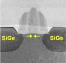
Pre SiGe Wet Cleans Development for sub 1x nm Technology Node
 Pre SiGe Wet Cleans Development for sub 1x nm Technology Node Akshey Sehgal, Anand Kadiyala, Michael DeVre and, Norberto Oliveria April 10 th, 2018 Background Due to higher aspect ratio features observed
CMP and Current Trends Related to Advanced Packaging
 CMP and Current Trends Related to Advanced Packaging Robert L. Rhoades, Ph.D. NCCAVS TFUG-CMPUG Joint Meeting June 7, 2017 Semiconductor Equipment Spare Parts and Service CMP Foundry Foundry Click to edit
Study of Pattern Area Reduction. with FinFET and SGT for LSI
 Contemporary Engineering Sciences, Vol. 6, 2013, no. 4, 177-190 HIKRI Ltd, www.m-hikari.com Study of Pattern rea Reduction with FinFET and SGT for LSI Takahiro Kodama Japan Process Development Co., Ltd.
IC TECHNOLOGY Lecture 2.
 IC TECHNOLOGY Lecture 2. IC Integrated Circuit Technology Integrated Circuit: An integrated circuit (IC, a chip, or a microchip) is a set of electronic circuits on one small flat piece (or "chip") of semiconductor
Advances in Roll-to-Roll Imprint Lithography for Display Applications Using Self Aligned Imprint Lithography. John G Maltabes HP Labs
 Advances in Roll-to-Roll Imprint Lithography for Display Applications Using Self Aligned Imprint Lithography John G Maltabes HP Labs Outline Introduction Roll to Roll Challenges and Benefits HP Labs Roll
New Worlds for Polymers: Organic Transistors, Light Emitting Diodes, and Optical Waveguides Ed Chandross
 New Worlds for Polymers: Organic Transistors, Light Emitting Diodes, and Optical Waveguides Ed Chandross Materials Chemistry, LLC 1 Polymers in the Electronic Industry Enabling Materials Active Materials?
Applied Materials. 200mm Tools & Process Capabilities For Next Generation MEMS. Dr Michel (Mike) Rosa
 Rosa") Applied Materials 200mm Tools & Process Capabilities For Next Generation MEMS Dr Michel (Mike) Rosa 200mm MEMS Global Product / Marketing Manager, Components and Systems Group (CSG), Applied Global Services
Applied Materials 200mm Tools & Process Capabilities For Next Generation MEMS Dr Michel (Mike) Rosa 200mm MEMS Global Product / Marketing Manager, Components and Systems Group (CSG), Applied Global Services
Approaching Zero Etch Bias at Cr Etch Process
 Approaching Zero Etch Bias at Cr Etch Process Pavel Nesladek a ; Norbert Falk b ; Andreas Wiswesser a ; Renee Koch b ; Björn Sass a a Advanced Mask Technology Center, Rähnitzer Allee 9; 01109 Dresden,
~ 50, ,000 ~ $500K
 Mask Replication The lifetime of a mask is anticipated to be ~ 50,000 100,000 imprints An e-beam written master mask will cost ~ $500K If you wanted to print 1M wafers, you would spend ~ $500M on masks
The Challenges in Making NIL Master Templates
 The Challenges in Making NIL Master Templates Naoya Hayashi Dai Nippon Printing Co., Ltd. A Member of the ebeam Initiative 2011 Dai Nippon Printing Co.,Ltd. All Rights Reserved. OUTLINE Recent Progress
Next Generation of Poly-Si TFT Technology: Material Improvements and Novel Device Architectures for System-On-Panel (SOP)
") Next Generation of Poly-Si TFT Technology: Material Improvements and Novel Device Architectures for System-On-Panel (SOP) Tolis Voutsas* Paul Schuele* Bert Crowder* Pooran Joshi* Robert Sposili* Hidayat
Next Generation of Poly-Si TFT Technology: Material Improvements and Novel Device Architectures for System-On-Panel (SOP) Tolis Voutsas* Paul Schuele* Bert Crowder* Pooran Joshi* Robert Sposili* Hidayat
Because Innovation Matters
 Because Innovation Matters Silicon Systems Group Toru Watanabe President, Applied Materials, Japan Semicon Japan November 30, 2010 Safe Harbor This presentation contains forward-looking statements, including
Wafer Thinning and Thru-Silicon Vias
 Wafer Thinning and Thru-Silicon Vias The Path to Wafer Level Packaging jreche@trusi.com Summary A new dry etching technology Atmospheric Downstream Plasma (ADP) Etch Applications to Packaging Wafer Thinning
Overcoming Challenges in 3D NAND Volume Manufacturing
 Overcoming Challenges in 3D NAND Volume Manufacturing Thorsten Lill Vice President, Etch Emerging Technologies and Systems Flash Memory Summit 2017, Santa Clara 2017 Lam Research Corp. Flash Memory Summit
Abstract. Keywords INTRODUCTION. Electron beam has been increasingly used for defect inspection in IC chip
 Abstract Based on failure analysis data the estimated failure mechanism in capacitor like device structures was simulated on wafer in Front End of Line. In the study the optimal process step for electron
Leveraging 300 mm Technology Solutions to Enable New MEMS Process Capabilities
 Leveraging 300 mm Technology Solutions to Enable New MEMS Process Capabilities Evan Patton Semicon Europa November 2017 Lam Research Corp. 1 Presentation Outline The Internet of Things (IoT) as a market
FinFETs & SRAM Design
 FinFETs & SRAM Design Raymond Leung VP Engineering, Embedded Memories April 19, 2013 Synopsys 2013 1 Agenda FinFET the Device SRAM Design with FinFETs Reliability in FinFETs Summary Synopsys 2013 2 How
24. Scaling, Economics, SOI Technology
 24. Scaling, Economics, SOI Technology Jacob Abraham Department of Electrical and Computer Engineering The University of Texas at Austin VLSI Design Fall 2017 December 4, 2017 ECE Department, University
Methodology for Trench Capacitor Etch Optimization using Voltage Contrast Inspection and Special Processing
 Methodology for Trench Capacitor Etch Optimization using Voltage Contrast Inspection and Special Processing 1 Oliver D. Patterson, 1 Xing J. Zhou, 1 Rohit S. Takalkar, 1 Katherine V. Hawkins, 1 Eric H.
Removing the Last Road Block of Deploying ILT into 10nm Node by Model-based Mask Data Preparation and Overlapped Shots
 Removing the Last Road Block of Deploying ILT into 10nm Node by Model-based Mask Data Preparation and Overlapped Shots Linyong (Leo) Pang Bo Su, Yohan Choi D2S, Inc. 1 193i Needed to be Extended and Extended
Automation in Semiconductor Manufacturing IEDM, San Francisco, 1982 Keynote Speech
 Automation in Semiconductor Manufacturing IEDM, San Francisco, 1982 Keynote Speech Commentary Alongside ISSCC, IEDM is the most traditional academic conference in the semiconductor field, and it is held
Deep Silicon Etch Technology for Advanced MEMS Applications
 Deep Silicon Etch Technology for Advanced MEMS Applications Shenjian Liu, Ph.D. Managing Director, AMEC AMEC Company Profile and Product Line-up AMEC HQ, R&D and MF Facility in Shanghai AMEC Taiwan AMEC
Inspection of 32nm imprinted patterns with an advanced e-beam inspection system
 Inspection of 32nm imprinted patterns with an advanced e-beam inspection system Hong Xiao, Long (Eric) Ma, Fei Wang, Yan Zhao, and Jack Jau Hermes Microvision, Inc., 1762 Automation Parkway, San Jose,
Controlling Linewidth Roughness in Step and Flash Imprint Lithography
 Controlling Linewidth Roughness in Step and Flash Imprint Lithography Gerard M. Schmid a, Niyaz Khusnatdinov a, Cynthia B. Brooks a, Dwayne LaBrake a, Ecron Thompson a, Douglas J. Resnick a *, Jordan Owens
Lower BW and its impact on the patterning performance
 Lower BW and its impact on the patterning performance Paolo Alagna a, Greg Rechtsteiner b, Vadim Timoshkov c, Patrick Wong d Will Conley b, Jan Baselmans c a) Cymer LLC, Kapeldreef 75, 3001 Leuven, Belgium
Fabrication of Step and Flash TM Imprint Lithography Templates Using Commercial Mask Processes
 Fabrication of Step and Flash TM Imprint Lithography Templates Using Commercial Mask Processes Ecron Thompson, Peter Rhyins, Ron Voisin, S.V. Sreenivasan *, Patrick Martin Molecular Imprints, Inc., 1807C
Model-Based Mask Data Preparation (MB-MDP) and its impact on resist heating
 and its impact on resist heating") Model-Based Mask Data Preparation (MB-MDP) and its impact on resist heating Aki Fujimura* a, Takashi Kamikubo b, Ingo Bork a a D2S Inc., 4040 Moorpark Ave, Suite 250, San Jose, CA, 95117, USA; b NuFlare
Model-Based Mask Data Preparation (MB-MDP) and its impact on resist heating Aki Fujimura* a, Takashi Kamikubo b, Ingo Bork a a D2S Inc., 4040 Moorpark Ave, Suite 250, San Jose, CA, 95117, USA; b NuFlare
EECS150 - Digital Design Lecture 2 - CMOS
 EECS150 - Digital Design Lecture 2 - CMOS January 23, 2003 John Wawrzynek Spring 2003 EECS150 - Lec02-CMOS Page 1 Outline Overview of Physical Implementations CMOS devices Announcements/Break CMOS transistor
AIXTRON in EXCILIGHT project
 AIXTRON SE AIXTRON in EXCILIGHT project Gintautas Simkus ABOUT AIXTRON 2 Who we are Headquarter based in Herzogenrath, Germany Worldwide presence with 14 sales/representatives offices and production facilities
Layout Analysis Analog Block
 Layout Analysis Analog Block Sample Report Analysis from an HD Video/Audio SoC For any additional technical needs concerning semiconductor and electronics technology, please call Sales at Chipworks. 3685
Introduction and recent results of Multi-beam mask writer MBM-1000
 Introduction and recent results of Multi-beam mask writer MBM-1000 Hiroshi Matsumoto, Yasuo Kato, Munehiro Ogasawara, Hirokazu Yamada February 23 rd, 2016 Member of the ebeam Initiative NFT s mask writer
Digital Integrated Circuits EECS 312
 14 12 10 8 6 Fujitsu VP2000 IBM 3090S Pulsar 4 IBM 3090 IBM RY6 CDC Cyber 205 IBM 4381 IBM RY4 2 IBM 3081 Apache Fujitsu M380 IBM 370 Merced IBM 360 IBM 3033 Vacuum Pentium II(DSIP) 0 1950 1960 1970 1980
Advanced Sensor Technologies
 Advanced Sensor Technologies Jörg Amelung Fraunhofer Institute for Photonics Microsystems Name of presenter date Sensors as core element for IoT Next phase of market grow New/Advanced Requirements based
Digital Integrated Circuits EECS 312. Review. Remember the ENIAC? IC ENIAC. Trend for one company. First microprocessor
 14 12 10 8 6 IBM ES9000 Bipolar Fujitsu VP2000 IBM 3090S Pulsar 4 IBM 3090 IBM RY6 CDC Cyber 205 IBM 4381 IBM RY4 2 IBM 3081 Apache Fujitsu M380 IBM 370 Merced IBM 360 IBM 3033 Vacuum Pentium II(DSIP)
Solution-based transistor matrix
 18 PRINTED ELECTRONICS Solution-based transistor matrix A groundbreaking new technology is making it far more cost-effective to produce the electronic control unit of liquid crystal displays. At the same
Advancements in Acoustic Micro-Imaging Tuesday October 11th, 2016
 Central Texas Electronics Association Advancements in Acoustic Micro-Imaging Tuesday October 11th, 2016 A review of the latest advancements in Acoustic Micro-Imaging for the non-destructive inspection
Flexible Electronics Production Deployment on FPD Standards: Plastic Displays & Integrated Circuits. Stanislav Loboda R&D engineer
 Flexible Electronics Production Deployment on FPD Standards: Plastic Displays & Integrated Circuits Stanislav Loboda R&D engineer The world-first small-volume contract manufacturing for plastic TFT-arrays
BTC and SMT Rework Challenges
 BTC and SMT Rework Challenges Joerg Nolte Ersa GmbH Wertheim, Germany Abstract Rising customer demands in the field of PCB repair are a daily occurrence as the rapid electronic industry follows new trends
RFSOI and FDSOI enabling smarter and IoT applications. Kirk Ouellette Digital Products Group STMicroelectronics
 RFSOI and FDSOI enabling smarter and IoT applications Kirk Ouellette Digital Products Group STMicroelectronics ST in the IoT already Today 2 Kirk Ouellette More then Moore Workshop - Shanghai - March 17,
1. Publishable summary
 1. Publishable summary 1.1. Project objectives. The target of the project is to develop a highly reliable high brightness conformable low cost scalable display for demanding applications such as their
High Performance Microprocessor Design and Automation: Overview, Challenges and Opportunities IBM Corporation
 High Performance Microprocessor Design and Automation: Overview, Challenges and Opportunities Introduction About Myself What to expect out of this lecture Understand the current trend in the IC Design
Etching Part 2. Saroj Kumar Patra. TFE4180 Semiconductor Manufacturing Technology. Norwegian University of Science and Technology ( NTNU )
") 1 Etching Part 2 Chapter : 16 Semiconductor Manufacturing Technology by M. Quirk & J. Serda Spring Semester 2014 Saroj Kumar Patra, Norwegian University of Science and Technology ( NTNU ) 2 Introduction
1 Etching Part 2 Chapter : 16 Semiconductor Manufacturing Technology by M. Quirk & J. Serda Spring Semester 2014 Saroj Kumar Patra, Norwegian University of Science and Technology ( NTNU ) 2 Introduction
Freescale SPC5604BF1CLL6 Embedded NOR Flash with M27V Die Markings 32 Bit Power Architecture Automotive Microcontroller 90 nm Logic Process
 Freescale SPC5604BF1CLL6 Embedded NOR Flash with M27V Die Markings 32 Bit Power Architecture Automotive Microcontroller 90 nm Logic Process Process Review 3685 Richmond Road, Suite 500, Ottawa, ON K2H
QPA2626D GHz Low Noise Amplifier
 Product Overview Qorvo s QPAD is a high-performance, low noise MMIC amplifier fabricated on Qorvo s production 9nm phemt process (QPHT9). Covering 17 23 GHz, the QPAD provides 25 db small signal gain and
Emerging Memory Technologies
 Report No. FI-NVM-EMT-1209 By: Josef Willer, Gregory Wong December 2009 2009 Forward Insights. All Rights Reserved. Reproduction and distribution of this publication in any form in whole or in part without
FS3 Series Tri-Lens for SEOUL SEMICONDUCTOR Z-POWER P4 TM LEDs
 FS3 Series Tri-Lens for SEOUL SEMICONDUCTOR Z-POWER P4 TM LEDs High efficiency 3 beams available MR-16 size tri-lens The FS3 tri-lens offers MR16 size lenses specifically designed for the Seoul Semiconductor
STMicroelectronics NAND128W3A2BN6E 128 Mbit NAND Flash Memory Structural Analysis
 July 6, 2006 STMicroelectronics NAND128W3A2BN6E Structural Analysis For comments, questions, or more information about this report, or for any additional technical needs concerning semiconductor technology,
How UV selectable illumination inspection tool and methodologies can accelerate learning curve of advanced technologies
 How UV selectable illumination inspection tool and methodologies can accelerate learning curve of advanced technologies V. Twines, C. Archambuult, B. Hinschberger, E. Rouchouze ST Microelectronic Crolles
Industrial Inline Control for Advanced Vacuum Roll to Roll Systems. Gerhard Steiniger Web inspection - surface Quallity control 7.
 Industrial Inline Control for Advanced Vacuum Roll to Roll Systems Gerhard Steiniger Web inspection - surface Quallity control 7.4-7684 1 Industrial Inline Control for Advanced Vacuum Roll to Roll Systems
WAH WANG HOLDINGS (HONG KONG) CO., LTD.
 CO., LTD.") Wah Wang Data Sheet For 5mm Super Flux White LED High Reliable Type High Power 3 LED Chips Series RF-M05V53WUR4-B4-Q Address : Unit C, D & E, 12/F., Po Shau Centre, No. 115 How Ming Street Kwun Tong, Kowloon,
Wah Wang Data Sheet For 5mm Super Flux White LED High Reliable Type High Power 3 LED Chips Series RF-M05V53WUR4-B4-Q Address : Unit C, D & E, 12/F., Po Shau Centre, No. 115 How Ming Street Kwun Tong, Kowloon,
Lecture 1: Intro to CMOS Circuits
 Introduction to CMOS VLSI esign Lecture : Intro to CMOS Circuits avid Harris Steven Levitan Fall 28 Harvey Mudd College Spring 24 Outline A Brief History CMOS Gate esign Pass Transistors CMOS Latches &
DESIGN AND SIMULATION OF LOW POWER JK FLIP-FLOP AT 45 NANO METER TECHNOLOGY
 DESIGN AND SIMULATION OF LOW POWER JK FLIP-FLOP AT 45 NANO METER TECHNOLOGY 1 Anshu Mittal, 2 Jagpal Singh Ubhi Department of Electronics and Communication Engineering, Sant Longowal Institute of Engineering
I-fuse TM : Best OTP for FD-SOI and Sub-14nm
 I-fuse TM : Best OTP for FD-SOI and Sub-14nm Shine Chung, Chairman May, 2017 Attopsemi Technology 1A2-A1 No. 1 Li-Hsin 1st Rd, Hsinchu, Taiwan 300-76 (886) 3-666-3150x211, (886) 920-566-218 1 1 About Attopsemi
High-Performance Technologies for an Analog-Centric World
 High-Performance Technologies for an Analog-Centric World Oct 13, 2011 Lou N. Hutter, SVP GM, Analog Foundry Business Unit Dongbu HiTek Agenda Analog in Our World Today Diverse Technology Needs of the
Summary of Selected EMCR650 Projects for Fall 2005 Mike Aquilino Dr. Lynn Fuller
 ROCHESTER INSTITUTE OF TECHNOLOGY MICROELECTRONIC ENGINEERING Summary of Selected EMCR650 Projects for Fall 2005 Mike quilino Dr. Lynn Fuller http://www.rit.edu/~lffeee 82 Lomb Memorial Drive Rochester,
CCD 143A 2048-Element High Speed Linear Image Sensor
 A CCD 143A 2048-Element High Speed Linear Image Sensor FEATURES 2048 x 1 photosite array 13µm x 13µm photosites on 13µm pitch High speed = up to 20MHz data rates Enhanced spectral response Low dark signal
21 rue La Noue Bras de Fer Nantes - France Phone : +33 (0) website :
 website :") 21 rue La Noue Bras de Fer - 44200 Nantes - France Phone : +33 (0) 240 180 916 - email : info@systemplus.fr - website : www.systemplus.fr 2012 September - Version 1 Written by: Maher Sahmimi DISCLAIMER
21 rue La Noue Bras de Fer - 44200 Nantes - France Phone : +33 (0) 240 180 916 - email : info@systemplus.fr - website : www.systemplus.fr 2012 September - Version 1 Written by: Maher Sahmimi DISCLAIMER
OLED Status quo and our position
 OLED Status quo and our position Information Day 2013 A Deep Dive into the LC&OLED Business Dr. Udo Heider Vice President OLED Darmstadt, Germany June 26, 2013 Disclaimer Remarks All comparative figures
Defense Technical Information Center Compilation Part Notice
 UNCLASSIFIED Defense Technical Information Center Compilation Part Notice ADPO 11305 TITLE: Advanced Manufacturing Technologies on Color Plasma Displays DISTRIBUTION: Approved for public release, distribution
Lossless Compression Algorithms for Direct- Write Lithography Systems
 Lossless Compression Algorithms for Direct- Write Lithography Systems Hsin-I Liu Video and Image Processing Lab Department of Electrical Engineering and Computer Science University of California at Berkeley
Challenges for OLED Deposition by Vacuum Thermal Evaporation. D. W. Gotthold, M. O Steen, W. Luhman, S. Priddy, C. Counts, C.
 Challenges for OLED Deposition by Vacuum Thermal Evaporation D. W. Gotthold, M. O Steen, W. Luhman, S. Priddy, C. Counts, C. Roth June 7, 2011 Outline Introduction to Veeco Methods of OLED Deposition Cost
Layers of Innovation: How Signal Chain Innovations are Creating Analog Opportunities in a Digital World
 The World Leader in High Performance Signal Processing Solutions Layers of Innovation: How Signal Chain Innovations are Creating Analog Opportunities in a Digital World Dave Robertson-- VP of Analog Technology
LEP400 Etch Depth Monitor Real-time, in-situ plasma etch depth monitoring and end point control plus co-linear wafer vision system
 LEP400 Etch Depth Monitor Real-time, in-situ plasma etch depth monitoring and end point control plus co-linear wafer vision system Base Configuration Etch Depth Monitoring LEP400 Recessed Window Plasma
Product Specification PE613010
 Product Description The is an SPST tuning control switch based on Peregrine s UltraCMOS technology. This highly versatile switch supports a wide variety of tuning circuit topologies with emphasis on impedance
Principles of Electrostatic Chucks 6 Rf Chuck Edge Design
 Principles of Electrostatic Chucks 6 Rf Chuck Edge Design Overview This document addresses the following chuck edge design issues: Device yield through system uniformity and particle reduction; System
An Efficient IC Layout Design of Decoders and Its Applications
 An Efficient IC Layout Design of Decoders and Its Applications Dr.Arvind Kundu HOD, SCIENT Institute of Technology. T.Uday Bhaskar, M.Tech Assistant Professor, SCIENT Institute of Technology. B.Suresh
WP36BHD T-1 (3mm) Blinking LED Lamp
 Blinking LED Lamp") T-1 (3mm) Blinking LED Lamp DESCRIPTIONS The Bright Red source color devices are made with Gallium Phosphide Red Light Emitting Diode Electrostatic discharge and power surge could damage the LEDs It is
T-1 (3mm) Blinking LED Lamp DESCRIPTIONS The Bright Red source color devices are made with Gallium Phosphide Red Light Emitting Diode Electrostatic discharge and power surge could damage the LEDs It is
SEMI 大半导体产业网
 STATE-OF-THE-ART 3D INTEGRATION GAN HUI, STEVEN OUTLINE Introduction about IMEC Application Areas Driven 3D Integration 3D Integration Technology Conclusions 1 IMEC 1984 2010 1984 Established by state
Spring Probes and Probe Cards for Wafer-Level Test. Jim Brandes Multitest. A Comparison of Probe Solutions for an RF WLCSP Product
 Session 6 AND, AT THE WAFER LEVEL For many in the industry, performing final test at the wafer level is still a novel idea. While providing some much needed solutions, it also comes with its own set of
9 rue Alfred Kastler - BP Nantes Cedex 3 - France Phone : +33 (0) website :
 website :") 9 rue Alfred Kastler - BP 10748-44307 Nantes Cedex 3 - France Phone : +33 (0) 240 180 916 - email : info@systemplus.fr - website : www.systemplus.fr January 2012 Written by: Maher SAHMIMI DISCLAIMER :
9 rue Alfred Kastler - BP 10748-44307 Nantes Cedex 3 - France Phone : +33 (0) 240 180 916 - email : info@systemplus.fr - website : www.systemplus.fr January 2012 Written by: Maher SAHMIMI DISCLAIMER :
Future trends for SiP In Medical Implant Applications
 Future trends for SiP In Medical Implant Applications Piers Tremlett, Zarlink Semiconductor NMI at TWI, 12 Dec 07 A case study This presentation uses Zarlink s Medical RF device To consider potential embedded
An Introduction to VLSI (Very Large Scale Integrated) Circuit Design
 Circuit Design") An Introduction to VLSI (Very Large Scale Integrated) Circuit Design Presented at EE1001 Oct. 16th, 2018 By Hua Tang The first electronic computer (1946) 2 First Transistor (Bipolar) First transistor Bell
An Introduction to VLSI (Very Large Scale Integrated) Circuit Design Presented at EE1001 Oct. 16th, 2018 By Hua Tang The first electronic computer (1946) 2 First Transistor (Bipolar) First transistor Bell
Cisco Video Surveillance 6050 IP Camera Data Sheet
 Data Sheet Cisco Video Surveillance 6050 IP Camera Data Sheet Product Overview The Cisco Video Surveillance 6050 IP Camera (shown in Figure 1) is a ruggedized, outdoor, high-definition video endpoint with
nmos transistor Basics of VLSI Design and Test Solution: CMOS pmos transistor CMOS Inverter First-Order DC Analysis CMOS Inverter: Transient Response
 nmos transistor asics of VLSI Design and Test If the gate is high, the switch is on If the gate is low, the switch is off Mohammad Tehranipoor Drain ECE495/695: Introduction to Hardware Security & Trust
Advanced MEMS Packaging
 Advanced MEMS Packaging John H. Lau Chengkuo Lee C. S. Premachandran Yu Aibin Ш New York Chicago San Francisco Lisbon London Madrid Mexico City Milan New Delhi San Juan Seoul Singapore Sydney Toronto Contents
FP 12.4: A CMOS Scheme for 0.5V Supply Voltage with Pico-Ampere Standby Current
 FP 12.4: A CMOS Scheme for 0.5V Supply Voltage with Pico-Ampere Standby Current Hiroshi Kawaguchi, Ko-ichi Nose, Takayasu Sakurai University of Tokyo, Tokyo, Japan Recently, low-power requirements are
Future of Analog Design and Upcoming Challenges in Nanometer CMOS
 Future of Analog Design and Upcoming Challenges in Nanometer CMOS Greg Taylor VLSI Design 2010 Outline Introduction Logic processing trends Analog design trends Analog design challenge Approaches Conclusion