High-Performance Technologies for an Analog-Centric World
|
|
|
- Spencer Greer
- 5 years ago
- Views:
Transcription

1 High-Performance Technologies for an Analog-Centric World Oct 13, 2011 Lou N. Hutter, SVP GM, Analog Foundry Business Unit Dongbu HiTek

2 Agenda Analog in Our World Today Diverse Technology Needs of the Analog Market High-Performance Analog Technologies Major Challenges in the Analog Roadmap Conclusions
3 2 Big Questions 1) The World is Going Digital, Right? 2) So Why am I Talking About Analog?


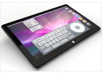
4 Fancy Smart Phones Apple iphone4 Samsung Galaxy


5 Apple iphone4 - A Closer Look Analog Power Audio Video Display Touch Transmitters Compass Logic/Memory Apps Processor + DRAM NAND Flash NOR Flash Quad Baseband Gyroscopes Accelerometer 9 Chips 4 Chips


6 Notebook A Closer Look Without Analog.. It won t TURN ON! The screen won t DISPLAY! Many other functions won t WORK (In case the 1st 2 problems weren t bad enough) Analog Inside


7 Analog is Everywhere Analog Semiconductor ICs
8 Answers to the 2 Big Questions 1) The World is Going Digital, Right? Yes 2) So Why am I Talking About Analog? Because the World s Going Digital But it needs Analog to get there!
9 What Did He Say???...A Closer Look Real World Signal Conditioning (Analog) The High Buzz Stuff Small Feature Sizes Temperature Pressure Position Motion Sound Video Light How to Electronically Interact With, and Control, This Real World? Signal Conditioning (Analog) Processor (Digital) The Low Buzz Stuff That Makes it Work
10 A Golf Analogy 1) You Drive for Show Logic/Memory and 2) You Putt for Dough Analog
11 Agenda Analog in Our World Today Diverse Technology Needs of the Analog Market High-Performance Analog Technologies Major Challenges in the Analog Roadmap Conclusions
12 Application Space Analog CMOS Automotive (Sensors) Baseband PMICs Audio Amplifiers (GP & HP) Data Converters (GP & HP) Power Automotive (Engine, ABS) LED Drivers & Lighting Class-D Audio Solar Micro-Inverters Motor Drivers Telecom, PoE
13 Digital vs. Analog Voltage Levels 1000V Electric Vehicles, Trains, Power Distribution LED Lighting, Industrial 100V 10V 1V Telecom, PoE Automotive, LED Drivers, Solar Hard Disk Drives, Industrial, Power Management Cell Phones, Power Management, Precision Analog Digital Logic 100mV Audio Signals 10mV Energy Harvesting Signals
14 Building an Analog Portfolio Analog IP & ESD Memory Functions High-Performance (Noise, TFR, PIP Caps) High-Voltage/Power (DECMOS, LDMOS, Power Metal) Analog CMOS Baseline (Logic CMOS, Analog CMOS, Passives, B/Gap Bipolar)
15 Agenda Analog in Our World Today Diverse Technology Needs of the Analog Market High-Performance Analog Technologies Major Challenges in the Analog Roadmap Conclusions
 Bipolar (NPN & PNP) JFETs Low CMOS 1/f Noise Low Resistor TCR Low Capacitor VCC & DA Component Matching Low Package Shifts Focus on Performance & Density Power BCD Automotive (Engine, ABS)")
16 Technology Care-Abouts Analog CMOS Automotive (Sensors) Logic CMOS Baseband Analog CMOS PMICs Poly or Thin-Film Resistor Audio PIP or MIM Cap Amplifiers (GP & HP) DECMOS (7V-30V) Data Converters (GP & HP) Bipolar (NPN & PNP) JFETs Low CMOS 1/f Noise Low Resistor TCR Low Capacitor VCC & DA Component Matching Low Package Shifts Focus on Performance & Density Power BCD Automotive (Engine, ABS) Logic CMOS LED Drivers & Lighting Analog CMOS Class-D Audio LDMOS (N & P) Solar Micro-Inverters DECMOS Motor Drivers Poly Resistor Telecom, PoE MIM Cap Bipolar (NPN & PNP) Low CMOS 1/f Noise Component Matching 30V, 60V, 85V, 150V, & 700V Thick Cu Metallization ESD Capability Focus on Power & Voltage
17 Analog Requires Diversity DBH s 0.35um Nodes DBH s 0.18um Nodes AN350 3V Analog CMOS AN V / 5V Analog CMOS AN350 5V Analog CMOS HP V / 5V HP Analog CMOS BD350 BD350 BD350HV BD350HV BD350LV 3V / 60V BCD 5V / 60V BCD 3V / 85V BCD 5V / 85V BCD 5V / 24V BCD BD V / 5V / 60V (Gen1) BD180X 1.8V / 5V / 60V (Gen2) BD180XHV 1.8V / 5V / 85V BD180LV 1.8V / 5V / 30V (NBL) BD180LV 1.8V / 5V / 20V (No NBL) UHV700 UHV700 5V / 20V / 700V (Epi) 5V / 20V / 700V (No NBL)

 HP180 Precision Analog 1.")
 * BD180X is a Gen-2 Process.")
18 DBH s 0.18um Modular Platform IP Portability & More BD180X* 60V Power Process (Extension to 85V) BD180LV 30V Power Process (Epi) HP180 Precision Analog 1.8V/5V Mixed Signal + High Voltage BD180LV 20V Power Process (Non-Epi) * BD180X is a Gen-2 Process. Gen-1 (BD180) is Fully Qualified (4Q08) and in Production.
19 AN um Analog CMOS Svg (V 2 /Hz) Svg (V 2 /Hz) Technology Features Baseline: 1P3M (up to 6M) M1 Pitch: 0.46 µm Top Metal: 3 μm Al (Option) CMOS: CMOS: CMOS: CMOS: Density: 1.8V & 5V Isolated Low-V T Low 1/f Noise 115K Gt/mm 2 (1.8V) DECMOS: 7V 30V NPN: 10V RES: Poly 215, 2K Ω/sq CAP: MIM 2.0 ff/µm 2 NVM: Fuse, Anti-Fuse, MTP PDK: Cadence, Others Available: Now 5V PMOS Noise Data T-25C 5V NMOS Noise Data T=25C HVPMOS (Svg) Vg=Vth-1.0, Vds=-2.5V 1E-10 1E-11 1E-12 1E-13 1E-14 1E-15 1E-10 1E-11 1E-12 1E-13 1E Frequency (Hz) 10/0.5 10/10 HVNMOS (Svg) Vg=Vth+1.0, Vds=2.5V Frequency (Hz) 10/0.5 10/10

20 AN180 24V DECMOS Capability 24V DENMOS 24V DEPMOS Enables HV Capability in a LV CMOS Process Extends Application Space for Technology No Mask Adder
 NLDMOS Rsp Data T=25C (Epi Flow) STM BCD8 TI LBC7 Toshiba BiCD-0.")
21 BD180LV 0.18um, 30V Power Process Technology Features Platform: AN V Power Flows: 1P3M, Epi & Non-Epi Top Metal: 3 μm Al (Option) CMOS: 1.8V & 5V CMOS: Isolated CMOS: Low-V T Density: 115K Gt/mm 2 (1.8V) NLDMOS Rsp Data T=25C (Epi Flow) STM BCD8 TI LBC7 Toshiba BiCD-0.13 DBH BD180LV DECMOS: 7V 30V NLDMOS: 7V 30V, SOA-Optimized PLDMOS: 7V 30V, SOA-Optimized NPN: 10V RES: Poly 215, 2K Ω/sq CAP: MIM 2.0 ff/µm 2 NVM: Fuse, Anti-Fuse, MTP PDK: Cadence, Others Available: Now (NBL), Now (Non-NBL) 24V NLDMOS SOA Data T=25C (Epi Flow) Note: Barth TLP data on 24V nldmos with W=42um. VT=1V (100ns pulse width, 10ns rise time)
22 BD180LV IDM-Like Rsp Performance STM BCD8 NLDMOS TI LBC7 Toshiba BiCD-0.13 DBH BD180LV DBH BD180LV (no epi)
![[mw mm2] BD180X 0.](/docs-images/89/97810144/images/23-1.jpg "18um, 60V Power Process Specific On-resistance (Rsp) [mw mm2] Technology Features 80 60 Platform: AN180 + 60V Power Rsp vs BVdss ; nldmos Flow: 1P3M, Epi Top Metal: 3 μm Al (Option) BD180_60V -")
23 [mw mm2] BD180X 0.18um, 60V Power Process Specific On-resistance (Rsp) [mw mm2] Technology Features Platform: AN V Power Rsp vs BVdss ; nldmos Flow: 1P3M, Epi Top Metal: 3 μm Al (Option) BD180_60V - nldmos LS CMOS: CMOS: CMOS: Density: BD180LV - nldmos LS BD180X - nldmos LS target BD180X_60V 1st Si 1.8V & 5V Isolated Low-V T 115K Gt/mm 2 (1.8V) Conv. DNWELL structure Rsp vs Rated Voltage ; nldmos BD180_60V - nldmos LS 80 BD180LV - nldmos LS BD180X - nldmos LS target 60 BD180X_60V 1st Si DECMOS: 12V 60V NLDMOS: 12V 60V, SOA-Optimized PLDMOS: 12V 60V, SOA-Optimized NPN: 10V NDT structure RES: Poly 215, 2K Ω/sq CAP: MIM 2.0 ff/µm 2 NVM: Fuse, Anti-Fuse, MTP PDK: Breakdown Voltage [V] Cadence, Others Available: Now Rated Voltage [V]
![BD180XHV * 85V Preliminary Data Ids [ua/um] 800 700 600 500 400 300 200 100 0 85V LS NLDMOS 85V nldmos LS @ Ldr=6.](/docs-images/89/97810144/images/24-1.jpg "0um (X=0.")
24 BD180XHV * 85V Preliminary Data Ids [ua/um] V LS NLDMOS 85V nldmos Ldr=6.0um (X=0.7um) BV-on W=21x2um Vgs=0V Vgs=2V Vgs=3V Vgs=5V Vds [V] * In Development

25 HP180 Precision Analog Process Technology Features Platform: AN180 + Precision Flow: 1P3M, Non-Epi Top Metal: 3 μm Al (Option) 10/0.6 Noise NMOS Noise Comparison Vds=-2.5V, Vg=Vth+1.0 CMOS: 1.8V & 5V CMOS: Isolated CMOS: Focus on Low Noise TFR: SiCr 1K Ω/sq, TCR < 25 ppm/c JFET: 5V N- and P-JFET, Low Noise DECMOS: 7V 24V NPN: 10V, Isolated HSR: 2K Ω/sq CAP: PIP 1.0 ff/µm 2, Low DA & VCC 10/0.6 PMOS Noise Comparison Noise Comparison Vds=-2.5V, Vg=Vth+1.0 NVM: Fuse, Anti-Fuse, MTP PDK: Cadence, Others Available: Now


26 HP180 High-Performance Passives Thin-Film Resistor Poly-Poly Capacitor TCR ~ 5 ppm/c VCC L ~ 2.0 ppm/v VCC Q ~ 2.8 ppm/v 2
27 UHV um, 700V Capability Idsat [A] Id [A] 0.35 µm 1P4M Epi & Non-Epi Flows M1 Pitch: 1.0 µm M4 Thick: 3 µm (Al) CMOS: 5V CMOS: Isolated CMOS: Low-VT Technology Features MIM CAP: 5V 1.0 ff/µm 2 PIP CAP: 8V~20V 1.0 ff/µm 2 NLDMOS: 450V, 700V PLDMOS: 450V, 700V DECMOS: 12V 30V NPN: 5V, 20V PNP: 5V, 20V RES: Poly 320 ~ 10K Ω/sq NVM: Fuse, OTP, MTP Gate Density: 13K Gt/mm 2 200mm Wafers SOA Characterized PDK: Cadence, Others Status: 4Q11 Qual (Non-NBL) 1Q12 Qual (NBL) 9.E-03 8.E-03 7.E V SF nldmos Vgs=2.4V 1.E-06 1.E V SF nldmos 6.E-03 5.E-03 Vgs=2.2V 1.E-08 4.E-03 3.E-03 Vgs=2.0V 1.E-09 2.E-03 1.E-03 0.E+00 Vgs=1.8V Vgs=1.6V Vds [V] 1.E-10 1.E Vds [V]
28 Agenda Analog in Our World Today Diverse Technology Needs of the Analog Market High-Performance Analog Technologies Major Challenges in the Analog Roadmap Conclusions


29 Moore s Law Impact on Digital 10 um 1 um Modern CMOS Beginning of Submicron CMOS Deep UV Litho 65 nm in nm 10 nm Every Generation Feature size shrinks to ~70% Transistor density doubles 90 nm in nm in 2009 Presumed Limit to Scaling 32 nm in 2011 EUV Litho ? 1 nm Courtesy Peter Rickert, TI

30 Moore s Law How Digital Scaling Works 100% x70% x70% Generation Area/Die 100% 50% 25% 12.5% 6.25% Die/Wafer Cost/Wafer Cost/Die Note: Assumes Constant Wafer Size, Constant Capacity Cheaper
31 Analog Scaling Issue: Not Much to Scale Transistor Size Analog & Power Scale Slower Not Much Digital on a Typical Analog ICs Power/ HV Analog Analog HV/Power Digital Digital Analog Technology Feature Size
32 Simple Scaling Doesn t Work Well for Analog Digital 20% Analog 30% x70% x85% x85% HV/Power 50% x90% x90% Generation Area/Die 100% 73% 53% Die/Wafer Cost/Wafer Cost/Die Note: Assumes Constant Wafer Size, Constant Capacity More Expensive


33 Analog Scaling Need the Z-Dimension nalog HV/Power Digital Analog Factors STI CMP Well Dopings Cu BEOL Device Issue Resolution LDMOS Isolation Capacitor Resistor HV Means Large Physics- Dictated Drift Region. HV Means Large Spacing Between Nearby Devices. Planar Area Set by Voltage Capability of Dielectric. Poly Resistors Consume Space in FEOL. Impact Dishing Forces Density Rules, Which Impact Resistors & Caps. Higher Doping Reduces HV Device BVs. CMP Dishing Forces Metal Density Rules, Not Good for Power Devices. Trench LDMOS. Trench Isolation. MIM Caps over Active Circuitry. TFR in BEOL.

34 Widening Technology Gap 10 um 5um 1um 1 um Analog 130nm 100 nm 10 nm Logic Litho-Based Analog Scaling Will Slow Targeted Component Scaling Will Allow Die Shrinks to Occur 1 nm
35 Conclusions The Real World is Analog Analog is What Gives Products Their Character Analog Means Diversity Analog Scaling More Difficult than Digital Dongbu HiTek Understands Analog and Has Leadership Technologies and a Roadmap to the Future We Are Working to Reach Our Vision: Most Respected Analog Foundry


36 Thank You
Enabling Analog Integration. Paul Kempf
 TM Enabling Analog Integration Paul Kempf Overview The New Analog Analog in New Markets Opportunity in Integrated Analog/RF Outsourcing Trends in Analog Enabling Functional Integration Technology Requirements
STMicroelectronics Standard Technology offers at CMP in 2017 Deep Sub-Micron, SOI and SiGe Processes
 STMicroelectronics Standard Technology offers at CMP in 2017 Deep Sub-Micron, SOI and SiGe Processes http://cmp.imag.fr STMicroelectronics Technology offers at CMP: 160nm CMOS: BCD8SP 1994 at CMP 160nm
SEMICONDUCTOR TECHNOLOGY -CMOS-
 SEMICONDUCTOR TECHNOLOGY -CMOS- Fire Tom Wada What is semiconductor and LSIs Huge number of transistors can be integrated in a small Si chip. The size of the chip is roughly the size of nails. Currently,
SEMICONDUCTOR TECHNOLOGY -CMOS-
 SEMICONDUCTOR TECHNOLOGY -CMOS- Fire Tom Wada 2011/12/19 1 What is semiconductor and LSIs Huge number of transistors can be integrated in a small Si chip. The size of the chip is roughly the size of nails.
Transforming Electronic Interconnect Breaking through historical boundaries Tim Olson Founder & CTO
 Transforming Electronic Interconnect Breaking through historical boundaries Tim Olson Founder & CTO Remember when? There were three distinct industries Wafer Foundries SATS EMS Semiconductor Devices Nanometers
24. Scaling, Economics, SOI Technology
 24. Scaling, Economics, SOI Technology Jacob Abraham Department of Electrical and Computer Engineering The University of Texas at Austin VLSI Design Fall 2017 December 4, 2017 ECE Department, University
STMicroelectronics L6262S BCD-MOS IC Structural Analysis
 April 2, 2004 STMicroelectronics L6262S BCD-MOS IC Structural Analysis For questions, comments, or more information about this report, or for any additional technical needs concerning semiconductor technology,
An Introduction to VLSI (Very Large Scale Integrated) Circuit Design
 Circuit Design") An Introduction to VLSI (Very Large Scale Integrated) Circuit Design Presented at EE1001 Oct. 16th, 2018 By Hua Tang The first electronic computer (1946) 2 First Transistor (Bipolar) First transistor Bell
An Introduction to VLSI (Very Large Scale Integrated) Circuit Design Presented at EE1001 Oct. 16th, 2018 By Hua Tang The first electronic computer (1946) 2 First Transistor (Bipolar) First transistor Bell
Forward-Looking Statements
 Forward-Looking Statements Information in this presentation regarding MagnaChip s forecasts, business outlook, expectations and beliefs are forward-looking statements within the meaning of the Private
Applied Materials. 200mm Tools & Process Capabilities For Next Generation MEMS. Dr Michel (Mike) Rosa
 Rosa") Applied Materials 200mm Tools & Process Capabilities For Next Generation MEMS Dr Michel (Mike) Rosa 200mm MEMS Global Product / Marketing Manager, Components and Systems Group (CSG), Applied Global Services
Applied Materials 200mm Tools & Process Capabilities For Next Generation MEMS Dr Michel (Mike) Rosa 200mm MEMS Global Product / Marketing Manager, Components and Systems Group (CSG), Applied Global Services
Analog High Voltage ASIC Design Techniques
 ASIC Technology Symposium 2009 Analog High Voltage ASIC Design Techniques Otto Manck January 20th 2009 Israel Air Force Center, 15 Jabotinski St. Hertzelia Topics Introduction Laws and rules of microelectronics
Digital Integrated Circuits EECS 312
 14 12 10 8 6 Fujitsu VP2000 IBM 3090S Pulsar 4 IBM 3090 IBM RY6 CDC Cyber 205 IBM 4381 IBM RY4 2 IBM 3081 Apache Fujitsu M380 IBM 370 Merced IBM 360 IBM 3033 Vacuum Pentium II(DSIP) 0 1950 1960 1970 1980
Self-Aligned Double Patterning for 3xnm Flash Production
 Self-Aligned Double Patterning for 3xnm Flash Production Chris Ngai Dir of Process Engineering & Lithography Maydan Technology Center Group Applied Materials, Inc. July 16 th, 2008 Overview Double Patterning
Digital Integrated Circuits EECS 312. Review. Remember the ENIAC? IC ENIAC. Trend for one company. First microprocessor
 14 12 10 8 6 IBM ES9000 Bipolar Fujitsu VP2000 IBM 3090S Pulsar 4 IBM 3090 IBM RY6 CDC Cyber 205 IBM 4381 IBM RY4 2 IBM 3081 Apache Fujitsu M380 IBM 370 Merced IBM 360 IBM 3033 Vacuum Pentium II(DSIP)
MagnaChip HV7161SP 1.3 Megapixel CMOS Image Sensor Process Review
 September 21, 2005 MagnaChip HV7161SP 1.3 Megapixel Process Review For questions, comments, or more information about this report, or for any additional technical needs concerning semiconductor technology,
I-fuse TM : Best OTP for FD-SOI and Sub-14nm
 I-fuse TM : Best OTP for FD-SOI and Sub-14nm Shine Chung, Chairman May, 2017 Attopsemi Technology 1A2-A1 No. 1 Li-Hsin 1st Rd, Hsinchu, Taiwan 300-76 (886) 3-666-3150x211, (886) 920-566-218 1 1 About Attopsemi
STMicroelectronics NAND128W3A2BN6E 128 Mbit NAND Flash Memory Structural Analysis
 July 6, 2006 STMicroelectronics NAND128W3A2BN6E Structural Analysis For comments, questions, or more information about this report, or for any additional technical needs concerning semiconductor technology,
nmos transistor Basics of VLSI Design and Test Solution: CMOS pmos transistor CMOS Inverter First-Order DC Analysis CMOS Inverter: Transient Response
 nmos transistor asics of VLSI Design and Test If the gate is high, the switch is on If the gate is low, the switch is off Mohammad Tehranipoor Drain ECE495/695: Introduction to Hardware Security & Trust
Lecture 1: Circuits & Layout
 Lecture 1: Circuits & Layout Outline A Brief History CMOS Gate esign Pass Transistors CMOS Latches & Flip-Flops Standard Cell Layouts Stick iagrams 2 A Brief History 1958: First integrated circuit Flip-flop
Advanced WLP Platform for High-Performance MEMS. Presented by Dean Spicer, Director of Engineering
 Advanced WLP Platform for High-Performance MEMS Presented by Dean Spicer, Director of Engineering 1 May 11 th, 2016 1 Outline 1. Application Drivers for High Performance MEMS Sensors 2. Approaches to Achieving
Why Use the Cypress PSoC?
 C H A P T E R1 Why Use the Cypress PSoC? Electronics have dramatically altered the world as we know it. One has simply to compare the conveniences and capabilities of today s world with those of the late
Future of Analog Design and Upcoming Challenges in Nanometer CMOS
 Future of Analog Design and Upcoming Challenges in Nanometer CMOS Greg Taylor VLSI Design 2010 Outline Introduction Logic processing trends Analog design trends Analog design challenge Approaches Conclusion
UV Nanoimprint Tool and Process Technology. S.V. Sreenivasan December 13 th, 2007
 UV Nanoimprint Tool and Process Technology S.V. Sreenivasan December 13 th, 2007 Agenda Introduction Need tool and process technology that can address: Patterning and CD control Alignment and Overlay Defect
Design and Simulation of a Digital CMOS Synchronous 4-bit Up-Counter with Set and Reset
 Design and Simulation of a Digital CMOS Synchronous 4-bit Up-Counter with Set and Reset Course Number: ECE 533 Spring 2013 University of Tennessee Knoxville Instructor: Dr. Syed Kamrul Islam Prepared by
Lecture 1: Intro to CMOS Circuits
 Introduction to CMOS VLSI esign Lecture : Intro to CMOS Circuits avid Harris Steven Levitan Fall 28 Harvey Mudd College Spring 24 Outline A Brief History CMOS Gate esign Pass Transistors CMOS Latches &
Possible Paths for Cu CMP
 Possible Paths for Cu CMP J.S. Drewery, V. Hardikar, S.T. Mayer, H. Meinhold, F. Juarez, and J. Svirchevski Presented by Julia Svirchevski Agenda Perceived Need for ECMP Technology Differentiation Profile
EECS150 - Digital Design Lecture 2 - CMOS
 EECS150 - Digital Design Lecture 2 - CMOS January 23, 2003 John Wawrzynek Spring 2003 EECS150 - Lec02-CMOS Page 1 Outline Overview of Physical Implementations CMOS devices Announcements/Break CMOS transistor
RFSOI and FDSOI enabling smarter and IoT applications. Kirk Ouellette Digital Products Group STMicroelectronics
 RFSOI and FDSOI enabling smarter and IoT applications Kirk Ouellette Digital Products Group STMicroelectronics ST in the IoT already Today 2 Kirk Ouellette More then Moore Workshop - Shanghai - March 17,
Quick Report on Silicon G-APDs (a.k.a. Si-PM) studies. XIV SuperB General Meeting LNF - Frascati
 studies. XIV SuperB General Meeting LNF - Frascati") Quick Report on Silicon G-APDs (a.k.a. Si-PM) studies XIV SuperB General Meeting LNF - Frascati Report of the work done in Padova Dal Corso F., E.F., Simi G., Stroili R. University & INFN Padova Outline
Quick Report on Silicon G-APDs (a.k.a. Si-PM) studies XIV SuperB General Meeting LNF - Frascati Report of the work done in Padova Dal Corso F., E.F., Simi G., Stroili R. University & INFN Padova Outline
Because Innovation Matters
 Because Innovation Matters Silicon Systems Group Toru Watanabe President, Applied Materials, Japan Semicon Japan November 30, 2010 Safe Harbor This presentation contains forward-looking statements, including
WINTER 15 EXAMINATION Model Answer
 Important Instructions to examiners: 1) The answers should be examined by key words and not as word-to-word as given in the model answer scheme. 2) The model answer and the answer written by candidate
Layers of Innovation: How Signal Chain Innovations are Creating Analog Opportunities in a Digital World
 The World Leader in High Performance Signal Processing Solutions Layers of Innovation: How Signal Chain Innovations are Creating Analog Opportunities in a Digital World Dave Robertson-- VP of Analog Technology
VLSI Design: 3) Explain the various MOSFET Capacitances & their significance. 4) Draw a CMOS Inverter. Explain its transfer characteristics
 Explain the various MOSFET Capacitances & their significance. 4) Draw a CMOS Inverter. Explain its transfer characteristics") 1) Explain why & how a MOSFET works VLSI Design: 2) Draw Vds-Ids curve for a MOSFET. Now, show how this curve changes (a) with increasing Vgs (b) with increasing transistor width (c) considering Channel
1) Explain why & how a MOSFET works VLSI Design: 2) Draw Vds-Ids curve for a MOSFET. Now, show how this curve changes (a) with increasing Vgs (b) with increasing transistor width (c) considering Channel
MEMS Technologies Dresden - Product Development and Fabrication at IPMS Dresden
 MEMS Technologies Dresden - Product Development and Fabrication at IPMS Dresden MEMS Technologies Dresden - Product Development and Fabrication at IPMS Dresden Michael Müller, Matthias List Outline FhG-IPMS
Flexible Electronics Production Deployment on FPD Standards: Plastic Displays & Integrated Circuits. Stanislav Loboda R&D engineer
 Flexible Electronics Production Deployment on FPD Standards: Plastic Displays & Integrated Circuits Stanislav Loboda R&D engineer The world-first small-volume contract manufacturing for plastic TFT-arrays
IC TECHNOLOGY Lecture 2.
 IC TECHNOLOGY Lecture 2. IC Integrated Circuit Technology Integrated Circuit: An integrated circuit (IC, a chip, or a microchip) is a set of electronic circuits on one small flat piece (or "chip") of semiconductor
STMicroelectronics S550B1A CMOS Image Sensor Imager Process Report
 October 13, 2006 STMicroelectronics S550B1A CMOS Image Sensor Imager Process Report For comments, questions, or more information about this report, or for any additional technical needs concerning semiconductor
[2 credit course- 3 hours per week]
![[2 credit course- 3 hours per week]](/thumbs/94/121292011.jpg "[2 credit course- 3 hours per week]") Syllabus of Applied Electronics for F Y B Sc Semester- 1 (With effect from June 2012) PAPER I: Components and Devices [2 credit course- 3 hours per week] Unit- I : CIRCUIT THEORY [10 Hrs] Introduction;
Syllabus of Applied Electronics for F Y B Sc Semester- 1 (With effect from June 2012) PAPER I: Components and Devices [2 credit course- 3 hours per week] Unit- I : CIRCUIT THEORY [10 Hrs] Introduction;
Sharif University of Technology. SoC: Introduction
 SoC Design Lecture 1: Introduction Shaahin Hessabi Department of Computer Engineering System-on-Chip System: a set of related parts that act as a whole to achieve a given goal. A system is a set of interacting
High Performance Microprocessor Design and Automation: Overview, Challenges and Opportunities IBM Corporation
 High Performance Microprocessor Design and Automation: Overview, Challenges and Opportunities Introduction About Myself What to expect out of this lecture Understand the current trend in the IC Design
PICOSECOND TIMING USING FAST ANALOG SAMPLING
 PICOSECOND TIMING USING FAST ANALOG SAMPLING H. Frisch, J-F Genat, F. Tang, EFI Chicago, Tuesday 6 th Nov 2007 INTRODUCTION In the context of picosecond timing, analog detector pulse sampling in the 10
FinFETs & SRAM Design
 FinFETs & SRAM Design Raymond Leung VP Engineering, Embedded Memories April 19, 2013 Synopsys 2013 1 Agenda FinFET the Device SRAM Design with FinFETs Reliability in FinFETs Summary Synopsys 2013 2 How
Overcoming Challenges in 3D NAND Volume Manufacturing
 Overcoming Challenges in 3D NAND Volume Manufacturing Thorsten Lill Vice President, Etch Emerging Technologies and Systems Flash Memory Summit 2017, Santa Clara 2017 Lam Research Corp. Flash Memory Summit
UNIT V 8051 Microcontroller based Systems Design
 UNIT V 8051 Microcontroller based Systems Design INTERFACING TO ALPHANUMERIC DISPLAYS Many microprocessor-controlled instruments and machines need to display letters of the alphabet and numbers. Light
Impact of Intermittent Faults on Nanocomputing Devices
 Impact of Intermittent Faults on Nanocomputing Devices Cristian Constantinescu June 28th, 2007 Dependable Systems and Networks Outline Fault classes Permanent faults Transient faults Intermittent faults
OV µm Pixel Size Back Side Illuminated (BSI) 5 Megapixel CMOS Image Sensor
 5 Megapixel CMOS Image Sensor") OmniVision OV5642 1.4 µm Pixel Size Back Side Illuminated (BSI) 5 Megapixel CMOS Image Sensor Circuit Analysis of the Pixel Array, Row Control, Column Readout, Analog Front End, and Pipelined A/D Converter
OmniVision OV5642 1.4 µm Pixel Size Back Side Illuminated (BSI) 5 Megapixel CMOS Image Sensor Circuit Analysis of the Pixel Array, Row Control, Column Readout, Analog Front End, and Pipelined A/D Converter
ELEC 4609 IC DESIGN TERM PROJECT: DYNAMIC PRSG v1.2
 ELEC 4609 IC DESIGN TERM PROJECT: DYNAMIC PRSG v1.2 The goal of this project is to design a chip that could control a bicycle taillight to produce an apparently random flash sequence. The chip should operate
006 Dual Divider. Two clock/frequency dividers with reset
 006 Dual Divider Two clock/frequency dividers with reset Comments, suggestions, questions and corrections are welcomed & encouraged: contact@castlerocktronics.com 1 castlerocktronics.com Contents 3 0.
Digital Circuits. Innovation Fellows Program
 Innovation Fellows Program Digital Circuits, http://saliterman.umn.edu/ Department of Biomedical Engineering, University of Minnesota Topics Digital Electronics TTL and CMOS Logic National Instrument s
EL302 DIGITAL INTEGRATED CIRCUITS LAB #3 CMOS EDGE TRIGGERED D FLIP-FLOP. Due İLKER KALYONCU, 10043
 EL302 DIGITAL INTEGRATED CIRCUITS LAB #3 CMOS EDGE TRIGGERED D FLIP-FLOP Due 16.05. İLKER KALYONCU, 10043 1. INTRODUCTION: In this project we are going to design a CMOS positive edge triggered master-slave
MAHARASHTRA STATE BOARD OF TECHNICAL EDUCATION (Autonomous)
") Subject Code: 17320 Model Answer Page 1 of 32 Important Instructions to examiners: 1) The answers should be examined by key words and not as word-to-word as given in the Model answer scheme. 2) The model
Subject Code: 17320 Model Answer Page 1 of 32 Important Instructions to examiners: 1) The answers should be examined by key words and not as word-to-word as given in the Model answer scheme. 2) The model
IC Mask Design. Christopher Saint Judy Saint
 IC Mask Design Essential Layout Techniques Christopher Saint Judy Saint McGraw-Hill New York Chicago San Francisco Lisbon London Madrid Mexico City Milan New Delhi San Juan Seoul Singapore Sydney Toronto
MODULAR DIGITAL ELECTRONICS TRAINING SYSTEM
 MODULAR DIGITAL ELECTRONICS TRAINING SYSTEM MDETS UCTECH's Modular Digital Electronics Training System is a modular course covering the fundamentals, concepts, theory and applications of digital electronics.
CS250 VLSI Systems Design
 CS250 VLSI Systems Design Fall 2012 John Wawrzynek, Jonathan Bachrach with Krste Asanovic, John Lazzaro and Rimas Avizienis (TA) Why CS250 and not EE250 Put IC design expertise into the hands of those
A FOUR GAIN READOUT INTEGRATED CIRCUIT : FRIC 96_1
 A FOUR GAIN READOUT INTEGRATED CIRCUIT : FRIC 96_1 J. M. Bussat 1, G. Bohner 1, O. Rossetto 2, D. Dzahini 2, J. Lecoq 1, J. Pouxe 2, J. Colas 1, (1) L. A. P. P. Annecy-le-vieux, France (2) I. S. N. Grenoble,
Introduction to CMOS VLSI Design (E158) Lecture 11: Decoders and Delay Estimation
 Lecture 11: Decoders and Delay Estimation") Harris Introduction to CMOS VLSI Design (E158) Lecture 11: Decoders and Delay Estimation David Harris Harvey Mudd College David_Harris@hmc.edu Based on EE271 developed by Mark Horowitz, Stanford University
Harris Introduction to CMOS VLSI Design (E158) Lecture 11: Decoders and Delay Estimation David Harris Harvey Mudd College David_Harris@hmc.edu Based on EE271 developed by Mark Horowitz, Stanford University
AIXTRON in EXCILIGHT project
 AIXTRON SE AIXTRON in EXCILIGHT project Gintautas Simkus ABOUT AIXTRON 2 Who we are Headquarter based in Herzogenrath, Germany Worldwide presence with 14 sales/representatives offices and production facilities
Mimosa32: Tower CIS October 2011 submission: 4 Metal, MiM Capacitor, Quadruple Well (deep-n and deep-p wells), HR epi
, HR epi") 3.3 Discri-per-pix 80x25 array 16x80 µm JTAG structure SPAD Mimosa32: Tower CIS October 2011 submission: 4 Metal, MiM Capacitor, Quadruple Well (deep-n and deep-p wells), HR epi - Overall chip dimension:
3.3 Discri-per-pix 80x25 array 16x80 µm JTAG structure SPAD Mimosa32: Tower CIS October 2011 submission: 4 Metal, MiM Capacitor, Quadruple Well (deep-n and deep-p wells), HR epi - Overall chip dimension:
Integrated Circuit Design ELCT 701 (Winter 2017) Lecture 1: Introduction
 Lecture 1: Introduction") 1 Integrated Circuit Design ELCT 701 (Winter 2017) Lecture 1: Introduction Assistant Professor Office: C3.315 E-mail: eman.azab@guc.edu.eg 2 Course Overview Lecturer Teaching Assistant Course Team E-mail:
1 Integrated Circuit Design ELCT 701 (Winter 2017) Lecture 1: Introduction Assistant Professor Office: C3.315 E-mail: eman.azab@guc.edu.eg 2 Course Overview Lecturer Teaching Assistant Course Team E-mail:
16 Stage Bi-Directional LED Sequencer
 16 Stage Bi-Directional LED Sequencer The bi-directional sequencer uses a 4 bit binary up/down counter (CD4516) and two "1 of 8 line decoders" (74HC138 or 74HCT138) to generate the popular "Night Rider"
Nano-Imprint Lithography Infrastructure: Imprint Templates
 Nano-Imprint Lithography Infrastructure: Imprint Templates John Maltabes Photronics, Inc Austin, TX 1 Questions to keep in mind Imprint template manufacturability Resolution Can you get sub30nm images?
Digital Integrated Circuits EECS 312
 14 12 10 8 6 Fujitsu VP2000 IBM 3090S Pulsar 4 IBM 3090 IBM RY6 CDC Cyber 205 IBM 4381 IBM RY4 2 IBM 3081 Apache Fujitsu M380 IBM 370 Merced IBM 360 IBM 3033 Vacuum Pentium II(DSIP) 0 1950 1960 1970 1980
IC Layout Design of Decoders Using DSCH and Microwind Shaik Fazia Kausar MTech, Dr.K.V.Subba Reddy Institute of Technology.
 IC Layout Design of Decoders Using DSCH and Microwind Shaik Fazia Kausar MTech, Dr.K.V.Subba Reddy Institute of Technology. T.Vijay Kumar, M.Tech Associate Professor, Dr.K.V.Subba Reddy Institute of Technology.
MOSIS Scalable CMOS (SCMOS) Design Rules. (Revision 7.2) The MOSIS Service USC/ISI Admiralty Way. Marina del Rey, CA
 Design Rules. (Revision 7.2) The MOSIS Service USC/ISI Admiralty Way. Marina del Rey, CA") MOSIS Scalable CMOS (SCMOS) Design Rules (Revision 7.2) The MOSIS Service USC/ISI 4676 Admiralty Way Marina del Rey, CA 90292-6695 1 Introduction 1.1 SCMOS Design Rules This document defines the official
MOSIS Scalable CMOS (SCMOS) Design Rules (Revision 7.2) The MOSIS Service USC/ISI 4676 Admiralty Way Marina del Rey, CA 90292-6695 1 Introduction 1.1 SCMOS Design Rules This document defines the official
Forward-Looking Statements
 Forward-Looking Statements Information in this presentation regarding MagnaChip s forecasts, business outlook, expectations and beliefs are forward-looking statements within the meaning of the Private
Overview of All Pixel Circuits for Active Matrix Organic Light Emitting Diode (AMOLED)
") Chapter 2 Overview of All Pixel Circuits for Active Matrix Organic Light Emitting Diode (AMOLED) ---------------------------------------------------------------------------------------------------------------
Chapter 2 Overview of All Pixel Circuits for Active Matrix Organic Light Emitting Diode (AMOLED) ---------------------------------------------------------------------------------------------------------------
Noise Margin in Low Power SRAM Cells
 Noise Margin in Low Power SRAM Cells S. Cserveny, J. -M. Masgonty, C. Piguet CSEM SA, Neuchâtel, CH stefan.cserveny@csem.ch Abstract. Noise margin at read, at write and in stand-by is analyzed for the
Samsung Semiconductor, Inc. Power Green Lunch
 Samsung Semiconductor, Inc. Power Green Lunch March 26, 2009 Tomorrow s Magic Window Is Here Leading Green LCD VIDification Scott Birnbaum Vice President, Samsung LCD Division, Samsung Semiconductor, Inc.
Features. = +25 C, IF = 1 GHz, LO = +13 dbm*
 v.5 HMC56LM3 SMT MIXER, 24-4 GHz Typical Applications Features The HMC56LM3 is ideal for: Test Equipment & Sensors Point-to-Point Radios Point-to-Multi-Point Radios Military & Space Functional Diagram
EVALUATION KIT AVAILABLE +3.0V to +5.5V, 125Mbps to 266Mbps Limiting Amplifiers with Loss-of-Signal Detector V CC FILTER.
 19-1314; Rev 5; 8/06 EVALUATION KIT AVAILABLE +3.0V to +5.5V, 125Mbps to 266Mbps General Description The MAX3969 is a recommended upgrade for the MAX3964 and MAX3968. The limiting amplifier, with 2mVP-P
FP 12.4: A CMOS Scheme for 0.5V Supply Voltage with Pico-Ampere Standby Current
 FP 12.4: A CMOS Scheme for 0.5V Supply Voltage with Pico-Ampere Standby Current Hiroshi Kawaguchi, Ko-ichi Nose, Takayasu Sakurai University of Tokyo, Tokyo, Japan Recently, low-power requirements are
Freescale SPC5604BF1CLL6 Embedded NOR Flash with M27V Die Markings 32 Bit Power Architecture Automotive Microcontroller 90 nm Logic Process
 Freescale SPC5604BF1CLL6 Embedded NOR Flash with M27V Die Markings 32 Bit Power Architecture Automotive Microcontroller 90 nm Logic Process Process Review 3685 Richmond Road, Suite 500, Ottawa, ON K2H
1. Publishable summary
 1. Publishable summary 1.1. Project objectives. The target of the project is to develop a highly reliable high brightness conformable low cost scalable display for demanding applications such as their
System Quality Indicators
 Chapter 2 System Quality Indicators The integration of systems on a chip, has led to a revolution in the electronic industry. Large, complex system functions can be integrated in a single IC, paving the
13th MOST Interconnectivity Conference 2012 MOST150 on the Road with Avago FOTs
 13th MOST Interconnectivity Conference 2012 MOST150 on the Road with Avago FOTs Thomas Lichtenegger Nov, 15 th 2012 Agenda Avago Avago Fiberoptics MOST150 Development Performance Characterization Quality
InvenSense Fabless Model for the MEMS Industry
 InvenSense Fabless Model for the MEMS Industry HKSTP Symposium Aug 2016 InvenSense, Inc. Proprietary Outline MEMS Market InvenSense CMOS-MEMS Integration InvenSense Shuttle Program and Process MEMS MARKET
TYPICAL QUESTIONS & ANSWERS
 DIGITALS ELECTRONICS TYPICAL QUESTIONS & ANSWERS OBJECTIVE TYPE QUESTIONS Each Question carries 2 marks. Choose correct or the best alternative in the following: Q.1 The NAND gate output will be low if
Readiness and Challenges of EUV Mask
 Panel Discussion: EUVL HVM Insertion and Scaling Readiness and Challenges of EUV Mask Takashi Kamo Toshiba Corporation Semiconductor & Storage Products Company Contents [1] Introduction [2] EUV Mask Defect
Boolean, 1s and 0s stuff: synthesis, verification, representation This is what happens in the front end of the ASIC design process
 (Lec 11) From Logic To Layout What you know... Boolean, 1s and 0s stuff: synthesis, verification, representation This is what happens in the front end of the ASIC design process High-level design description
«Trends in high speed, low power Analog to Digital converters»
 «Trends in high speed, low power Analog to Digital converters» Laurent Dugoujon Data-Converters Design Mgr. STMicroelectronics Outline Introduction/Generalities ADC challenges ST ADC products Power Optimisation
COMPARISON OF EUV SINGLE EXPOSURE VS. 193i MULTIPLE PATTERING FOR N10 BEOL CHRISTOPHER J. WILSON
 COMPARISON OF EUV SINGLE EXPOSURE VS. 193i MULTIPLE PATTERING FOR N10 BEOL CHRISTOPHER J. WILSON - CONTRIBUTORS FORM ADVANCED LITHO AND CU-LOW-K IIAP PROGRAMS - ASML VELDHOVEN DEMO LAB FOR EXPOSURES EUV
ADA-4789 Data Sheet Description Features Specifications Package Marking and Pin Connections 4GX Applications
 ADA-789 Silicon Bipolar Darlington Amplifier Data Sheet Description Avago Technologies ADA-789 is an economical, easyto-use, general purpose silicon bipolar RFIC gain block amplifiers housed in SOT-89
An Efficient IC Layout Design of Decoders and Its Applications
 An Efficient IC Layout Design of Decoders and Its Applications Dr.Arvind Kundu HOD, SCIENT Institute of Technology. T.Uday Bhaskar, M.Tech Assistant Professor, SCIENT Institute of Technology. B.Suresh
Saturated Non Saturated PMOS NMOS CMOS RTL Schottky TTL ECL DTL I I L TTL
 EC6302-DIGITAL ELECTRONICS UNIT I MINIMIZATION TECHNIQUES AND LOGIC GATES 1. Define binary logic? Binary logic consists of binary variables and logical operations. The variables are designated by the alphabets
Defect Reduction for Semiconductor Memory Applications Using Jet And Flash Imprint Lithography
 Defect Reduction for Semiconductor Memory Applications Using Jet And Flash Imprint Lithography Zhengmao Ye, Kang Luo, Xiaoming Lu, Brian Fletcher, Weijun Liu, Frank Xu, Dwayne LaBrake, Douglas Resnick,
Monolithic Optoelectronic Integration of High- Voltage Power FETs and LEDs
 Monolithic Optoelectronic Integration of High- Voltage Power FETs and LEDs, Zhongda Li, Robert Karlicek and T. Paul Chow Smart Lighting Engineering Research Center Rensselaer Polytechnic Institute, Troy,
Solid State Photon-Counters
 Solid State Photon-Counters GMAPD (Geiger Mode Avalanche PhotoDiode) SiPM (Silicon Photo-Multiplier) Single element Photon Counter Multi Pixel Photon Counter 1-cell n-cells charge = k charge = nk Giovanni
DOUBLE PATTERNING CHALLENGES FOR 20nm TECHNOLOGY
 DOUBLE PATTERNING CHALLENGES FOR 20nm TECHNOLOGY SEMICON DRESDEN TechARENA OCTOBER 12 th 2011 Vincent Farys, Bertrand Le-Gratiet, Pierre-Jérôme Goirand STMicroelectronics Crolles 2 OUTLINE Lithography
Semiconductor Devices. Microwave Application Products. Microwave Tubes and Radar Components
 Microwave Application Products Microwave Tubes and Radar Components Our semiconductor products are mostly analog semiconductors classified broadly into three groups: Bipolar ICs, MOS ICs, and Microwave
CMP and Current Trends Related to Advanced Packaging
 CMP and Current Trends Related to Advanced Packaging Robert L. Rhoades, Ph.D. NCCAVS TFUG-CMPUG Joint Meeting June 7, 2017 Semiconductor Equipment Spare Parts and Service CMP Foundry Foundry Click to edit
Development of Ultra-High-Density (UHD) Silicon Photomultipliers with improved Detection Efficiency
 Silicon Photomultipliers with improved Detection Efficiency") Development of Ultra-High-Density (UHD) Silicon Photomultipliers with improved Detection Efficiency Fabio Acerbi, Alberto Gola, Giovanni Paternoster, Claudio Piemonte, Nicola Zorzi http://iris.fbk.eu/silicon-photomultipliers
Development of Ultra-High-Density (UHD) Silicon Photomultipliers with improved Detection Efficiency Fabio Acerbi, Alberto Gola, Giovanni Paternoster, Claudio Piemonte, Nicola Zorzi http://iris.fbk.eu/silicon-photomultipliers
Next Generation of Poly-Si TFT Technology: Material Improvements and Novel Device Architectures for System-On-Panel (SOP)
") Next Generation of Poly-Si TFT Technology: Material Improvements and Novel Device Architectures for System-On-Panel (SOP) Tolis Voutsas* Paul Schuele* Bert Crowder* Pooran Joshi* Robert Sposili* Hidayat
Next Generation of Poly-Si TFT Technology: Material Improvements and Novel Device Architectures for System-On-Panel (SOP) Tolis Voutsas* Paul Schuele* Bert Crowder* Pooran Joshi* Robert Sposili* Hidayat
ME 515 Mechatronics. Introduction to Digital Electronics
 ME 55 Mechatronics /5/26 ME 55 Mechatronics Digital Electronics Asanga Ratnaweera Department of Faculty of Engineering University of Peradeniya Tel: 8239 (3627) Email: asangar@pdn.ac.lk Introduction to
3D-CHIP TECHNOLOGY AND APPLICATIONS OF MINIATURIZATION
 3D-CHIP TECHNOLOGY AND APPLICATIONS OF MINIATURIZATION 23.08.2018 I DAVID ARUTINOV CONTENT INTRODUCTION TRENDS AND ISSUES OF MODERN IC s 3D INTEGRATION TECHNOLOGY CURRENT STATE OF 3D INTEGRATION SUMMARY
Flip-Flops A) Synchronization: Clocks and Latches B) Two Stage Latch C) Memory Requires Feedback D) Simple Flip-Flop Gate
 Synchronization: Clocks and Latches B) Two Stage Latch C) Memory Requires Feedback D) Simple Flip-Flop Gate") Lecture 19: November 5, 2001 Midterm in Class Wed. Nov 7 th Covers Material 6 th -10 th week including W#10 Closed Book, Closed Notes, Bring Calculator, Paper Provided Last Name A-K 2040 Valley LSB; Last
Lecture 19: November 5, 2001 Midterm in Class Wed. Nov 7 th Covers Material 6 th -10 th week including W#10 Closed Book, Closed Notes, Bring Calculator, Paper Provided Last Name A-K 2040 Valley LSB; Last
ECEN689: Special Topics in High-Speed Links Circuits and Systems Spring 2011
 ECEN689: Special Topics in High-Speed Links Circuits and Systems Spring 2011 Lecture 9: TX Multiplexer Circuits Sam Palermo Analog & Mixed-Signal Center Texas A&M University Announcements & Agenda Next
Power Distribution and Clock Design
 Lecture 3 Power Distribution and Clock Design R. Saleh Dept. of ECE University of British Columbia res@ece.ubc.ca 1 Overview of Lecture Power distribution in the past was a fairly simple task Goal of power
TEST-3 (DIGITAL ELECTRONICS)-(EECTRONIC)
-(EECTRONIC)") 1 TEST-3 (DIGITAL ELECTRONICS)-(EECTRONIC) Q.1 The flip-flip circuit is. a) Unstable b) multistable c) Monostable d) bitable Q.2 A digital counter consists of a group of a) Flip-flop b) half adders c)
1 TEST-3 (DIGITAL ELECTRONICS)-(EECTRONIC) Q.1 The flip-flip circuit is. a) Unstable b) multistable c) Monostable d) bitable Q.2 A digital counter consists of a group of a) Flip-flop b) half adders c)
Design Of Analog Cmos Integrated Circuits Razavi Solutions
 Design Of Analog Cmos Integrated Circuits Razavi Solutions DESIGN OF ANALOG CMOS INTEGRATED CIRCUITS RAZAVI SOLUTIONS PDF - Are you looking for design of analog cmos integrated circuits razavi solutions
CHAPTER 9. Actives Devices: Diodes, Transistors,Tubes
 CHAPTER 9 Actives Devices: Diodes, Transistors,Tubes 1 The electrodes of a semiconductor diode are known as anode and cathode. In a semiconductor diode, electrons flow from cathode to anode. In order for